ICGOO在线商城 > 分立半导体产品 > 晶体管 - FET,MOSFET - 单 > BSH205,215

 Datasheet下载
- 型号: BSH205,215
- 制造商: NXP Semiconductors
- 库位|库存: xxxx|xxxx
- 要求:
| 数量阶梯 | 香港交货 | 国内含税 |
| +xxxx | $xxxx | ¥xxxx |
查看当月历史价格
查看今年历史价格
BSH205,215产品简介:
ICGOO电子元器件商城为您提供BSH205,215由NXP Semiconductors设计生产,在icgoo商城现货销售,并且可以通过原厂、代理商等渠道进行代购。 BSH205,215价格参考。NXP SemiconductorsBSH205,215封装/规格:晶体管 - FET,MOSFET - 单, P-Channel 12V 750mA (Ta) 417mW (Ta) Surface Mount TO-236AB (SOT23)。您可以下载BSH205,215参考资料、Datasheet数据手册功能说明书,资料中有BSH205,215 详细功能的应用电路图电压和使用方法及教程。
NXP USA Inc. 的 BSH205,215 是一款N沟道MOSFET,属于晶体管中的场效应管(FET),常用于低电压、中等电流的开关应用。该器件采用小型SOT-23封装,具有低导通电阻(RDS(on))、高开关速度和良好的热稳定性,适合空间受限的便携式电子设备。

主要应用场景包括:
1. 便携式电子产品:广泛应用于智能手机、平板电脑、可穿戴设备中,用于电源管理、负载开关或电池切换控制。
2. 电源管理:作为高端或低端开关,用于DC-DC转换器、LDO使能控制或电源路径管理,提升能效。
3. 信号切换:在模拟或数字信号路由中用作电子开关,实现信号通断控制,如音频或传感器信号切换。
4. 电机驱动与继电器替代:适用于微型电机控制或固态继电器设计,提供无触点、长寿命的开关方案。
5. 消费类电子:用于LED驱动、充电电路、USB电源控制等场景,满足低功耗和高可靠性需求。

BSH205,215具备良好的静电防护(ESD)性能和稳定的电气特性,可在工业温度范围内稳定工作,适用于对尺寸和功耗敏感的高密度电路设计。其高性价比和成熟工艺使其成为中小功率开关应用中的常用选择。
| 参数 | 数值 |
| 产品目录 | |
| ChannelMode | Enhancement |
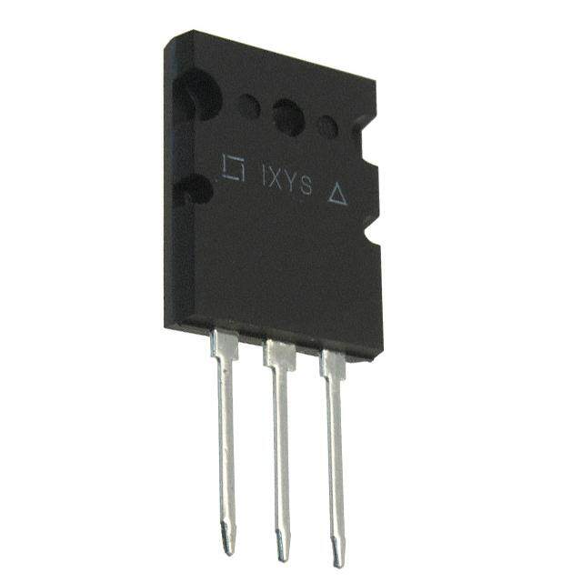
| 描述 | MOSFET P-CH 12V 750MA SOT-23MOSFET TAPE7 MOSFET |
| 产品分类 | FET - 单分离式半导体 |
| FET功能 | 逻辑电平门 |
| FET类型 | MOSFET P 通道,金属氧化物 |
| Id-ContinuousDrainCurrent | 750 mA |
| Id-连续漏极电流 | 750 mA |
| 品牌 | NXP Semiconductors |
| 产品手册 | |
| 产品图片 |
|
| rohs | 符合RoHS无铅 / 符合限制有害物质指令(RoHS)规范要求 |
| 产品系列 | 晶体管,MOSFET,NXP Semiconductors BSH205,215- |
| 数据手册 | |
| 产品型号 | BSH205,215 |
| PCN封装 | |
| PCN过时产品 | |
| Pd-PowerDissipation | 417 mW |
| Pd-功率耗散 | 417 mW |
| RdsOn-Drain-SourceResistance | 180 mOhms |
| RdsOn-漏源导通电阻 | 180 mOhms |
| Vds-Drain-SourceBreakdownVoltage | 12 V |
| Vds-漏源极击穿电压 | - 12 V |
| Vgs-Gate-SourceBreakdownVoltage | +/- 8 V |
| Vgs-栅源极击穿电压 | 8 V |
| 上升时间 | 4.5 ns |
| 下降时间 | 4.5 ns |
| 不同Id时的Vgs(th)(最大值) | 680mV @ 1mA |
| 不同Vds时的输入电容(Ciss) | 200pF @ 9.6V |
| 不同Vgs时的栅极电荷(Qg) | 3.8nC @ 4.5V |
| 不同 Id、Vgs时的 RdsOn(最大值) | 400 毫欧 @ 430mA,4.5V |
| 产品种类 | MOSFET |
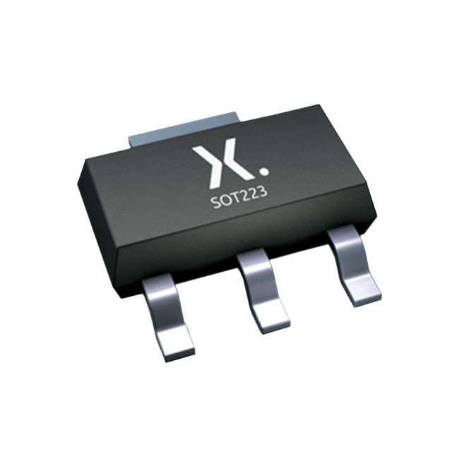
| 供应商器件封装 | SOT-23 (TO-236AB) |
| 其它名称 | 568-8028-1 |
| 典型关闭延迟时间 | 45 ns |
| 功率-最大值 | 417mW |
| 包装 | 剪切带 (CT) |
| 商标 | NXP Semiconductors |
| 安装类型 | 表面贴装 |
| 安装风格 | SMD/SMT |
| 封装 | Reel |
| 封装/外壳 | TO-236-3,SC-59,SOT-23-3 |
| 封装/箱体 | SOT-23-3 |
| 工厂包装数量 | 3000 |
| 晶体管极性 | P-Channel |
| 最大工作温度 | + 150 C |
| 最小工作温度 | - 55 C |
| 标准包装 | 1 |
| 漏源极电压(Vdss) | 12V |
| 电流-连续漏极(Id)(25°C时) | 750mA (Ta) |
| 通道模式 | Enhancement |
| 配置 | Single |
| 零件号别名 | BSH205 T/R |


- 商务部:美国ITC正式对集成电路等产品启动337调查
- 曝三星4nm工艺存在良率问题 高通将骁龙8 Gen1或转产台积电
- 太阳诱电将投资9.5亿元在常州建新厂生产MLCC 预计2023年完工
- 英特尔发布欧洲新工厂建设计划 深化IDM 2.0 战略
- 台积电先进制程称霸业界 有大客户加持明年业绩稳了
- 达到5530亿美元!SIA预计今年全球半导体销售额将创下新高
- 英特尔拟将自动驾驶子公司Mobileye上市 估值或超500亿美元
- 三星加码芯片和SET,合并消费电子和移动部门,撤换高东真等 CEO
- 三星电子宣布重大人事变动 还合并消费电子和移动部门
- 海关总署:前11个月进口集成电路产品价值2.52万亿元 增长14.8%


PDF Datasheet 数据手册内容提取
Important notice Dear Customer, On 7 February 2017 the former NXP Standard Product business became a new company with the tradename Nexperia. Nexperia is an industry leading supplier of Discrete, Logic and PowerMOS semiconductors with its focus on the automotive, industrial, computing, consumer and wearable application markets In data sheets and application notes which still contain NXP or Philips Semiconductors references, use the references to Nexperia, as shown below. Instead of http://www.nxp.com, http://www.philips.com/ or http://www.semiconductors.philips.com/, use http://www.nexperia.com Instead of sales.addresses@www.nxp.com or sales.addresses@www.semiconductors.philips.com, use salesaddresses@nexperia.com (email) Replace the copyright notice at the bottom of each page or elsewhere in the document, depending on the version, as shown below: - © NXP N.V. (year). All rights reserved or © Koninklijke Philips Electronics N.V. (year). All rights reserved Should be replaced with: - © Nexperia B.V. (year). All rights reserved. If you have any questions related to the data sheet, please contact our nearest sales office via e-mail or telephone (details via salesaddresses@nexperia.com). Thank you for your cooperation and understanding, Kind regards, Team Nexperia
Philips Semiconductors Product specification P-channel enhancement mode BSH205 MOS transistor FEATURES SYMBOL QUICK REFERENCE DATA • Very low threshold voltage s VDS = -12 V • Fast switching • Logic level compatible I = -0.75 A D • Subminiature surface mount g package R ≤ 0.5 Ω (V = -2.5 V) DS(ON) GS V ≥ 0.4 V GS(TO) d GENERAL DESCRIPTION PINNING SOT23 P-channel, enhancement mode, PIN DESCRIPTION logic level, field-effect power transistor. This device has low 1 gate 3 threshold voltage and extremely Top view fast switching making it ideal for 2 source battery powered applications and highspeeddigitalinterfacing. 3 drain The BSH205 is supplied in the 1 2 SOT23 subminiature surface mountingpackage. LIMITING VALUES Limiting values in accordance with the Absolute Maximum System (IEC 134) SYMBOL PARAMETER CONDITIONS MIN. MAX. UNIT V Drain-source voltage - -12 V DS V Drain-gate voltage R = 20 kΩ - -12 V DGR GS V Gate-source voltage - ± 8 V GS I Drain current (DC) T = 25 ˚C - -0.75 A D a T = 100 ˚C - -0.47 A a I Drain current (pulse peak value) T = 25 ˚C - -3 A DM a P Total power dissipation T = 25 ˚C - 0.417 W tot a T = 100 ˚C - 0.17 W a T , T Storage & operating temperature - 55 150 ˚C stg j THERMAL RESISTANCES SYMBOL PARAMETER CONDITIONS TYP. MAX. UNIT R Thermal resistance junction to FR4 board, minimum 300 - K/W th j-a ambient footprint August 1998 1 Rev 1.000
Philips Semiconductors Product specification P-channel enhancement mode BSH205 MOS transistor ELECTRICAL CHARACTERISTICS T= 25˚C unless otherwise specified j SYMBOL PARAMETER CONDITIONS MIN. TYP. MAX. UNIT V Drain-source breakdown V = 0 V; I = -10 μA -12 - - V (BR)DSS GS D voltage V Gate threshold voltage V = V ; I = -1 mA -0.4 -0.68 - V GS(TO) DS GS D T = 150˚C -0.1 - - V j R Drain-source on-state V = -4.5 V; I = -430 mA - 0.18 0.4 Ω DS(ON) GS D resistance V = -2.5 V; I = -430 mA - 0.32 0.5 Ω GS D V = -1.8 V; I = -210 mA - 0.42 0.6 Ω GS D V = -2.5 V; I = -430 mA; T = 150˚C - 0.48 0.75 Ω GS D j g Forward transconductance V = -9.6 V; I = -430 mA 0.5 1.6 - S fs DS D I Gate source leakage current V = ±8 V; V = 0 V - ±10 ±100 nA GSS GS DS I Zero gate voltage drain V = -9.6 V; V = 0 V; - -50 -100 nA DSS DS GS current T = 150˚C - -11 -100 μA j Q Total gate charge I = -0.5 A; V = -10 V; V = -4.5 V - 3.8 - nC g(tot) D DD GS Q Gate-source charge - 0.4 - nC gs Q Gate-drain (Miller) charge - 1.0 - nC gd t Turn-on delay time V = -10 V; I = -0.5 A; - 2 - ns d on DD D t Turn-on rise time V = -8 V; R = 6 Ω - 4.5 - ns r GS G t Turn-off delay time Resistive load - 45 - ns d off t Turn-off fall time - 20 - ns f C Input capacitance V = 0 V; V = -9.6 V; f = 1 MHz - 200 - pF iss GS DS C Output capacitance - 95 - pF oss C Feedback capacitance - 41 - pF rss REVERSE DIODE LIMITING VALUES AND CHARACTERISTICS T = 25˚C unless otherwise specified j SYMBOL PARAMETER CONDITIONS MIN. TYP. MAX. UNIT I Continuous reverse drain T = 25 ˚C - - -0.75 A DR a current I Pulsed reverse drain current - - -3 A DRM V Diode forward voltage I = -0.38 A; V = 0 V - -0.72 -1.3 V SD F GS t Reverse recovery time I = -0.5 A; -dI /dt = 100 A/μs; - 75 - ns rr F F Q Reverse recovery charge V = 0 V; V = -9.6 V - 69 - nC rr GS R August 1998 2 Rev 1.000
Philips Semiconductors Product specification P-channel enhancement mode BSH205 MOS transistor Normalised Power Dissipation, PD (%) Peak Pulsed Drain Current, IDM (A) BSH105 120 1000 100 D = 0.5 100 80 0.2 0.1 0.05 60 10 0.02 P D = tp/T D tp 40 single pulse 1 20 T 0 0.1 0 25 50 75 100 125 150 1E-06 1E-05 1E-04 1E-03 1E-02 1E-01 1E+00 1E+01 Ambient Temperature, Ta (C) Pulse width, tp (s) Fig.1. Normalised power dissipation. Fig.4. Transient thermal impedance. PD% = 100⋅P/P = f(T) Z = f(t); parameter D = t/T D D 25 ˚C a th j-a p Normalised Drain Current, ID (%) Drain current, ID (A) BSH205 120 -1.4 4.5 V -2.5 V -1.8 V Tj = 25 C 100 -1.2 VGS = -1.4 V -1 80 -1.3 V -0.8 60 -1.2 V -0.6 40 -1.1 V -0.4 20 -1 V -0.2 -0.9 V 0 0 25 50 75 100 125 150 0 0 -0.5 -1 -1.5 -2 Ambient Temperature, Ta (C) Drain-Source Voltage, VDS (V) Fig.2. Normalised continuous drain current. Fig.5. Typical output characteristics, T = 25 ˚C. ID% = 100⋅I/I = f(T); conditions: V ≤ -10 V I = f(V ); parameter V j D D 25 ˚C a GS D DS GS Drain-Source On Resistance, RDS(on) (Ohms) BSH205 100 Peak Pulsed Drain Current, IDM (A) BSH205 2.83 -0.9 V -1V -1.2 V Tj = 25 C 2.6 -1.1 V -1.3 V 2.4 2.2 10 RDS(on) = VDS/ ID tp = 100 us 2 -1.4 V 1.8 1 ms 1.6 1 10 ms 1.4 1.2 100 ms 1 0.1 d.c. 00..68 -2.5 V -1.8 V 0.4 0.2 VGS = -4.5V 0.01 0 0.1 1 10 100 0 -0.2 -0.4 -0.6 -0.8 -1 -1.2 -1.4 Drain-Source Voltage, VDS (V) Drain Current, ID (A) Fig.3. Safe operating area. T = 25 ˚C Fig.6. Typical on-state resistance, T = 25 ˚C. a j I & I = f(V ); I single pulse; parameter t R = f(I); parameter V D DM DS DM p DS(ON) D GS August 1998 3 Rev 1.000
Philips Semiconductors Product specification P-channel enhancement mode BSH205 MOS transistor Drain Current, ID (A) BSH205 -3 Threshold Voltage, VGS(to), (V) 0.7 VDS > ID X RDS(on) -2.5 Tj = 25 C 0.6 150 C -2 0.5 typical 0.4 -1.5 minimum 0.3 -1 0.2 -0.5 0.1 0 0 0 25 50 75 100 125 150 0 -0.5 -1 -1.5 -2 -2.5 -3 Gate-Source Voltage, VGS (V) Junction Temperature, Tj (C) Fig.7. Typical transfer characteristics. Fig.10. Gate threshold voltage. I = f(V ) V = f(T); conditions: I = 1 mA; V = V D GS GS(TO) j D DS GS Transconductance, gfs (S) BSH205 Drain Current, ID (A) BSH205 3.5 1E-01 VDS > ID X RDS(on) VDS = -5 V 3 Tj = 25 C 1E-02 Tj = 25 C 2.5 150 C 1E-03 2 1E-04 1.5 1 1E-05 0.5 1E-06 0 0 -0.2 -0.4 -0.6 -0.8 -1 -1.2 -1.4 -1.6 -1.8 -2 -2.2 -2.4 -2.6 1E-07 -1 -0.9 -0.8 -0.7 -0.6 -0.5 -0.4 -0.3 -0.2 -0.1 0 Drain Current, ID (A) Gate-Source Voltage, VGS (V) Fig.8. Typical transconductance, T = 25 ˚C. Fig.11. Sub-threshold drain current. j g = f(I) I = f(V ; conditions: T = 25 ˚C fs D D GS) j Normalised Drain-Source On Resistance Capacitances, Ciss, Coss, Crss (pF) BSH205 2 1000 1.9 RDS(ON) @ Tj 1.8 1.7 RDS(ON) @ 25C -2.5 V 1.6 1.5 VGS = -4.5 V Ciss 1.4 1.3 -1.8 V 1.2 100 Coss 1.1 1 0.9 Crss 0.8 0.7 0.6 0.5 10 0 25 50 75 100 125 150 -0.1 -1.0 -10.0 -100.0 Junction Temperature, Tj (C) Drain-Source Voltage, VDS (V) Fig.9. Normalised drain-source on-state resistance. Fig.12. Typical capacitances, C , C , C . iss oss rss R /R = f(T) C = f(V ); conditions: V = 0 V; f = 1 MHz DS(ON) DS(ON)25 ˚C j DS GS August 1998 4 Rev 1.000
Philips Semiconductors Product specification P-channel enhancement mode BSH205 MOS transistor Gate-source voltage, VGS (V) BSH205 Source-Drain Diode Current, IF (A) BSH205 -6 5 VDD = 10 V 4.5 -5 RD = 20 Ohms 4 Tj = 25 C 3.5 -4 3 -3 2.5 2 150 C Tj = 25 C -2 1.5 1 -1 0.5 0 0 0 0.2 0.4 0.6 0.8 1 1.2 1.4 0 1 2 3 4 5 Gate charge, (nC) Drain-Source Voltage, VSDS (V) Fig.13. Typical turn-on gate-charge characteristics. Fig.14. Typical reverse diode current. V = f(Q) I = f(V ); conditions: V = 0 V; parameter T GS G F SDS GS j August 1998 5 Rev 1.000
Philips Semiconductors Product specification P-channel enhancement mode BSH205 MOS transistor MECHANICAL DATA Plastic surface mounted package; 3 leads SOT23 D B E A X HE vM A 3 Q A A1 1 2 c e1 bp wM B Lp e detail X 0 1 2 mm scale DIMENSIONS (mm are the original dimensions) UNIT A mAa1x. bp c D E e e1 HE Lp Q v w mm 10..19 0.1 00..4388 00..1059 32..08 11..42 1.9 0.95 22..51 00..4155 00..5455 0.2 0.1 VOEURTSLIIONEN IEC JEDEC REFERENCES EIAJ PERUORJOEPCETAIONN ISSUE DATE SOT23 97-02-28 Fig.15. SOT23 surface mounting package. Notes 1. This product is supplied in anti-static packaging. The gate-source input must be protected against static discharge during transport or handling. 2. Refer to SMD Footprint Design and Soldering Guidelines, Data Handbook SC18. 3. Epoxy meets UL94 V0 at 1/8". August 1998 6 Rev 1.000