ICGOO在线商城 > 分立半导体产品 > 晶体管 - FET,MOSFET - 单 > SUD50N06-09L-E3
 Datasheet下载
- 型号: SUD50N06-09L-E3
- 制造商: Vishay
- 库位|库存: xxxx|xxxx
- 要求:
| 数量阶梯 | 香港交货 | 国内含税 |
| +xxxx | $xxxx | ¥xxxx |
查看当月历史价格
查看今年历史价格
SUD50N06-09L-E3产品简介:
ICGOO电子元器件商城为您提供SUD50N06-09L-E3由Vishay设计生产,在icgoo商城现货销售,并且可以通过原厂、代理商等渠道进行代购。 SUD50N06-09L-E3价格参考。VishaySUD50N06-09L-E3封装/规格:晶体管 - FET,MOSFET - 单, 表面贴装 N 沟道 60V 50A(Tc) 3W(Ta),136W(Tc) TO-252,(D-Pak)。您可以下载SUD50N06-09L-E3参考资料、Datasheet数据手册功能说明书,资料中有SUD50N06-09L-E3 详细功能的应用电路图电压和使用方法及教程。
Vishay Siliconix的SUD50N06-09L-E3是一款单通道MOSFET(金属氧化物场效应晶体管),具体型号为SUD50N06-09L-E3。它具有低导通电阻和高开关速度,适用于多种应用场景,特别是在需要高效能和低功耗的电路中。

 应用场景:

1. 电源管理:
   - DC-DC转换器:该MOSFET可用于降压、升压或升降压DC-DC转换器中,作为主开关或同步整流器,提高转换效率,减少功率损耗。
   - 线性稳压器:在低压差线性稳压器(LDO)中,SUD50N06-09L-E3可以用于旁路开关,以实现高效的电源切换。

2. 电机驱动:
   - 无刷直流电机(BLDC):在电机驱动应用中,该MOSFET可以用于H桥或三相逆变器电路,控制电机的速度和方向,确保高效运行。
   - 步进电机:用于步进电机驱动器中的电流控制和方向切换,提供精确的控制和较低的发热。

3. 电池管理系统(BMS):
   - 电池保护电路:SUD50N06-09L-E3可用于电池组的充放电保护电路中,防止过充、过放、短路等异常情况,确保电池的安全性和寿命。
   - 电池均衡:在电池均衡电路中,MOSFET可以用于调节不同电池单元之间的电压差异,保持电池组的一致性。

4. 负载开关:
   - 便携式设备:在智能手机、平板电脑、笔记本电脑等便携式设备中,该MOSFET可以用作负载开关,快速切断或接通电源,延长电池续航时间。
   - 工业控制系统:用于工业自动化设备中的负载控制,确保系统的稳定性和可靠性。

5. 汽车电子:
   - 车载充电器:在车载充电器中,SUD50N06-09L-E3可以用于功率转换和保护电路,确保充电过程的安全性和效率。
   - 电动助力转向系统(EPS):用于电动助力转向系统的电源管理和电机驱动,提供快速响应和高可靠性。

总之,SUD50N06-09L-E3凭借其优异的电气性能和可靠性,广泛应用于各种电力电子设备中,尤其是在需要高效能和低功耗的应用场景中表现出色。
| 参数 | 数值 |
| 产品目录 | |
| ChannelMode | Enhancement |
| 描述 | MOSFET N-CH 60V 50A TO252MOSFET 60V 50A 136W 9.3mohm @ 10V |
| 产品分类 | FET - 单分离式半导体 |
| FET功能 | 逻辑电平门 |
| FET类型 | MOSFET N 通道,金属氧化物 |
| Id-ContinuousDrainCurrent | 50 A |
| Id-连续漏极电流 | 50 A |
| 品牌 | Vishay / SiliconixVishay Siliconix |
| 产品手册 | http://www.vishay.com/doc?72004 |
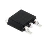
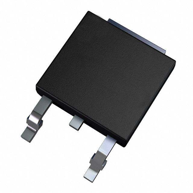
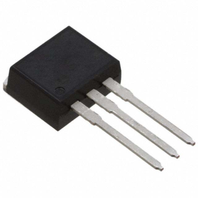
| 产品图片 |
|
| rohs | RoHS 合规性豁免无铅 / 符合限制有害物质指令(RoHS)规范要求 |
| 产品系列 | 晶体管,MOSFET,Vishay / Siliconix SUD50N06-09L-E3TrenchFET® |
| 数据手册 | |
| 产品型号 | SUD50N06-09L-E3SUD50N06-09L-E3 |
| Pd-PowerDissipation | 136 W |
| Pd-功率耗散 | 136 W |
| RdsOn-Drain-SourceResistance | 9 mOhms |
| RdsOn-漏源导通电阻 | 9 mOhms |
| Vds-Drain-SourceBreakdownVoltage | 60 V |
| Vds-漏源极击穿电压 | 60 V |
| Vgs-Gate-SourceBreakdownVoltage | +/- 20 V |
| Vgs-栅源极击穿电压 | 20 V |
| 上升时间 | 15 ns |
| 下降时间 | 20 ns |
| 不同Id时的Vgs(th)(最大值) | 3V @ 250µA |
| 不同Vds时的输入电容(Ciss) | 2650pF @ 25V |
| 不同Vgs时的栅极电荷(Qg) | 70nC @ 10V |
| 不同 Id、Vgs时的 RdsOn(最大值) | 9.3 毫欧 @ 20A,10V |
| 产品种类 | MOSFET |
| 供应商器件封装 | TO-252,(D-Pak) |
| 其它名称 | SUD50N06-09L-E3DKR |
| 典型关闭延迟时间 | 35 ns |
| 功率-最大值 | 136W |
| 包装 | Digi-Reel® |
| 商标 | Vishay / Siliconix |
| 安装类型 | 表面贴装 |
| 安装风格 | SMD/SMT |
| 封装 | Reel |
| 封装/外壳 | TO-252-3,DPak(2 引线+接片),SC-63 |
| 封装/箱体 | DPAK-2 |
| 工厂包装数量 | 2000 |
| 晶体管极性 | N-Channel |
| 最大工作温度 | + 175 C |
| 最小工作温度 | - 55 C |
| 标准包装 | 1 |
| 漏源极电压(Vdss) | 60V |
| 电流-连续漏极(Id)(25°C时) | 50A (Tc) |
| 通道模式 | Enhancement |
| 配置 | Single |


PDF Datasheet 数据手册内容提取
SUD50N06-09L Vishay Siliconix N-Channel 60 V (D-S), 175 °C MOSFET, Logic Level FEATURES PRODUCT SUMMARY • 175 °C Junction Temperature VDS (V) RDS(on) () ID (A)a (cid:129) TrenchFET® Power MOSFET 0.0093 at VGS = 10 V 50 (cid:129) Material categorization: 60 0.0122 at VGS = 4.5 V 50 For definitions of compliance please see www.vishay.com/doc?99912 TO-252 D G Drain Connected to Tab G D S S Top View Ordering Information: N-Channel MOSFET SUD50N06-09L-E3 (Lead (Pb)-free) ABSOLUTE MAXIMUM RATINGS (T = 25°C, unless otherwise noted) C Parameter Symbol Limit Unit Gate-Source Voltage VGS ± 20 V Continuous Drain Current (TJ = 175 °C)b TTCC == 12050 ° °CC ID 5500a Pulsed Drain Current IDM 100 A Continuous Source Current (Diode Conduction) IS 50a Avalanche Current IAS 50 Single Avalanche Energy (Duty Cycle 1 %) L = 0.1 mH EAS 125 mJ TC = 25 °C 136 Maximum Power Dissipation PD W TA = 25 °C 3b, 8.3b, c Operating Junction and Storage Temperature Range TJ, Tstg - 55 to 175 °C THERMAL RESISTANCE RATINGS Parameter Symbol Typical Maximum Unit t 10 sec 15 18 Maximum Junction-to-Ambienta Steady State RthJA 40 50 °C/W Maximum Junction-to-Case RthJC 0.85 1.1 Notes: a. Package limited. b. Surface mounted on 1" x 1" FR4 board. c. t 10 s. Document Number: 72004 For technical questions, contact: pmostechsupport@vishay.com www.vishay.com S13-0298-Rev. F, 11-Feb-13 1 This document is subject to change without notice. THE PRODUCTS DESCRIBED HEREIN AND THIS DOCUMENT ARE SUBJECT TO SPECIFIC DISCLAIMERS, SET FORTH AT www.vishay.com/doc?91000
SUD50N06-09L Vishay Siliconix SPECIFICATIONS (T = 25°C, unless otherwise noted) J Parameter Symbol Test Conditions Min. Typ.a Max. Unit Static Drain-Source Breakdown Voltage VDS VGS = 0 V, ID = 250 µA 60 V Gate Threshold Voltage VGS(th) VDS = VGS, ID = 250 µA 1 2 3 Gate-Body Leakage IGSS VDS = 0 V, VGS = ± 20 V ± 100 nA VDS = 60 V, VGS = 0 V 1 Zero Gate Voltage Drain Current IDSS VDS = 60 V, VGS = 0 V, TJ = 125 °C 50 µA VDS = 60 V, VGS = 0 V, TJ = 175 °C 250 On-State Drain Currentb ID(on) VDS =5 V, VGS = 10 V 50 A VGS = 10 V, ID = 20 A 0.0074 0.0093 VGS = 10 V, ID = 20 A, TJ = 125 °C 0.0160 Drain-Source On-State Resistanceb RDS(on) VGS = 10 V, ID = 20 A, TJ = 175 °C 0.0200 VGS = 4.5 V, ID = 15 A 0.0122 Forward Transconductanceb gfs VDS = 15 V, ID = 20 A 60 S Dynamic Input Capacitance Ciss 2650 Output Capacitance Coss VGS = 0 V, VDS = 25 V, f = 1 MHz 470 pF Reverse Transfer Capacitance Crss 225 Total Gate Chargec Qg 47 70 Gate-Source Chargec Qgs VDS = 30 V, VGS = 10 V, ID = 50 A 10 nC Gate-Drain Chargec Qgd 12 Turn-On Delay Timec td(on) 10 20 Rise Timec tr VDD = 30 V, RL = 0.6 15 25 ns Turn-Off Delay Timec td(off) ID 50 A, VGEN = 10 V, Rg = 2.5 35 50 Fall Timec tf 20 30 Source-Drain Diode Ratings and Characteristics (T = 25°C) C Pulsed Current ISM 100 A Diode Forward Voltage VSD IF = 20 A, VGS = 0 V 1 1.5 V Reverse Recovery Time trr IF = 20 A, di/dt = 100 A/µs 45 100 ns Notes: a. For design aid only; not subject to production testing. b. Pulse test; pulse width 300 µs, duty cycle 2 %. c. Independent of operating temperature. Stresses beyond those listed under “Absolute Maximum Ratings” may cause permanent damage to the device. These are stress ratings only, and functional operation of the device at these or any other conditions beyond those indicated in the operational sections of the specifications is not implied. Exposure to absolute maximum rating conditions for extended periods may affect device reliability. Document Number: 72004 For technical questions, contact: pmostechsupport@vishay.com www.vishay.com S13-0298-Rev. F, 11-Feb-13 2 This document is subject to change without notice. THE PRODUCTS DESCRIBED HEREIN AND THIS DOCUMENT ARE SUBJECT TO SPECIFIC DISCLAIMERS, SET FORTH AT www.vishay.com/doc?91000
SUD50N06-09L Vishay Siliconix TYPICAL CHARACTERISTICS (25°C unless noted) 100 100 VGS = 10 thru 5 V 80 80 Current (A) 60 4 V Current (A) 60 Drain 40 Drain 40 - D - D I I TC = 125 °C 20 20 25 °C 2 V, 3 V -55 °C 0 0 0 2 4 6 8 10 0 1 2 3 4 5 VDS - Drain-to-Source Voltage (V) VGS - Gate-to-Source Voltage (V) Output Characteristics Transfer Characteristics 120 0.015 TC = -55 °C 100 0.012 e (S) 25 °C VGS = 4.5 V c 80 n cta 0.009 VGS = 10 V du 125 °C n 60 o c s n 0.006 a - - Tr 40 S(on) gfs RD0.003 20 0 0.000 0 10 20 30 40 50 0 20 40 60 80 100 ID - Drain Current (A) ID - Drain Current (A) Transconductance On-Resistance vs. Drain Current 4000 10 3500 3000 ge (V) 8 IVDD =S 5=0 3 A0 V pF) Ciss olta ance (2500 urce V 6 cit2000 So pa o- Ca1500 e-t 4 C - Gat 1000 - S Coss VG 2 500 Crss 0 0 0 10 20 30 40 50 60 0 10 20 30 40 50 VDS - Drain-to-Source Voltage (V) Qg - Total Gate Charge (nC) Capacitance Gate Charge Document Number: 72004 For technical questions, contact: pmostechsupport@vishay.com www.vishay.com S13-0298-Rev. F, 11-Feb-13 3 This document is subject to change without notice. THE PRODUCTS DESCRIBED HEREIN AND THIS DOCUMENT ARE SUBJECT TO SPECIFIC DISCLAIMERS, SET FORTH AT www.vishay.com/doc?91000
SUD50N06-09L Vishay Siliconix TYPICAL CHARACTERISTICS (25°C unless noted) 2.5 100 VGS = 10 V ed) ID = 20 A aliz 2.0 stance(Norm 1.5 e Current (A) 10 TJ = 150 °C TJ = 25 °C Resi 1.0 ourc On- - S - n) IS S(o 0.5 D R 0.0 1 -50 -25 0 25 50 75 100 125 150 175 0 0.3 0.6 0.9 1.2 1.5 TJ - Junction Temperature (°C) VSD - Source-to-Drain Voltage (V) On-Resistance vs. Junction Temperature Source-Drain Diode Forward Voltage Document Number: 72004 For technical questions, contact: pmostechsupport@vishay.com www.vishay.com S13-0298-Rev. F, 11-Feb-13 4 This document is subject to change without notice. THE PRODUCTS DESCRIBED HEREIN AND THIS DOCUMENT ARE SUBJECT TO SPECIFIC DISCLAIMERS, SET FORTH AT www.vishay.com/doc?91000
SUD50N06-09L Vishay Siliconix THERMAL RATINGS 60 1000 Limited by RDS(on)* 50 100 10 µs 100 µs A) 40 A) nt ( nt ( 10 e e urr urr 1 ms n C 30 n C 10 ms Drai Drai 1 D10C0 ms - D 20 - D I I 0.1 TC = 25 °C 10 Single Pulse 0 0.01 0 25 50 75 100 125 150 175 0.1 1 10 100 TA - Ambient Temperature (°C) VDS - Drain-to-Source Voltage (V) * VGS > minimum VGS at which RDS(on) is specified Maximum Drain Current vs. Ambient Temperature Safe Operating Area 2 1 Duty Cycle = 0.5 nt e e Transiedance 00.2.1 ed Effectivermal Imp 0.1 0.05 zh aliT 0.02 m Nor Single Pulse 0.01 10-4 10-3 10-2 10-1 1 10 100 Square Wave Pulse Duration (s) Normalized Thermal Transient Impedance, Junction-to-Case Vishay Siliconix maintains worldwide manufacturing capability. Products may be manufactured at one of several qualified locations. Reliability data for Silicon Technology and Package Reliability represent a composite of all qualified locations. For related documents such as package/tape drawings, part marking, and reliability data, see www.vishay.com/ppg?72004. Document Number: 72004 For technical questions, contact: pmostechsupport@vishay.com www.vishay.com S13-0298-Rev. F, 11-Feb-13 5 This document is subject to change without notice. THE PRODUCTS DESCRIBED HEREIN AND THIS DOCUMENT ARE SUBJECT TO SPECIFIC DISCLAIMERS, SET FORTH AT www.vishay.com/doc?91000
Package Information www.vishay.com Vishay Siliconix TO-252AA Case Outline E A MILLIMETERS INCHES C2 b3 DIM. MIN. MAX. MIN. MAX. 3 A 2.18 2.38 0.086 0.094 L A1 - 0.127 - 0.005 b 0.64 0.88 0.025 0.035 b2 0.76 1.14 0.030 0.045 D b3 4.95 5.46 0.195 0.215 H C 0.46 0.61 0.018 0.024 C2 0.46 0.89 0.018 0.035 L4 5 D 5.97 6.22 0.235 0.245 L L m) D1 4.10 - 0.161 - m 5 E 6.35 6.73 0.250 0.265 0. b b2 ght ( C E1 4.32 - 0.170 - e ei H 9.40 10.41 0.370 0.410 h A1 e1 ne e 2.28 BSC 0.090 BSC a pl e1 4.56 BSC 0.180 BSC e g a L 1.40 1.78 0.055 0.070 g L3 0.89 1.27 0.035 0.050 1 D L4 - 1.02 - 0.040 L5 1.01 1.52 0.040 0.060 ECN: T16-0236-Rev. P, 16-May-16 DWG: 5347 E1 Notes • Dimension L3 is for reference only. Revision: 16-May-16 1 Document Number: 71197 For technical questions, contact: pmostechsupport@vishay.com THIS DOCUMENT IS SUBJECT TO CHANGE WITHOUT NOTICE. THE PRODUCTS DESCRIBED HEREIN AND THIS DOCUMENT ARE SUBJECT TO SPECIFIC DISCLAIMERS, SET FORTH AT www.vishay.com/doc?91000
Application Note 826 Vishay Siliconix RECOMMENDED MINIMUM PADS FOR DPAK (TO-252) 0.224 (5.690) 3 0) 4 8 2 1 0. 6. ( 0.420 10.668) ( 7 2) 8 0 0 2 0. 2. ( 0 6) 9 8 0 2 0. 2. ( 0.180 0.055 (4.572) (1.397) Recommended Minimum Pads Dimensions in Inches/(mm) Return to Index Return to Index A P P L I C A T I O N N O T E Document Number: 72594 www.vishay.com Revision: 21-Jan-08 3
Legal Disclaimer Notice www.vishay.com Vishay Disclaimer ALL PRODUCT, PRODUCT SPECIFICATIONS AND DATA ARE SUBJECT TO CHANGE WITHOUT NOTICE TO IMPROVE RELIABILITY, FUNCTION OR DESIGN OR OTHERWISE. Vishay Intertechnology, Inc., its affiliates, agents, and employees, and all persons acting on its or their behalf (collectively, “Vishay”), disclaim any and all liability for any errors, inaccuracies or incompleteness contained in any datasheet or in any other disclosure relating to any product. Vishay makes no warranty, representation or guarantee regarding the suitability of the products for any particular purpose or the continuing production of any product. To the maximum extent permitted by applicable law, Vishay disclaims (i) any and all liability arising out of the application or use of any product, (ii) any and all liability, including without limitation special, consequential or incidental damages, and (iii) any and all implied warranties, including warranties of fitness for particular purpose, non-infringement and merchantability. Statements regarding the suitability of products for certain types of applications are based on Vishay’s knowledge of typical requirements that are often placed on Vishay products in generic applications. Such statements are not binding statements about the suitability of products for a particular application. It is the customer’s responsibility to validate that a particular product with the properties described in the product specification is suitable for use in a particular application. Parameters provided in datasheets and / or specifications may vary in different applications and performance may vary over time. All operating parameters, including typical parameters, must be validated for each customer application by the customer’s technical experts. Product specifications do not expand or otherwise modify Vishay’s terms and conditions of purchase, including but not limited to the warranty expressed therein. Except as expressly indicated in writing, Vishay products are not designed for use in medical, life-saving, or life-sustaining applications or for any other application in which the failure of the Vishay product could result in personal injury or death. Customers using or selling Vishay products not expressly indicated for use in such applications do so at their own risk. Please contact authorized Vishay personnel to obtain written terms and conditions regarding products designed for such applications. No license, express or implied, by estoppel or otherwise, to any intellectual property rights is granted by this document or by any conduct of Vishay. Product names and markings noted herein may be trademarks of their respective owners. © 2017 VISHAY INTERTECHNOLOGY, INC. ALL RIGHTS RESERVED Revision: 08-Feb-17 1 Document Number: 91000
Mouser Electronics Authorized Distributor Click to View Pricing, Inventory, Delivery & Lifecycle Information: V ishay: SUD50N06-09L SUD50N06-09L-E3