ICGOO在线商城 > 分立半导体产品 > 晶体管 - FET,MOSFET - 单 > STD3NK80ZT4
 Datasheet下载
- 型号: STD3NK80ZT4
- 制造商: STMicroelectronics
- 库位|库存: xxxx|xxxx
- 要求:
| 数量阶梯 | 香港交货 | 国内含税 |
| +xxxx | $xxxx | ¥xxxx |
查看当月历史价格
查看今年历史价格
STD3NK80ZT4产品简介:
ICGOO电子元器件商城为您提供STD3NK80ZT4由STMicroelectronics设计生产,在icgoo商城现货销售,并且可以通过原厂、代理商等渠道进行代购。 STD3NK80ZT4价格参考¥1.98-¥2.48。STMicroelectronicsSTD3NK80ZT4封装/规格:晶体管 - FET,MOSFET - 单, N-Channel 800V 2.5A (Tc) 70W (Tc) Surface Mount DPAK。您可以下载STD3NK80ZT4参考资料、Datasheet数据手册功能说明书,资料中有STD3NK80ZT4 详细功能的应用电路图电压和使用方法及教程。
STMicroelectronics 的 STD3NK80ZT4 是一款高压 N 沟道增强型功率 MOSFET,属于晶体管 - FET 分类中的单MOSFET产品。该器件耐压高达 800V,适用于高电压、低电流的开关电源应用。

其主要应用场景包括:
1. 开关电源(SMPS):广泛用于反激式、正激式等拓扑结构的AC-DC转换器中,如手机充电器、适配器、电视机和显示器电源模块。
2. 照明电源:适用于LED 驱动电源、电子镇流器等照明系统,具备良好的能效和稳定性。
3. 待机电源电路:在家电、工业控制设备中作为待机电源的主开关元件,实现低功耗运行。
4. 高电压 DC-DC 转换:用于需要高压输入的直流变换系统,如工业电源模块。

STD3NK80ZT4 采用先进的“超级结”(Super Junction)技术,具有较低的导通电阻(RDS(on))、优异的开关性能和高温可靠性,同时支持 TO-220FP 或类似封装,便于散热与安装。此外,其内置快速恢复体二极管,有助于减少外部元件数量,提升系统集成度与可靠性。

综上,该MOSFET特别适合对效率、空间和成本敏感的中低功率高压应用场合,是消费电子和工业电源设计中的常用选择。
| 参数 | 数值 |
| 产品目录 | |
| ChannelMode | Enhancement |
| 描述 | MOSFET N-CH 800V 2.5A DPAKMOSFET N-Ch 800 Volt 2.5A Zener SuperMESH |
| 产品分类 | FET - 单分离式半导体 |
| FET功能 | 标准 |
| FET类型 | MOSFET N 通道,金属氧化物 |
| Id-ContinuousDrainCurrent | 2.5 A |
| Id-连续漏极电流 | 2.5 A |
| 品牌 | STMicroelectronics |
| 产品手册 | |
| 产品图片 |
|
| rohs | 符合RoHS无铅 / 符合限制有害物质指令(RoHS)规范要求 |
| 产品系列 | 晶体管,MOSFET,STMicroelectronics STD3NK80ZT4SuperMESH™ |
| 数据手册 | |
| 产品型号 | STD3NK80ZT4 |
| Pd-PowerDissipation | 70 W |
| Pd-功率耗散 | 70 W |
| Qg-GateCharge | 19 nC |
| Qg-栅极电荷 | 19 nC |
| RdsOn-Drain-SourceResistance | 4.5 Ohms |
| RdsOn-漏源导通电阻 | 4.5 Ohms |
| Vds-Drain-SourceBreakdownVoltage | 800 V |
| Vds-漏源极击穿电压 | 800 V |
| Vgs-Gate-SourceBreakdownVoltage | +/- 30 V |
| Vgs-栅源极击穿电压 | 30 V |
| 上升时间 | 27 ns |
| 下降时间 | 40 ns |
| 不同Id时的Vgs(th)(最大值) | 4.5V @ 50µA |
| 不同Vds时的输入电容(Ciss) | 485pF @ 25V |
| 不同Vgs时的栅极电荷(Qg) | 19nC @ 10V |
| 不同 Id、Vgs时的 RdsOn(最大值) | 4.5 欧姆 @ 1.25A,10V |
| 产品目录页面 | |
| 产品种类 | MOSFET |
| 供应商器件封装 | D-Pak |
| 其它名称 | 497-7968-6 |
| 其它有关文件 | http://www.st.com/web/catalog/sense_power/FM100/CL824/SC1168/PF67227?referrer=70071840 |
| 典型关闭延迟时间 | 36 ns |
| 功率-最大值 | 70W |
| 包装 | Digi-Reel® |
| 商标 | STMicroelectronics |
| 安装类型 | 表面贴装 |
| 安装风格 | SMD/SMT |
| 封装 | Reel |
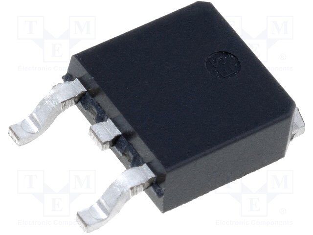
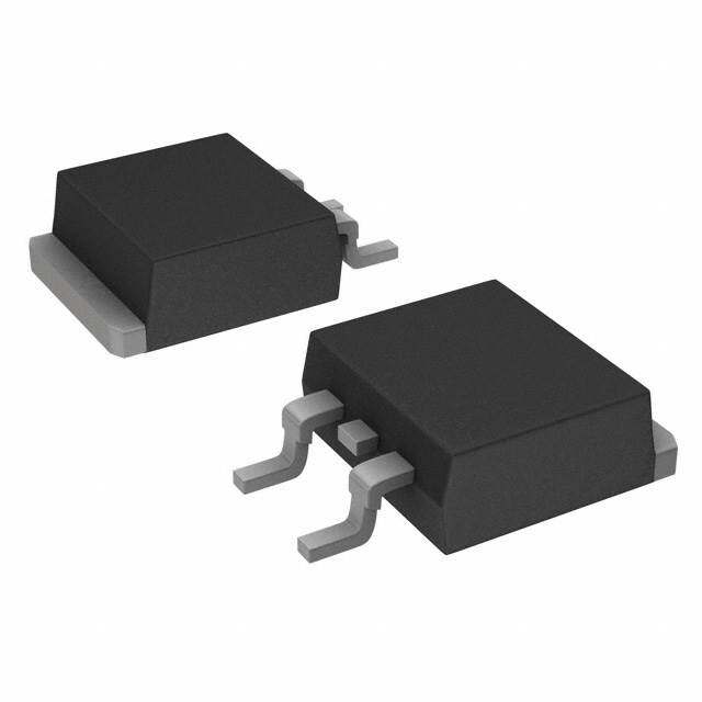
| 封装/外壳 | TO-252-3,DPak(2 引线+接片),SC-63 |
| 封装/箱体 | DPAK-2 |
| 工厂包装数量 | 2500 |
| 晶体管极性 | N-Channel |
| 最大工作温度 | + 150 C |
| 最小工作温度 | - 55 C |
| 标准包装 | 1 |
| 正向跨导-最小值 | 2.1 S |
| 漏源极电压(Vdss) | 800V |
| 电流-连续漏极(Id)(25°C时) | 2.5A (Tc) |
| 系列 | STD3NK80Z |
| 通道模式 | Enhancement |
| 配置 | Single |


- 商务部:美国ITC正式对集成电路等产品启动337调查
- 曝三星4nm工艺存在良率问题 高通将骁龙8 Gen1或转产台积电
- 太阳诱电将投资9.5亿元在常州建新厂生产MLCC 预计2023年完工
- 英特尔发布欧洲新工厂建设计划 深化IDM 2.0 战略
- 台积电先进制程称霸业界 有大客户加持明年业绩稳了
- 达到5530亿美元!SIA预计今年全球半导体销售额将创下新高
- 英特尔拟将自动驾驶子公司Mobileye上市 估值或超500亿美元
- 三星加码芯片和SET,合并消费电子和移动部门,撤换高东真等 CEO
- 三星电子宣布重大人事变动 还合并消费电子和移动部门
- 海关总署:前11个月进口集成电路产品价值2.52万亿元 增长14.8%


PDF Datasheet 数据手册内容提取
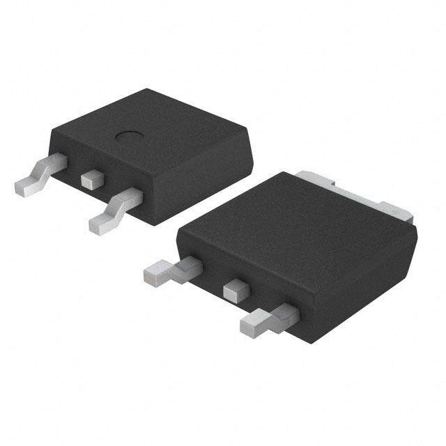
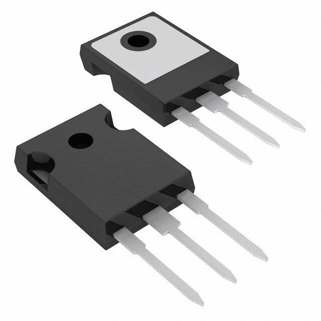
STD3NK80Z-1, STD3NK80ZT4, STF3NK80Z, STP3NK80Z N-channel 800 V, 3.8 Ω typ., 2.5 A SuperMESH™ Power MOSFETs in IPAK, DPAK, TO-220FP, TO-220 packages Datasheet - production data Features Order code VDS RDS(on) max. ID STD3NK80Z-1 800 V 4.5 Ω 2.5 A STD3NK80ZT4 800 V 4.5 Ω 2.5 A STF3NK80Z 800 V 4.5 Ω 2.5 A STP3NK80Z 800 V 4.5 Ω 2.5 A Extremely high dv/dt capability 100% avalanche tested Gate charge minimized Zener-protected Applications Figure 1: Internal schematic diagram Switching applications Description These high voltage devices are Zener-protected N-channel Power MOSFETs developed using the SuperMESH™ technology by STMicroelectronics, an optimization of the well-established PowerMESH™. In addition to a significant reduction in on-resistance, these devices are designed to ensure a high level of dv/dt capability for the most demanding applications. Such series complements ST's full range of high voltage MOSFETs including the revolutionary MDmesh™ products. Table 1: Device summary Order code Marking Package Packaging STD3NK80Z-1 D3NK80Z IPAK Tube STD3NK80ZT4 D3NK80Z DPAK Tape and reel STF3NK80Z F3NK80Z TO-220FP Tube STP3NK80Z P3NK80Z TO-220 Tube April 2017 DocID9565 Rev 7 1/29 This is information on a product in full production. www.st.com
Contents STD3NK80Z-1, STD3NK80ZT4, STF3NK80Z, STP3NK80Z Contents 1 Electrical ratings ............................................................................. 3 2 Electrical characteristics ................................................................ 4 2.1 Electrical characteristics (curves) ...................................................... 6 3 Test circuits ..................................................................................... 9 4 Package information ..................................................................... 10 4.1 IPAK (TO-251) type A package information .................................... 10 4.2 DPAK package information ............................................................. 12 4.2.1 DPAK (TO-252) type A package information ................................... 12 4.2.2 DPAK (TO-252) type C2 package information ................................. 15 4.2.3 DPAK (TO-252) type E package information ................................... 18 4.2.4 DPAK (TO-252) packing information ................................................ 20 4.3 TO-220FP package information ...................................................... 22 4.4 TO-220 package information ........................................................... 24 4.4.1 TO-220 type A package information ................................................. 24 4.4.2 TO-220 type H package information ................................................ 26 5 Revision history ............................................................................ 28 2/29 DocID9565 Rev 7
STD3NK80Z-1, STD3NK80ZT4, STF3NK80Z, Electrical ratings STP3NK80Z 1 Electrical ratings Table 2: Absolute maximum ratings Value Symbol Parameter TO-220, Unit DPAK, TO-220FP IPAK VDS Drain-source voltage 800 V VGS Gate-source voltage ±30 V Drain current (continuous) at TC = 25 °C 2.5 2.5(1) A ID Drain current (continuous) at TC = 100 °C 1.57 1.57(1) A IDM(2) Drain current (pulsed) 10 10(1) A PTOT Total dissipation at TC = 25 °C 70 25 W Gate-source, human body model, ESD 2 kV R = 1.5 kΩ, C = 100 pF dv/dt(3) Peak diode recovery voltage slope 4.5 V/ns Insulation withstand voltage (RMS) from all three VISO leads to external heat sink (t = 1 s, TC = 25 °C) 2.5 kV Tstg Storage temperature range -55 to 150 °C Tj Operation junction temperature range Notes: (1)This value is limited by package. (2)Pulse width is limited by safe operating area. (3)ISD ≤ 2.5 A, di/dt ≤ 200 A/μs, VDS(peak) < V(BR)DSS, VDD = 640 V Table 3: Thermal data Value Symbol Parameter Unit TO-220 TO-220FP DPAK IPAK Rthj-case Thermal resistance junction-case 1.78 5 1.78 °C/W Rthj-amb Thermal resistance junction-ambient 62.5 100 °C/W Rthj-pcb(1) Thermal resistance junction-pcb 50 °C/W Notes: (1)When mounted on FR-4 board of 1 inch², 2 oz Cu. Table 4: Avalanche characteristics Symbol Parameter Value Unit Avalanche current, repetitive or non-repetitive IAR (pulse width limited by TJ max) 2.5 A EAS Single pulse avalanche energy (starting TJ =25 °C, ID = IAR, VDD= 50 V) 170 mJ DocID9565 Rev 7 3/29
Electrical characteristics STD3NK80Z-1, STD3NK80ZT4, STF3NK80Z, STP3NK80Z 2 Electrical characteristics (T = 25 °C unless otherwise specified) C Table 5: On /off states Symbol Parameter Test conditions Min. Typ. Max. Unit Drain-source breakdown V(BR)DSS voltage VGS = 0 V, ID = 1 mA 800 V VGS = 0 V, VDS = 800 V 1 µA Zero gate voltage drain IDSS current VGS = 0 V, VDS = 800 V, 50 µA TC = 125 °C(1) IGSS Gate-body leakage current VDS = 0 V, VGS = ±20 V ±10 µA VGS(th) Gate threshold voltage VDS = VGS, ID = 50 µA 3 3.75 4.5 V Static drain-source RDS(on) on- resistance VGS = 10 V, ID = 1.25 A 3.8 4.5 Ω Notes: (1)Defined by design, not subject to production test. Table 6: Dynamic Symbol Parameter Test conditions Min. Typ. Max. Unit Ciss Input capacitance - 485 - pF Coss Output capacitance VGS = 0 V, VDS = 25 V, - 57 - pF f = 1 MHz Crss Reverse transfer capacitance - 11 - pF Coss eq(1) Equivalent output capacitance VGS = 0 V, VDS = 0 to 640 V - 22 - pF Qg Total gate charge VDD = 640 V, ID = 2.5 A, - 19 - nC Qgs Gate-source charge VGS = 0 to 10 V - 3.2 - nC (see Figure 17: "Test circuit Qgd Gate-drain charge for gate charge behavior") - 10.8 - nC Notes: (1)Coss eq is defined as a constant equivalent capacitance giving the same charging time as Coss when VDS increases from 0 to 80% Table 7: Switching times Symbol Parameter Test conditions Min. Typ. Max. Unit td(on) Turn-on delay time VDD = 400 V, ID = 1.25 A, RG = 4.7 - 17 - ns tr Rise time Ω, VGS =10 V - 27 - ns (see Figure 16: "Test circuit for td(off) Turn-off delay time resistive load switching times" and - 36 - ns Figure 21: "Switching time tf Fall time waveform") - 40 - ns 4/29 DocID9565 Rev 7
STD3NK80Z-1, STD3NK80ZT4, STF3NK80Z, Electrical characteristics STP3NK80Z Table 8: Source drain diode Symbol Parameter Test conditions Min. Typ. Max. Unit ISD Source-drain current - 2.5 A Source-drain current ISDM(1) (pulsed) - 10 A VSD(2) Forward on voltage ISD = 2.5 A, VGS = 0 V - 1.6 V trr Reverse recovery time ISD = 2.5 A, di/dt = 100 A/µs - 384 ns Qrr Reverse recovery charge VDD = 50 V - 1.6 μC (see Figure 18: "Test circuit for inductive load switching IRRM Reverse recovery current - 8.4 A and diode recovery times") trr Reverse recovery time ISD = 2.5 A, di/dt = 100 A/µs, - 474 ns Qrr Reverse recovery charge VDD = 50 V , TJ = 150 °C - 2.1 μC (see Figure 18: "Test circuit for inductive load switching IRRM Reverse recovery current - 8.8 A and diode recovery times") Notes: (1)Pulsed: pulse duration = 300 μs, duty cycle 1.5%. (2)Pulse width is limited by safe operating area. Table 9: Gate-source Zener diode Symbol Parameter Test conditions Min. Typ. Max. Unit Gate-source breakdown V(BR)GSO voltage IGS = ±1 mA (open drain) 30 - - V The built-in back-to-back Zener diodes are specifically designed to enhance the ESD performance of the device. The Zener voltage facilitates efficient and cost-effective device integrity protection, thus eliminating the need for additional external componentry. DocID9565 Rev 7 5/29
Electrical characteristics STD3NK80Z-1, STD3NK80ZT4, STF3NK80Z, STP3NK80Z 2.1 Electrical characteristics (curves) Figure 2: Safe operating area for Figure 3: Thermal impedance for TO-220, DPAK, IPAK TO-220, DPAK, IPAK CG20930 K δ = 0.5 δ = 0.2 δ = 0.1 10-1 ZZ == kk RR δδ t th=h= tt//ƬƬtthhjj--CC(cid:3)(cid:3) pp δ = 0.05 δ = 0.02 δ = 0.01 tt SINGLE PULSE ppƬƬ 10-2 10-5 10-4 10-3 10-2 10-1 t(s) p Figure 4: Safe operating area for TO-220FP Figure 5: Thermal impedance for TO-220FP Figure 6: Output characteristics Figure 7: Transfer characteristics 6/29 DocID9565 Rev 7
STD3NK80Z-1, STD3NK80ZT4, STF3NK80Z, Electrical characteristics STP3NK80Z Figure 8: Static drain-source on-resistance Figure 9: Gate charge vs. gate-source voltage Figure 10: Capacitance variations Figure 11: Normalized gate threshold voltage vs. temperature Figure 12: Normalized on-resistance vs. Figure 13: Source-drain diode forward temperature characteristics DocID9565 Rev 7 7/29
Electrical characteristics STD3NK80Z-1, STD3NK80ZT4, STF3NK80Z, STP3NK80Z Figure 14: Normalized V(BR)DSS vs. temperature Figure 15: Maximum avalanche energy vs. temperature 8/29 DocID9565 Rev 7
STD3NK80Z-1, STD3NK80ZT4, STF3NK80Z, Test circuits STP3NK80Z 3 Test circuits Figure 16: Test circuit for resistive load Figure 17: Test circuit for gate charge switching times behavior Figure 18: Test circuit for inductive load Figure 19: Unclamped inductive load test switching and diode recovery times circuit Figure 20: Unclamped inductive waveform Figure 21: Switching time waveform DocID9565 Rev 7 9/29
Package information STD3NK80Z-1, STD3NK80ZT4, STF3NK80Z, STP3NK80Z 4 Package information In order to meet environmental requirements, ST offers these devices in different grades of ECOPACK® packages, depending on their level of environmental compliance. ECOPACK® specifications, grade definitions and product status are available at: www.st.com. ECOPACK® is an ST trademark. 4.1 IPAK (TO-251) type A package information Figure 22: IPAK (TO-251) type A package outline 10/29 DocID9565 Rev 7
STD3NK80Z-1, STD3NK80ZT4, STF3NK80Z, Package information STP3NK80Z Table 10: IPAK (TO-251) type A package mechanical data mm Dim. Min. Typ. Max. A 2.20 2.40 A1 0.90 1.10 b 0.64 0.90 b2 0.95 b4 5.20 5.40 B5 0.30 c 0.45 0.60 c2 0.48 0.60 D 6.00 6.20 E 6.40 6.60 e 2.28 e1 4.40 4.60 H 16.10 L 9.00 9.40 L1 0.80 1.20 L2 0.80 1.00 V1 10° DocID9565 Rev 7 11/29
Package information STD3NK80Z-1, STD3NK80ZT4, STF3NK80Z, STP3NK80Z 4.2 DPAK package information 4.2.1 DPAK (TO-252) type A package information Figure 23: DPAK (TO-252) type A package outline 12/29 DocID9565 Rev 7
STD3NK80Z-1, STD3NK80ZT4, STF3NK80Z, Package information STP3NK80Z Table 11: DPAK (TO-252) type A mechanical data mm Dim. Min. Typ. Max. A 2.20 2.40 A1 0.90 1.10 A2 0.03 0.23 b 0.64 0.90 b4 5.20 5.40 c 0.45 0.60 c2 0.48 0.60 D 6.00 6.20 D1 4.95 5.10 5.25 E 6.40 6.60 E1 4.60 4.70 4.80 e 2.16 2.28 2.40 e1 4.40 4.60 H 9.35 10.10 L 1.00 1.50 (L1) 2.60 2.80 3.00 L2 0.65 0.80 0.95 L4 0.60 1.00 R 0.20 V2 0° 8° DocID9565 Rev 7 13/29
Package information STD3NK80Z-1, STD3NK80ZT4, STF3NK80Z, STP3NK80Z Figure 24: DPAK (TO-252) type A recommended footprint (dimensions are in mm) 14/29 DocID9565 Rev 7
STD3NK80Z-1, STD3NK80ZT4, STF3NK80Z, Package information STP3NK80Z 4.2.2 DPAK (TO-252) type C2 package information Figure 25: DPAK (TO-252) type C2 package outline 0068772_C2_22 DocID9565 Rev 7 15/29
Package information STD3NK80Z-1, STD3NK80ZT4, STF3NK80Z, STP3NK80Z Table 12: DPAK (TO-252) type C2 mechanical data mm Dim. Min. Typ. Max. A 2.20 2.30 2.38 A1 0.90 1.01 1.10 A2 0.00 0.10 b 0.72 0.85 b4 5.13 5.33 5.46 c 0.47 0.60 c2 0.47 0.60 D 6.00 6.10 6.20 D1 5.10 5.60 E 6.50 6.60 6.70 E1 5.20 5.50 e 2.186 2.286 2.386 H 9.80 10.10 10.40 L 1.40 1.50 1.70 L1 2.90 REF L2 0.90 1.25 L3 0.51 BSC L4 0.60 0.80 1.00 L6 1.80 BSC θ1 5° 7° 9° θ2 5° 7° 9° V2 0° 8° 16/29 DocID9565 Rev 7
STD3NK80Z-1, STD3NK80ZT4, STF3NK80Z, Package information STP3NK80Z Figure 26: DPAK (TO-252) type C2 recommended footprint (dimensions are in mm) FP_0068772_22 DocID9565 Rev 7 17/29
Package information STD3NK80Z-1, STD3NK80ZT4, STF3NK80Z, STP3NK80Z 4.2.3 DPAK (TO-252) type E package information Figure 27: DPAK (TO-252) type E package outline 18/29 DocID9565 Rev 7
STD3NK80Z-1, STD3NK80ZT4, STF3NK80Z, Package information STP3NK80Z Table 13: DPAK (TO-252) type E mechanical data mm Dim. Min. Typ. Max. A 2.18 2.39 A2 0.13 b 0.65 0.884 b4 4.95 5.46 c 0.46 0.61 c2 0.46 0.60 D 5.97 6.22 D1 5.21 E 6.35 6.73 E1 4.32 e 2.286 e1 4.572 H 9.94 10.34 L 1.50 1.78 L1 2.74 L2 0.89 1.27 L4 1.02 Figure 28: DPAK (TO-252) type E recommended footprint (dimensions are in mm) DocID9565 Rev 7 19/29
Package information STD3NK80Z-1, STD3NK80ZT4, STF3NK80Z, STP3NK80Z 4.2.4 DPAK (TO-252) packing information Figure 29: DPAK (TO-252) tape outline 20/29 DocID9565 Rev 7
STD3NK80Z-1, STD3NK80ZT4, STF3NK80Z, Package information STP3NK80Z Figure 30: DPAK (TO-252) reel outline Table 14: DPAK (TO-252) tape and reel mechanical data Tape Reel mm mm Dim. Dim. Min. Max. Min. Max. A0 6.8 7 A 330 B0 10.4 10.6 B 1.5 B1 12.1 C 12.8 13.2 D 1.5 1.6 D 20.2 D1 1.5 G 16.4 18.4 E 1.65 1.85 N 50 F 7.4 7.6 T 22.4 K0 2.55 2.75 P0 3.9 4.1 Base qty. 2500 P1 7.9 8.1 Bulk qty. 2500 P2 1.9 2.1 R 40 T 0.25 0.35 W 15.7 16.3 DocID9565 Rev 7 21/29
Package information STD3NK80Z-1, STD3NK80ZT4, STF3NK80Z, STP3NK80Z 4.3 TO-220FP package information Figure 31: TO-220FP package outline 7012510_Rev_12_B 22/29 DocID9565 Rev 7
STD3NK80Z-1, STD3NK80ZT4, STF3NK80Z, Package information STP3NK80Z Table 15: TO-220FP package mechanical data mm Dim. Min. Typ. Max. A 4.4 4.6 B 2.5 2.7 D 2.5 2.75 E 0.45 0.7 F 0.75 1 F1 1.15 1.70 F2 1.15 1.70 G 4.95 5.2 G1 2.4 2.7 H 10 10.4 L2 16 L3 28.6 30.6 L4 9.8 10.6 L5 2.9 3.6 L6 15.9 16.4 L7 9 9.3 Dia 3 3.2 DocID9565 Rev 7 23/29
Package information STD3NK80Z-1, STD3NK80ZT4, STF3NK80Z, STP3NK80Z 4.4 TO-220 package information 4.4.1 TO-220 type A package information Figure 32: TO-220 type A package outline 24/29 DocID9565 Rev 7
STD3NK80Z-1, STD3NK80ZT4, STF3NK80Z, Package information STP3NK80Z Table 16: TO-220 type A mechanical data mm Dim. Min. Typ. Max. A 4.40 4.60 b 0.61 0.88 b1 1.14 1.55 c 0.48 0.70 D 15.25 15.75 D1 1.27 E 10.00 10.40 e 2.40 2.70 e1 4.95 5.15 F 1.23 1.32 H1 6.20 6.60 J1 2.40 2.72 L 13.00 14.00 L1 3.50 3.93 L20 16.40 L30 28.90 øP 3.75 3.85 Q 2.65 2.95 DocID9565 Rev 7 25/29
Package information STD3NK80Z-1, STD3NK80ZT4, STF3NK80Z, STP3NK80Z 4.4.2 TO-220 type H package information Figure 33: TO-220 type H package outline 0015988_H_21 26/29 DocID9565 Rev 7
STD3NK80Z-1, STD3NK80ZT4, STF3NK80Z, Package information STP3NK80Z Table 17: TO-220 type H package mechanical data mm Dim. Min. Typ. Max. A 4.40 4.45 4.50 A1 1.22 1.32 A2 2.49 2.59 2.69 A3 1.17 1.27 1.37 b 0.78 0.87 b2 1.25 1.34 b4 1.20 1.29 b6 1.50 b7 1.45 c 0.49 0.56 D 15.40 15.50 15.60 D1 9.05 9.15 9.25 E 10.08 10.18 10.28 e 2.44 2.54 2.64 e1 4.98 5.08 5.18 H1 6.25 6.35 6.45 L 13.20 13.40 13.60 L1 3.50 3.70 3.90 L2 16.30 16.40 16.50 L3 28.70 28.90 29.10 ∅P 3.75 3.80 3.85 Q 2.70 2.80 2.90 DocID9565 Rev 7 27/29
Revision history STD3NK80Z-1, STD3NK80ZT4, STF3NK80Z, STP3NK80Z 5 Revision history Table 18: Document revision history Date Revision Changes 09-Sep-2004 3 Complete document 10-Aug-2006 4 New template, no content change 26-Feb-2009 5 Updated mechanical data 07-Sep-2009 6 VESD(G-S) value has been corrected Updated Section 1: "Electrical ratings", Section 2: "Electrical 06-Apr-2017 7 characteristics" and Section 4: "Package information". Minor text changes 28/29 DocID9565 Rev 7
STD3NK80Z-1, STD3NK80ZT4, STF3NK80Z, STP3NK80Z IMPORTANT NOTICE – PLEASE READ CAREFULLY STMicroelectronics NV and its subsidiaries (“ST”) reserve the right to make changes, corrections, enhancements, modifications, and improvements to ST products and/or to this document at any time without notice. Purchasers should obtain the latest relevant information on ST products before placing orders. ST products are sold pursuant to ST’s terms and conditions of sale in place at the time of order acknowledgement. Purchasers are solely responsible for the choice, selection, and use of ST products and ST assumes no liability for application assistance or the design of Purchasers’ products. No license, express or implied, to any intellectual property right is granted by ST herein. Resale of ST products with provisions different from the information set forth herein shall void any warranty granted by ST for such product. ST and the ST logo are trademarks of ST. All other product or service names are the property of their respective owners. Information in this document supersedes and replaces information previously supplied in any prior versions of this document. © 2017 STMicroelectronics – All rights reserved DocID9565 Rev 7 29/29
Mouser Electronics Authorized Distributor Click to View Pricing, Inventory, Delivery & Lifecycle Information: S TMicroelectronics: STD3NK80ZT4 STF3NK80Z STP3NK80Z STD3NK80Z-1