ICGOO在线商城 > 分立半导体产品 > 晶体管 - FET,MOSFET - 单 > RFD3055LE

 Datasheet下载
- 型号: RFD3055LE
- 制造商: Fairchild Semiconductor
- 库位|库存: xxxx|xxxx
- 要求:
| 数量阶梯 | 香港交货 | 国内含税 |
| +xxxx | $xxxx | ¥xxxx |
查看当月历史价格
查看今年历史价格
RFD3055LE产品简介:
ICGOO电子元器件商城为您提供RFD3055LE由Fairchild Semiconductor设计生产,在icgoo商城现货销售,并且可以通过原厂、代理商等渠道进行代购。 RFD3055LE价格参考¥2.19-¥6.11。Fairchild SemiconductorRFD3055LE封装/规格:晶体管 - FET,MOSFET - 单, 通孔 N 沟道 60V 11A(Tc) 38W(Tc) TO-251AA。您可以下载RFD3055LE参考资料、Datasheet数据手册功能说明书,资料中有RFD3055LE 详细功能的应用电路图电压和使用方法及教程。
RFD3055LE 是由 ON Semiconductor 生产的单通道 MOSFET(金属氧化物场效应晶体管),属于 FET 类型。它是一种功率 MOSFET,具有低导通电阻和高开关速度的特点,适用于多种电力电子应用。以下是 RFD3055LE 的主要应用场景:

 1. 电源管理
RFD3055LE 广泛应用于电源管理系统中,特别是在 DC-DC 转换器、开关电源(SMPS)和线性稳压器中。由于其低导通电阻(Rds(on)),在这些应用中可以有效减少功率损耗,提高效率。它能够承受较高的电流,适合用于需要高效能和高可靠性的电源设计。

 2. 电机驱动
该器件可用于驱动小型直流电机或步进电机。由于其快速的开关特性,能够实现高效的 PWM(脉宽调制)控制,从而精确调节电机的速度和扭矩。此外,RFD3055LE 的低导通电阻有助于减少电机驱动时的发热问题,延长系统的使用寿命。

 3. 负载开关
在便携式设备和消费电子产品中,RFD3055LE 可作为负载开关使用。它能够快速响应负载变化,并且在关闭状态下几乎不消耗电流,非常适合用于电池供电的设备,如智能手机、平板电脑等,以延长电池寿命。

 4. 保护电路
RFD3055LE 还可以用于过流保护、短路保护和热保护电路中。通过监测电流或温度,当检测到异常情况时,MOSFET 可以迅速切断电路,防止损坏其他组件。它的高耐压特性和快速响应能力使其成为保护电路的理想选择。

 5. 音频放大器
在某些音频放大器设计中,RFD3055LE 可用作输出级的开关元件。由于其低噪声特性和良好的线性度,能够在不影响音质的情况下提供高效的功率输出,特别适合用于便携式音频设备或低功耗音响系统。

总之,RFD3055LE 凭借其出色的电气性能和可靠性,在电源管理、电机驱动、负载开关、保护电路以及音频放大器等领域有着广泛的应用前景。
| 参数 | 数值 |
| 产品目录 | |
| ChannelMode | Enhancement |
| 描述 | MOSFET N-CH 60V 11A I-PAKMOSFET TO-251AA N-Ch Power |
| 产品分类 | FET - 单分离式半导体 |
| FET功能 | 逻辑电平门 |
| FET类型 | MOSFET N 通道,金属氧化物 |
| Id-ContinuousDrainCurrent | 11 A |
| Id-连续漏极电流 | 11 A |
| 品牌 | Fairchild Semiconductor |
| 产品手册 | |
| 产品图片 |
|
| rohs | RoHS 合规性豁免无铅 / 符合限制有害物质指令(RoHS)规范要求 |
| 产品系列 | 晶体管,MOSFET,Fairchild Semiconductor RFD3055LE- |
| 数据手册 | |
| 产品型号 | RFD3055LE |
| PCN封装 | |
| Pd-PowerDissipation | 38 W |
| Pd-功率耗散 | 38 W |
| RdsOn-Drain-SourceResistance | 107 mOhms |
| RdsOn-漏源导通电阻 | 107 mOhms |
| Vds-Drain-SourceBreakdownVoltage | 60 V |
| Vds-漏源极击穿电压 | 60 V |
| Vgs-Gate-SourceBreakdownVoltage | +/- 16 V |
| Vgs-栅源极击穿电压 | 16 V |
| 上升时间 | 105 ns |
| 下降时间 | 39 ns |
| 不同Id时的Vgs(th)(最大值) | 3V @ 250µA |
| 不同Vds时的输入电容(Ciss) | 350pF @ 25V |
| 不同Vgs时的栅极电荷(Qg) | 11.3nC @ 10V |
| 不同 Id、Vgs时的 RdsOn(最大值) | 107 毫欧 @ 8A,5V |
| 产品培训模块 | http://www.digikey.cn/PTM/IndividualPTM.page?site=cn&lang=zhs&ptm=356http://www.digikey.cn/PTM/IndividualPTM.page?site=cn&lang=zhs&ptm=6736 |
| 产品目录页面 | |
| 产品种类 | MOSFET |
| 供应商器件封装 | I-Pak |
| 典型关闭延迟时间 | 22 ns |
| 功率-最大值 | 38W |
| 包装 | 管件 |
| 单位重量 | 343.080 mg |
| 商标 | Fairchild Semiconductor |
| 安装类型 | 通孔 |
| 安装风格 | Through Hole |
| 封装 | Tube |
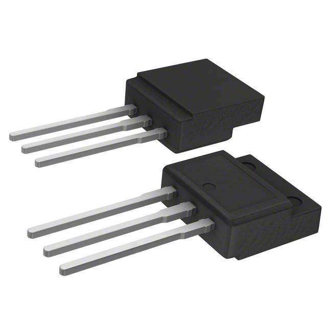
| 封装/外壳 | TO-251-3 短引线,IPak,TO-251AA |
| 封装/箱体 | IPAK-3 |
| 工厂包装数量 | 75 |
| 晶体管极性 | N-Channel |
| 最大工作温度 | + 175 C |
| 最小工作温度 | - 55 C |
| 标准包装 | 75 |
| 漏源极电压(Vdss) | 60V |
| 电流-连续漏极(Id)(25°C时) | 11A (Tc) |
| 系列 | RFD3055 |
| 通道模式 | Enhancement |
| 配置 | Single |
| 零件号别名 | RFD3055LE_NL |


- 商务部:美国ITC正式对集成电路等产品启动337调查
- 曝三星4nm工艺存在良率问题 高通将骁龙8 Gen1或转产台积电
- 太阳诱电将投资9.5亿元在常州建新厂生产MLCC 预计2023年完工
- 英特尔发布欧洲新工厂建设计划 深化IDM 2.0 战略
- 台积电先进制程称霸业界 有大客户加持明年业绩稳了
- 达到5530亿美元!SIA预计今年全球半导体销售额将创下新高
- 英特尔拟将自动驾驶子公司Mobileye上市 估值或超500亿美元
- 三星加码芯片和SET,合并消费电子和移动部门,撤换高东真等 CEO
- 三星电子宣布重大人事变动 还合并消费电子和移动部门
- 海关总署:前11个月进口集成电路产品价值2.52万亿元 增长14.8%


.jpg)

PDF Datasheet 数据手册内容提取
Is Now Part of To learn more about ON Semiconductor, please visit our website at www.onsemi.com Please note: As part of the Fairchild Semiconductor integration, some of the Fairchild orderable part numbers will need to change in order to meet ON Semiconductor’s system requirements. Since the ON Semiconductor product management systems do not have the ability to manage part nomenclature that utilizes an underscore (_), the underscore (_) in the Fairchild part numbers will be changed to a dash (-). This document may contain device numbers with an underscore (_). Please check the ON Semiconductor website to verify the updated device numbers. The most current and up-to-date ordering information can be found at www.onsemi.com. Please email any questions regarding the system integration to Fairchild_questions@onsemi.com. ON Semiconductor and the ON Semiconductor logo are trademarks of Semiconductor Components Industries, LLC dba ON Semiconductor or its subsidiaries in the United States and/or other countries. ON Semiconductor owns the rights to a number of patents, trademarks, copyrights, trade secrets, and other intellectual property. A listing of ON Semiconductor’s product/patent coverage may be accessed at www.onsemi.com/site/pdf/Patent-Marking.pdf. ON Semiconductor reserves the right to make changes without further notice to any products herein. ON Semiconductor makes no warranty, representation or guarantee regarding the suitability of its products for any particular purpose, nor does ON Semiconductor assume any liability arising out of the application or use of any product or circuit, and specifically disclaims any and all liability, including without limitation special, consequential or incidental damages. Buyer is responsible for its products and applications using ON Semiconductor products, including compliance with all laws, regulations and safety requirements or standards, regardless of any support or applications information provided by ON Semiconductor. “Typical” parameters which may be provided in ON Semiconductor data sheets and/or specifications can and do vary in different applications and actual performance may vary over time. All operating parameters, including “Typicals” must be validated for each customer application by customer’s technical experts. ON Semiconductor does not convey any license under its patent rights nor the rights of others. ON Semiconductor products are not designed, intended, or authorized for use as a critical component in life support systems or any FDA Class 3 medical devices or medical devices with a same or similar classification in a foreign jurisdiction or any devices intended for implantation in the human body. Should Buyer purchase or use ON Semiconductor products for any such unintended or unauthorized application, Buyer shall indemnify and hold ON Semiconductor and its officers, employees, subsidiaries, affiliates, and distributors harmless against all claims, costs, damages, and expenses, and reasonable attorney fees arising out of, directly or indirectly, any claim of personal injury or death associated with such unintended or unauthorized use, even if such claim alleges that ON Semiconductor was negligent regarding the design or manufacture of the part. ON Semiconductor is an Equal Opportunity/Affirmative Action Employer. This literature is subject to all applicable copyright laws and is not for resale in any manner.
RFD3055LE, RFD3055LESM Data Sheet September 2013 N-Channel Logic Level Power MOSFET Features 60V, 11A, 107 mΩ • 11A, 60V These N-Channel enhancement-mode power MOSFETs are • r = 0.107Ω DS(ON) manufactured using the latest manufacturing process technology. This process, which uses feature sizes • Temperature Compensating PSPICE® Model approaching those of LSI circuits, gives optimum utilization • Peak Current vs Pulse Width Curve of silicon, resulting in outstanding performance. They were • UIS Rating Curve designed for use in applications such as switching regulators, switching converters, motor drivers and relay • Related Literature drivers. These transistors can be operated directly from - TB334 “Guidelines for Soldering Surface Mount integrated circuits. Components to PC Boards” Formerly developmental type TA49158. Symbol Ordering Information D PART NUMBER PACKAGE BRAND RFD3055LE TO-251AA F3055L G RFD3055LESM9A TO-252AA F3055L S Packaging JEDEC TO-251AA JEDEC TO-252AA SOURCE DRAIN (FLANGE) DRAIN GATE GATE DRAIN (FLANGE) SOURCE ©2002 Fairchild Semiconductor Corporation RFD3055LE, RFD3055LESM Rev. C0
RFD3055LE, RFD3055LESM Absolute Maximum Ratings TC = 25oC, Unless Otherwise Specified RFD3055LE, RFD3055LESM9A UNITS Drain to Source Voltage (Note 1). . . . . . . . . . . . . . . . . . . . . . . . . . . . . . . . . . . . VDSS 60 V Drain to Gate Voltage (RGS = 20kΩ) (Note 1). . . . . . . . . . . . . . . . . . . . . . . . . . VDGR 60 V Gate to Source Voltage . . . . . . . . . . . . . . . . . . . . . . . . . . . . . . . . . . . . . . . . . . . . .VGS ±16 V Continuous Drain Current . . . . . . . . . . . . . . . . . . . . . . . . . . . . . . . . . . . . . . . . . . . . ID 11 A Pulsed Drain Current (Note 3) . . . . . . . . . . . . . . . . . . . . . . . . . . . . . . . . . . . . . .IDM Refer to Peak Current Curve Single Pulse Avalanche Rating . . . . . . . . . . . . . . . . . . . . . . . . . . . . . . . . . . . . . . .EAS Refer to UIS Curve Power Dissipation . . . . . . . . . . . . . . . . . . . . . . . . . . . . . . . . . . . . . . . . . . . . . . . . . .PD 38 W Derate Above 25oC . . . . . . . . . . . . . . . . . . . . . . . . . . . . . . . . . . . . . . . . . . . . . . . . . 0.25 W/oC Operating and Storage Temperature . . . . . . . . . . . . . . . . . . . . . . . . . . . . . . .TJ, TSTG -55 to 175 oC Maximum Temperature for Soldering Leads at 0.063in (1.6mm) from Case for 10s. . . . . . . . . . . . . . . . . . . . . . . . . . . .TL 300 oC Package Body for 10s, See Techbrief 334 . . . . . . . . . . . . . . . . . . . . . . . . . . . . Tpkg 260 oC CAUTION: Stresses above those listed in “Absolute Maximum Ratings” may cause permanent damage to the device. This is a stress only rating and operation of the device at these or any other conditions above those indicated in the operational sections of this specification is not implied. NOTE: 1. TJ = 25oC to 150oC. Electrical Specifications TC = 25oC, Unless Otherwise Specified PARAMETER SYMBOL TEST CONDITIONS MIN TYP MAX UNITS Drain to Source Breakdown Voltage BVDSS ID = 250µA, VGS = 0V 60 - - V Gate Threshold Voltage VGS(TH) VGS = VDS, ID = 250µA 1 - 3 V Zero Gate Voltage Drain Current IDSS VDS = 55V, VGS = 0V - - 1 µA VDS = 50V, VGS = 0V, TC = 150oC - - 250 µA Gate to Source Leakage Current IGSS VGS = ±16V - - ±100 nA Drain to Source On Resistance (Note 2) rDS(ON) ID = 8A, VGS = 5V (Figure 11) - - 0.107 Ω Turn-On Time tON VDD ≈ 30V, ID = 8A, - - 170 ns Turn-On Delay Time td(ON) VGS = 4.5V, RGS = 32Ω - 8 - ns (Figures 10, 18, 19) Rise Time tr - 105 - ns Turn-Off Delay Time td(OFF) - 22 - ns Fall Time tf - 39 - ns Turn-Off Time tOFF - - 92 ns Total Gate Charge Qg(TOT) VGS = 0V to 10V VDD = 30V, ID = 8A, - 9.4 11.3 nC Gate Charge at 5V Qg(5) VGS = 0V to 5V Ig(REF) = 1.0mA - 5.2 6.2 nC (Figures 20, 21) Threshold Gate Charge Qg(TH) VGS = 0V to 1V - 0.36 0.43 nC Input Capacitance CISS VDS = 25V, VGS = 0V, f = 1MHz - 350 - pF (Figure 14) Output Capacitance COSS - 105 - pF Reverse Transfer Capacitance CRSS - 23 - pF Thermal Resistance Junction to Case RθJC - - 3.94 oC/W Thermal Resistance Junction to Ambient RθJA TO-220AB - - 62 oC/W TO-251AA, TO-252AA - - 100 oC/W Source to Drain Diode Specifications PARAMETER SYMBOL TEST CONDITIONS MIN TYP MAX UNITS Source to Drain Diode Voltage VSD ISD = 8A - 1.25 V Diode Reverse Recovery Time trr ISD = 8A, dISD/dt = 100A/µs - 66 ns NOTES: 2. Pulse Test: Pulse Width ≤ 300ms, Duty Cycle ≤ 2%. 3. Repetitive Rating: Pulse Width limited by max junction temperature. See Transient Thermal Impedance Curve (Figure 3) and Peak Current Capability Curve (Figure 5). ©2002 Fairchild Semiconductor Corporation RFD3055LE, RFD3055LESM Rev. C0
RFD3055LE, RFD3055LESM Typical Performance Curves Unless Otherwise Specified 1.2 15 R E LI 1.0 MULTIP 0.8 NT (A) 10 VGS = 10V N RE TIO 0.6 UR VGS = 4.5V A C DISSIP 0.4 DRAIN 5 WER 0.2 I, D O P 0 0 00 25 50 75 100 125 150 175 25 50 75 100 125 150 175 TC, CASE TEMPERATURE (oC) TC, CASE TEMPERATURE (oC) FIGURE 1. NORMALIZED POWER DISSIPATION vs CASE FIGURE 2. MAXIMUM CONTINUOUS DRAIN CURRENT vs TEMPERATURE CASE TEMPERATURE 2 DUTY CYCLE - DESCENDING ORDER 1 0.5 0.2 E 0.1 D C 0.05 ZE AN 0.02 MALI MPED 0.01 PDM OR L I 0.1 N A Z, θJCHERM t1t2 T NOTES: SINGLE PULSE DUTY FACTOR: D = t1/t2 PEAK TJ = PDM x ZθJC x RθJC + TC 0.01 10-5 10-4 10-3 10-2 10-1 100 101 t, RECTANGULAR PULSE DURATION (s) FIGURE 3. NORMALIZED TRANSIENT THERMAL IMPEDANCE 100 200 TC = 25oC FOR TEMPERATURES A) A) 100 ABOVE 25oC DERATE PEAK NT ( 10 100µs NT ( CURRENT AS FOLLOWS: RE RE I = I25 175 - TC R R 150 U U AIN C AORPEEAR AMTAIOYN B IEN THIS 1ms AK C R 1 LIMITED BY rDS(ON) E , DD 10ms , PM VGS = 5V I SINGLE PULSE ID TJ = MAX RATED TC = 25oC TMRAAYN LSIMCIOTN CDUURCRTEANNTCE 0.1 IN THIS REGION 10 1 10 100 200 10-5 10-4 10-3 10-2 10-1 100 101 VDS, DRAIN TO SOURCE VOLTAGE (V) t, PULSE WIDTH (s) FIGURE 4. FORWARD BIAS SAFE OPERATING AREA FIGURE 5. PEAK CURRENT CAPABILITY ©2002 Fairchild Semiconductor Corporation RFD3055LE, RFD3055LESM Rev. C0
RFD3055LE, RFD3055LESM Typical Performance Curves Unless Otherwise Specified (Continued) 100 15 If R = 0 VGS = 10V tAV = (L)(IAS)/(1.3*RATED BVDSS - VDD) ENT (A) ItfA RV =≠ (0L/R)ln[(IAS*R)/(1.3*RATED BVDSS - VDD) +1] T (A) 12 VGS = 5V VGS = 4V R N UR STARTING TJ = 25oC RE 9 E C 10 UR VGS = 3.5V H C LANC STARTING TJ = 150oC RAIN 6 PULSE DURATION = 80µs , AVAS I, DD 3 DUTY CYCLE = 0.5% MAX A I 1 TC = 25oC VGS = 3V 0 0.001 0.01 0.1 1 10 0 1 2 3 4 tAV, TIME IN AVALANCHE (ms) VDS, DRAIN TO SOURCE VOLTAGE (V) NOTE: Refer to Fairchild Application Notes AN9321 and AN9322 FIGURE 6. UNCLAMPED INDUCTIVE SWITCHING FIGURE 7. SATURATION CHARACTERISTICS 15 150 PULSE DURATION = 80µs PULSE DURATION = 80µs DUTY CYCLE = 0.5% MAX ID = 3A ID = 11A DUTY CYCLE = 0.5% MAX 12 VDD = 15V CE TC = 25oC A) URΩm) ID = 5A URRENT ( 9 AIN TO SOSTANCE ( 120 N C 6 TJ = 25oC DRESI I DRAID, 3 TJ = 175oC r, DS(ON)ON R 90 TJ = -55oC 0 60 2 3 4 5 2 4 6 8 10 VGS, GATE TO SOURCE VOLTAGE (V) VGS, GATE TO SOURCE VOLTAGE (V) FIGURE 8. TRANSFER CHARACTERISTICS FIGURE 9. DRAIN TO SOURCE ON RESISTANCE vs GATE VOLTAGE AND DRAIN CURRENT 150 2.5 VGS = 4.5V, VDD = 30V, ID = 8A E PULSE DURATION = 80µs C DUTY CYCLE = 0.5% MAX R tr U E (ns) 100 TO SOCE2.0 M N N G TI RAISTA1.5 CHIN tf ED DRESI SWIT 50 td(OFF) MALIZON 1.0 R td(ON) NO VGS = 10V, ID = 11A 0.5 0 -80 -40 0 40 80 120 160 200 0 10 20 30 40 50 RGS, GATE TO SOURCE RESISTANCE (Ω) TJ, JUNCTION TEMPERATURE (oC) FIGURE 10. SWITCHING TIME vs GATE RESISTANCE FIGURE 11. NORMALIZED DRAIN TO SOURCE ON RESISTANCE vs JUNCTION TEMPERATURE ©2002 Fairchild Semiconductor Corporation RFD3055LE, RFD3055LESM Rev. C0
RFD3055LE, RFD3055LESM Typical Performance Curves Unless Otherwise Specified (Continued) 1.2 1.2 VGS = VDS, ID = 250µA E ID = 250µA C R NORMALIZED GATETHRESHOLD VOLTAGE01..80 MALIZED DRAIN TO SOU BREAKDOWN VOLTAGE11..01 R O N 0.6 0.9 -80 -40 0 40 80 120 160 200 -80 -40 0 40 80 120 160 200 TJ, JUNCTION TEMPERATURE (oC) TJ, JUNCTION TEMPERATURE (oC) FIGURE 12. NORMALIZED GATE THRESHOLD VOLTAGE vs FIGURE 13. NORMALIZED DRAIN TO SOURCE BREAKDOWN JUNCTION TEMPERATURE VOLTAGE vs JUNCTION TEMPERATURE 1000 10 V) VDD = 30V CISS = CGS + CGD E ( G 8 A F) LT p O TANCE ( 100 COSS ≅ CDS + CGD URCE V 6 PACI O SO 4 WAVEFORMS IN CA E T DESCENDING ORDER: C, AT 2 ID = 11A VGS = 0V, f = 1MHz CRSS = CGD V, GGS IIDD == 35AA 10 0 0.1 1 10 60 0 2 4 6 8 10 VDS, DRAIN TO SOURCE VOLTAGE (V) Qg, GATE CHARGE (nC) NOTE: Refer to Fairchild Application Notes AN7254 and AN7260. FIGURE 14. CAPACITANCE vs DRAIN TO SOURCE VOLTAGE FIGURE 15. NORMALIZED SWITCHING WAVEFORMS FOR CONSTANT GATE CURRENT Test Circuits and Waveforms VDS BVDSS L tP VDS RVAERQYU ItRP ETDO POEBATKA IINAS RG +VDD IAS VDD VGS - DUT tP 0V IAS 0 0.01Ω tAV FIGURE 16. UNCLAMPED ENERGY TEST CIRCUIT FIGURE 17. UNCLAMPED ENERGY WAVEFORMS ©2002 Fairchild Semiconductor Corporation RFD3055LE, RFD3055LESM Rev. C0
RFD3055LE, RFD3055LESM Test Circuits and Waveforms (Continued) tON tOFF td(ON) td(OFF) VDS tr tf VDS 90% 90% VGS RL + 10% 10% VDD 0 - DUT 90% RGS VGS 50% 50% PULSE WIDTH VGS 0 10% FIGURE 18. SWITCHING TEST CIRCUIT FIGURE 19. RESISTIVE SWITCHING WAVEFORMS VDS RL VDD Qg(TOT) VDS VGS = 20V VGS + Qg(10) OR Qg(5) VL2G SD E= V1I0CVE FSOR -VDD VGS VVGGSS == 51V0V FOR DUT VGS = 2V VGS = 1V FOR L2 DEVICES Ig(REF) 0 L2 DEVICES Qg(TH) Ig(REF) 0 FIGURE 20. GATE CHARGE TEST CIRCUIT FIGURE 21. GATE CHARGE WAVEFORMS ©2002 Fairchild Semiconductor Corporation RFD3055LE, RFD3055LESM Rev. C0
RFD3055LE, RFD3055LESM PSPICE Electrical Model .SUBCKT RFD3055LE 2 1 3 ; rev 1/30/95 CA 12 8 3.9e-9 CB 15 14 4.9e-9 CIN 6 8 3.25e-10 DBODY 7 5 DBODYMOD LDRAIN DBREAK 5 11 DBREAKMOD DPLCAP 5 DRAIN DPLCAP 10 5 DPLCAPMOD 2 10 RLDRAIN EBREAK 11 7 17 18 67.8 RSLC1 EDS 14 8 5 8 1 51 DBREAK EGS 13 8 6 8 1 RSLC2 + 5 ESG 6 10 6 8 1 51 ESLC 11 EVTHRES 6 21 19 8 1 - EVTEMP 20 6 18 22 1 - 50 + 6 RDRAIN 17 DBODY ESG EBREAK 18 IT 8 17 1 +8 EVTHRES 16 - LDRAIN 2 5 1.0e-9 LGATE EVTEMP + 189 - 21 MWEAK LGATE 1 9 5.42e-9 GATE RGATE + 18 - 6 LSOURCE 3 7 2.57e-9 1 22 MMED 9 20 MSTRO MMED 16 6 8 8 MMEDMOD RLGATE MSTRO 16 6 8 8 MSTROMOD LSOURCE MWEAK 16 21 8 8 MWEAKMOD CIN 8 7 SOU3RCE RBREAK 17 18 RBREAKMOD 1 RSOURCE RLSOURCE RDRAIN 50 16 RDRAINMOD 3.7e-2 RGATE 9 20 3.37 S1A S2A RLDRAIN 2 5 10 12 13 14 15 RBREAK 17 18 RLGATE 1 9 54.2 8 13 RLSOURCE 3 7 25.7 S1B S2B RVTEMP RSLC1 5 51 RSLCMOD 1e-6 RSLC2 5 50 1e3 CA 13 CB 19 RSOURCE 8 7 RSOURCEMOD 2.50e-2 ++ + 14 IT - RVTHRES 22 8 RVTHRESMOD 1 6 5 VBAT RVTEMP 18 19 RVTEMPMOD 1 EGS 8 EDS 8 + -- - 8 S1A 6 12 13 8 S1AMOD 22 S1B 13 12 13 8 S1BMOD RVTHRES S2A 6 15 14 13 S2AMOD S2B 13 15 14 13 S2BMOD VBAT 22 19 DC 1 ESLC 51 50 VALUE={(V(5,51)/ABS(V(5,51)))*(PWR(V(5,51)/(1e-6*30),3))} .MODEL DBODYMOD D (IS = 1.75e-13 RS = 1.75e-2 TRS1 = 1e-4 TRS2 = 5e-6 CJO = 5.9e-10 TT = 5.45e-8 N = 1.03 M = 0.6) .MODEL DBREAKMOD D (RS = 6.50e-1 TRS1 = 1.25e-4 TRS2 = 1.34e-6) .MODEL DPLCAPMOD D (CJO = 3.21e-10 IS = 1e-30 N = 10 M = 0.81) .MODEL MMEDMOD NMOS (VTO = 2.02 KP = .83 IS = 1e-30 N = 10 TOX = 1 L = 1u W = 1u RG = 3.37) .MODEL MSTROMOD NMOS (VTO = 2.39 KP = 14 IS = 1e-30 N = 10 TOX = 1 L = 1u W = 1u) .MODEL MWEAKMOD NMOS (VTO = 1.78 KP = 0.02 IS = 1e-30 N = 10 TOX = 1 L = 1u W = 1u RG = 33.7 RS = 0.1) .MODEL RBREAKMOD RES (TC1 = 1.06e-3 TC2 = 0) .MODEL RDRAINMOD RES (TC1 = 1.23e-2 TC2 = 2.58e-5) .MODEL RSLCMOD RES (TC1 = 0 TC2 = 0) .MODEL RSOURCEMOD RES (TC1 = 1e-3 TC2 = 0) .MODEL RVTHRESMOD RES (TC1 = -2.19e-3 TC2 = -4.97e-6) .MODEL RVTEMPMOD RES (TC1 = -1.6e-3 TC2 = 1e-7) .MODEL S1AMOD VSWITCH (RON = 1e-5 ROFF = 0.1 VON = -4 VOFF= -2.5) .MODEL S1BMOD VSWITCH (RON = 1e-5 ROFF = 0.1 VON = -2.5 VOFF= -4) .MODEL S2AMOD VSWITCH (RON = 1e-5 ROFF = 0.1 VON = -0.5 VOFF= 0) .MODEL S2BMOD VSWITCH (RON = 1e-5 ROFF = 0.1 VON = 0 VOFF= -0.5) .ENDS For further discussion of the PSPICE model, consult A New PSPICE Sub-Circuit for the Power MOSFET Featuring Global Temperature Options; IEEE Power Electronics Specialist Conference Records, 1991, written by William J. Hepp and C. Frank Wheatley. ©2002 Fairchild Semiconductor Corporation RFD3055LE, RFD3055LESM Rev. C0
RFD3055LE, RFD3055LESM TRADEMARKS The following includes registered and unregistered trademarks and service marks, owned by Fairchild Semiconductor and/or its global subsidiaries, and is not intended to be an exhaustive list of all such trademarks. AccuPower™ F-PFS™ Sync-Lock™ AX-CAP®* FRFET® ® ®* BitSiC™ Global Power ResourceSM PowtmerTrench® Build it Now™ GreenBridge™ PowerXS™ TinyBoost® CCoorreePPOLUWSE™R™ GGrreeeenn FFPPSS™™ e-Series™ PQrFoEgTra®mmable Active Droop™ TinyBuck® TinyCalc™ CROSSVOLT™ Gmax™ QS™ TinyLogic® CTL™ GTO™ Quiet Series™ TINYOPTO™ Current Transfer Logic™ IntelliMAX™ RapidConfigure™ DEUXPEED® ISOPLANAR™ ™ TinyPower™ TinyPWM™ Dual Cool™ Marking Small Speakers Sound Louder EcoSPARK® and Better™ Saving our world, 1mW/W/kW at a time™ TinyWire™ TranSiC™ EfficentMax™ MegaBuck™ SignalWise™ TriFault Detect™ ESBC™ MICROCOUPLER™ SmartMax™ TRUECURRENT®* MicroFET™ SMART START™ ® SerDes™ MicroPak™ Solutions for Your Success™ Fairchild® MicroPak2™ SPM® FFAaiCrcTh iQldu Sieet mSiecroiensd™uctor® MMiollteiorDnMrivaex™™ SSTupEeArLFTEHT™® UHC® FACT® mWSaver® SuperSOT™-3 Ultra FRFET™ FAST® OptoHiT™ SuperSOT™-6 UniFET™ FastvCore™ OPTOLOGIC® SuperSOT™-8 VCX™ FETBench™ OPTOPLANAR® SupreMOS® VisualMax™ FPS™ SyncFET™ VoltagePlus™ XS™ *Trademarks of System General Corporation, used under license by Fairchild Semiconductor. DISCLAIMER FAIRCHILD SEMICONDUCTOR RESERVES THE RIGHT TO MAKE CHANGES WITHOUT FURTHER NOTICE TO ANY PRODUCTS HEREIN TO IMPROVE RELIABILITY, FUNCTION, OR DESIGN. FAIRCHILD DOES NOT ASSUME ANY LIABILITY ARISING OUT OF THE APPLICATION OR USE OF ANY PRODUCT OR CIRCUIT DESCRIBED HEREIN; NEITHER DOES IT CONVEY ANY LICENSE UNDER ITS PATENT RIGHTS, NOR THE RIGHTS OF OTHERS. THESE SPECIFICATIONS DO NOT EXPAND THE TERMS OF FAIRCHILD’S WORLDWIDE TERMS AND CONDITIONS, SPECIFICALLY THE WARRANTY THEREIN, WHICH COVERS THESE PRODUCTS. LIFE SUPPORT POLICY FAIRCHILD’S PRODUCTS ARE NOT AUTHORIZED FOR USE AS CRITICAL COMPONENTS IN LIFE SUPPORT DEVICES OR SYSTEMS WITHOUT THE EXPRESS WRITTEN APPROVAL OF FAIRCHILD SEMICONDUCTOR CORPORATION. As used here in: 1. Life support devices or systems are devices or systems which, (a) are 2. A critical component in any component of a life support, device, or intended for surgical implant into the body or (b) support or sustain life, system whose failure to perform can be reasonably expected to cause and (c) whose failure to perform when properly used in accordance with the failure of the life support device or system, or to affect its safety or instructions for use provided in the labeling, can be reasonably effectiveness. expected to result in a significant injury of the user. ANTI-COUNTERFEITING POLICY Fairchild Semiconductor Corporation’s Anti-Counterfeiting Policy. Fairchild’s Anti-Counterfeiting Policy is also stated on our external website, www.Fairchildsemi.com, under Sales Support. Counterfeiting of semiconductor parts is a growing problem in the industry. All manufactures of semiconductor products are experiencing counterfeiting of their parts. Customers who inadvertently purchase counterfeit parts experience many problems such as loss of brand reputation, substandard performance, failed application, and increased cost of production and manufacturing delays. Fairchild is taking strong measures to protect ourselves and our customers from the proliferation of counterfeit parts. Fairchild strongly encourages customers to purchase Fairchild parts either directly from Fairchild or from Authorized Fairchild Distributors who are listed by country on our web page cited above. Products customers buy either from Fairchild directly or from Authorized Fairchild Distributors are genuine parts, have full traceability, meet Fairchild’s quality standards for handing and storage and provide access to Fairchild’s full range of up-to-date technical and product information. Fairchild and our Authorized Distributors will stand behind all warranties and will appropriately address and warranty issues that may arise. Fairchild will not provide any warranty coverage or other assistance for parts bought from Unauthorized Sources. Fairchild is committed to combat this global problem and encourage our customers to do their part in stopping this practice by buying direct or from authorized distributors. PRODUCT STATUS DEFINITIONS Definition of Terms Datasheet Identification Product Status Definition Datasheet contains the design specifications for product development. Specifications Advance Information Formative / In Design may change in any manner without notice. Datasheet contains preliminary data; supplementary data will be published at a later Preliminary First Production date. Fairchild Semiconductor reserves the right to make changes at any time without notice to improve design. Datasheet contains final specifications. Fairchild Semiconductor reserves the right to No Identification Needed Full Production make changes at any time without notice to improve the design. Datasheet contains specifications on a product that is discontinued by Fairchild Obsolete Not In Production Semiconductor. The datasheet is for reference information only. Rev. I66 ©2002 Fairchild Semiconductor Corporation RFD3055LE, RFD3055LESM Rev. C0
ON Semiconductor and are trademarks of Semiconductor Components Industries, LLC dba ON Semiconductor or its subsidiaries in the United States and/or other countries. ON Semiconductor owns the rights to a number of patents, trademarks, copyrights, trade secrets, and other intellectual property. A listing of ON Semiconductor’s product/patent coverage may be accessed at www.onsemi.com/site/pdf/Patent−Marking.pdf. ON Semiconductor reserves the right to make changes without further notice to any products herein. ON Semiconductor makes no warranty, representation or guarantee regarding the suitability of its products for any particular purpose, nor does ON Semiconductor assume any liability arising out of the application or use of any product or circuit, and specifically disclaims any and all liability, including without limitation special, consequential or incidental damages. Buyer is responsible for its products and applications using ON Semiconductor products, including compliance with all laws, regulations and safety requirements or standards, regardless of any support or applications information provided by ON Semiconductor. “Typical” parameters which may be provided in ON Semiconductor data sheets and/or specifications can and do vary in different applications and actual performance may vary over time. All operating parameters, including “Typicals” must be validated for each customer application by customer’s technical experts. ON Semiconductor does not convey any license under its patent rights nor the rights of others. ON Semiconductor products are not designed, intended, or authorized for use as a critical component in life support systems or any FDA Class 3 medical devices or medical devices with a same or similar classification in a foreign jurisdiction or any devices intended for implantation in the human body. Should Buyer purchase or use ON Semiconductor products for any such unintended or unauthorized application, Buyer shall indemnify and hold ON Semiconductor and its officers, employees, subsidiaries, affiliates, and distributors harmless against all claims, costs, damages, and expenses, and reasonable attorney fees arising out of, directly or indirectly, any claim of personal injury or death associated with such unintended or unauthorized use, even if such claim alleges that ON Semiconductor was negligent regarding the design or manufacture of the part. ON Semiconductor is an Equal Opportunity/Affirmative Action Employer. This literature is subject to all applicable copyright laws and is not for resale in any manner. PUBLICATION ORDERING INFORMATION LITERATURE FULFILLMENT: N. American Technical Support: 800−282−9855 Toll Free ON Semiconductor Website: www.onsemi.com Literature Distribution Center for ON Semiconductor USA/Canada 19521 E. 32nd Pkwy, Aurora, Colorado 80011 USA Europe, Middle East and Africa Technical Support: Order Literature: http://www.onsemi.com/orderlit Phone: 303−675−2175 or 800−344−3860 Toll Free USA/Canada Phone: 421 33 790 2910 Fax: 303−675−2176 or 800−344−3867 Toll Free USA/Canada Japan Customer Focus Center For additional information, please contact your local Email: orderlit@onsemi.com Phone: 81−3−5817−1050 Sales Representative © Semiconductor Components Industries, LLC www.onsemi.com www.onsemi.com 1
Mouser Electronics Authorized Distributor Click to View Pricing, Inventory, Delivery & Lifecycle Information: O N Semiconductor: RFD3055LE