ICGOO在线商城 > 分立半导体产品 > 晶体管 - FET,MOSFET - 单 > IRF9530NSTRLPBF
/IRF9530NSTRLPBF.jpg)
 Datasheet下载
- 型号: IRF9530NSTRLPBF
- 制造商: International Rectifier
- 库位|库存: xxxx|xxxx
- 要求:
| 数量阶梯 | 香港交货 | 国内含税 |
| +xxxx | $xxxx | ¥xxxx |
查看当月历史价格
查看今年历史价格
IRF9530NSTRLPBF产品简介:
ICGOO电子元器件商城为您提供IRF9530NSTRLPBF由International Rectifier设计生产,在icgoo商城现货销售,并且可以通过原厂、代理商等渠道进行代购。 IRF9530NSTRLPBF价格参考¥2.88-¥3.13。International RectifierIRF9530NSTRLPBF封装/规格:晶体管 - FET,MOSFET - 单, P-Channel 100V 14A (Tc) 3.8W (Ta), 79W (Tc) Surface Mount D2PAK。您可以下载IRF9530NSTRLPBF参考资料、Datasheet数据手册功能说明书,资料中有IRF9530NSTRLPBF 详细功能的应用电路图电压和使用方法及教程。
Infineon Technologies 的 IRF9530NSTRLPBF 是一款P沟道MOSFET,属于高性能功率晶体管,广泛应用于需要高效开关和功率控制的场景。其主要应用场景包括:

1. 电源管理:常用于DC-DC转换器、电压调节模块(VRM)和开关电源(SMPS)中,实现高效的电能转换与稳定输出。

2. 负载开关:适用于电池供电设备中的电源开关控制,如便携式电子设备(笔记本电脑、平板、移动电源),可有效防止反向电流并实现低功耗待机。

3. 电机驱动:在小型直流电机或步进电机的H桥驱动电路中作为高端或低端开关,用于家电、电动工具及工业控制系统。

4. 逆变器与UPS系统:用于不间断电源(UPS)和逆变器中的功率切换,提升系统响应速度与能效。

5. 汽车电子:符合AEC-Q101标准,适合车载环境,可用于车身控制模块、车灯驱动、继电器替代等应用,具备良好的温度稳定性和可靠性。

IRF9530NSTRLPBF采用表面贴装封装(如DPAK),具有低导通电阻(RDS(on))、高耐压(-100V)和良好热性能,适合紧凑型设计与高密度电路板布局。其环保无铅设计也符合RoHS标准,适用于注重环保的工业与消费类电子产品。
| 参数 | 数值 |
| 产品目录 | |
| 描述 | MOSFET P-CH 100V 14A D2PAKMOSFET MOSFT PCh -100V -14A 200mOhm 38.7nC |
| 产品分类 | FET - 单分离式半导体 |
| FET功能 | 标准 |
| FET类型 | MOSFET P 通道,金属氧化物 |
| Id-连续漏极电流 | - 14 A |
| 品牌 | International Rectifier |
| 产品手册 | |
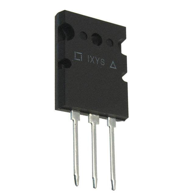
| 产品图片 |
|
| rohs | 符合RoHS无铅 / 符合限制有害物质指令(RoHS)规范要求 |
| 产品系列 | 晶体管,MOSFET,International Rectifier IRF9530NSTRLPBFHEXFET® |
| 数据手册 | |
| 产品型号 | IRF9530NSTRLPBF |
| PCN组件/产地 | |
| Pd-PowerDissipation | 3.8 W |
| Pd-功率耗散 | 3.8 W |
| Qg-GateCharge | 38.7 nC |
| Qg-栅极电荷 | 38.7 nC |
| RdsOn-漏源导通电阻 | 200 mOhms |
| Vds-漏源极击穿电压 | - 100 V |
| Vgs-Gate-SourceBreakdownVoltage | 20 V |
| Vgs-栅源极击穿电压 | 20 V |
| 不同Id时的Vgs(th)(最大值) | 4V @ 250µA |
| 不同Vds时的输入电容(Ciss) | 760pF @ 25V |
| 不同Vgs时的栅极电荷(Qg) | 58nC @ 10V |
| 不同 Id、Vgs时的 RdsOn(最大值) | 200 毫欧 @ 8.4A,10V |
| 产品培训模块 | http://www.digikey.cn/PTM/IndividualPTM.page?site=cn&lang=zhs&ptm=26250 |
| 产品种类 | MOSFET |
| 供应商器件封装 | D2PAK |
| 其它名称 | IRF9530NSTRLPBFDKR |
| 功率-最大值 | 3.8W |
| 功率耗散 | 3.8 W |
| 包装 | Digi-Reel® |
| 商标 | International Rectifier |
| 安装类型 | 表面贴装 |
| 安装风格 | SMD/SMT |
| 导通电阻 | 200 mOhms |
| 封装 | Reel |
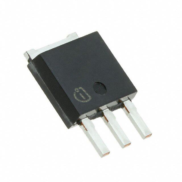
| 封装/外壳 | TO-263-3,D²Pak(2 引线+接片),TO-263AB |
| 封装/箱体 | D2PAK-2 |
| 工厂包装数量 | 800 |
| 晶体管极性 | P-Channel |
| 栅极电荷Qg | 38.7 nC |
| 标准包装 | 1 |
| 汲极/源极击穿电压 | - 100 V |
| 漏极连续电流 | - 14 A |
| 漏源极电压(Vdss) | 100V |
| 电流-连续漏极(Id)(25°C时) | 14A (Tc) |
| 闸/源击穿电压 | 20 V |


PDF Datasheet 数据手册内容提取
IRF9530NSPbF IRF9530NLPbF Benefits HEXFET® Power MOSFET Advanced Process Technology Surface Mount (IRF9530NS) V -100V DSS Low-profile through-hole(IRF9530NL) 175°C Operating Temperature R 0.20 DS(on) Fast Switching I -14A P-Channel D Fully Avalanche Rated Lead-Free D D Description Fifth Generation HEXFET® Power MOSFETs from International Rectifier utilize advanced processing techniques to achieve S S D extremely low on-resistance per silicon area. This benefit, G G combined with the fast switching speed and ruggedized device D2 Pak TO-262 Pak design that HEXFET power MOSFETs are well known for, IRF9530NSPbF IRF9530NLPbF provides the designer with an extremely efficient and reliable device for use in a wide variety of applications. G D S The D2Pak is a surface mount power package capable of Gate Drain Source accommodating die sizes up to HEX-4. It provides the highest power capability and the lowest possible on-resistance in any existing surface mount package. The D2Pak is suitable for high current applications because of its low internal connection resistance and can dissipate up to 2.0W in a typical surface mount application. The through-hole version (IRF9530NL) is available for low- profile applications. Standard Pack Base part number Package Type Orderable Part Number Form Quantity IRF9530NLPbF TO-262 Tube 50 IRF9530NLPbF (Obsolete) IRF9530NSPbF D2-Pak Tape and Reel Left 800 IRF9530NSTRLPbF Absolute Maximum Ratings Symbol Parameter Max. Units I @ T = 25°C Continuous Drain Current, V @ -10V -14 D C GS I @ T = 100°C Continuous Drain Current, V @ -10V -10 A D C GS I Pulsed Drain Current -56 DM P @T = 25°C Maximum Power Dissipation 3.8 W D A P @T = 25°C Maximum Power Dissipation 79 W D C Linear Derating Factor 0.53 W/°C V Gate-to-Source Voltage ± 20 V GS E Single Pulse Avalanche Energy (Thermally Limited) 250 mJ AS I Avalanche Current -8.4 A AR E Repetitive Avalanche Energy 7.9 mJ AR dv/dt Peak Diode Recovery dv/dt -5.0 V/ns T Operating Junction and -55 to + 175 J T Storage Temperature Range °C STG Soldering Temperature, for 10 seconds (1.6mm from case) 300 Mounting torque, 6-32 or M3 screw 10 lbf•in (1.1N•m) Thermal Resistance Symbol Parameter Typ. Max. Units R Junction-to-Case ––– 1.9 JC °C/W R Junction-to-Ambient ( PCB Mount, steady state) ––– 40 JA 1 2016-5-27
IRF9530NS/LPbF Electrical Characteristics @ T = 25°C (unless otherwise specified) J Parameter Min. Typ. Max. Units Conditions V Drain-to-Source Breakdown Voltage -100 ––– ––– V V = 0V, I = -250µA (BR)DSS GS D V /T Breakdown Voltage Temp. Coefficient ––– -0.11 ––– V/°C Reference to 25°C, I = -1mA (BR)DSS J D R Static Drain-to-Source On-Resistance ––– ––– 0.20 V = -10V, I = -8.4A DS(on) GS D V Gate Threshold Voltage -2.0 ––– -4.0 V V = V , I = -250µA GS(th) DS GS D gfs Forward Trans conductance 3.2 ––– ––– S V = -50V, I = -8.4A DS D ––– ––– -25 V = -100V, V = 0V I Drain-to-Source Leakage Current µA DS GS DSS ––– ––– -250 V = -80V,V = 0V,T =150°C DS GS J Gate-to-Source Forward Leakage ––– ––– -100 V = -20V I nA GS GSS Gate-to-Source Reverse Leakage ––– ––– 100 V = 20V GS Q Total Gate Charge ––– ––– 58 I = -8.4A g D Q Gate-to-Source Charge ––– ––– 8.3 nC V = -80V gs DS Q Gate-to-Drain Charge ––– ––– 32 V = -10V See Fig.6 and 13 gd GS t Turn-On Delay Time ––– 15 ––– V = -50V d(on) DD t Rise Time ––– 58 ––– I = -8.4A r ns D t Turn-Off Delay Time ––– 45 ––– R = 9.1 d(off) G t Fall Time ––– 46 ––– R = 6.2See Fig.6 f D Between lead, L Internal Source Inductance ––– 7.5 ––– nH S and center of die contact C Input Capacitance ––– 760 ––– V = 0V iss GS C Output Capacitance ––– 260 ––– pF V = -25V oss DS C Reverse Transfer Capacitance ––– 170 ––– ƒ = 1.0MHz, See Fig. 5 rss Source-Drain Ratings and Characteristics Parameter Min. Typ. Max. Units Conditions Continuous Source Current MOSFET symbol I ––– ––– -14 S (Body Diode) showing the A Pulsed Source Current integral reverse I ––– ––– -56 SM (Body Diode) p-n junction diode. V Diode Forward Voltage ––– ––– -1.6 V T = 25°C,I = -8.4A,V = 0V SD J S GS t Reverse Recovery Time ––– 130 190 ns T = 25°C ,I = -8.4A rr J F Q Reverse Recovery Charge ––– 650 970 nC di/dt = -100A/µs rr t Forward Turn-On Time Intrinsic turn-on time is negligible (turn-on is dominated by L +L ) on S D Notes: Repetitive rating; pulse width limited by max. junction temperature. (See fig. 11) starting T = 25°C, L = 7.0mH, R = 25, I = -8.4A. (See fig. 12) J G AS I -8.4A, di/dt -490A/µs, V V , T 175°C. SD DD (BR)DSS J Pulse width 300µs; duty cycle 2%. Uses IRF9530N data and test conditions. When mounted on 1" square PCB (FR-4 or G-10 Material). For recommended footprint and soldering techniques refer to application note #AN-994 2 2016-5-27
IRF9530NS/LPbF Fig. 1 Typical Output Characteristics Fig. 2 Typical Output Characteristics Fig. 3 Typical Transfer Characteristics Fig. 4 Normalized On-Resistance vs. Temperature 3 2016-5-27
IRF9530NS/LPbF Fig 5. Typical Capacitance vs. Fig 6. Typical Gate Charge vs. Drain-to-Source Voltage Gate-to-Source Voltage Fig. 7 Typical Source-to-Drain Diode Fig 8. Maximum Safe Operating Area Forward Voltage 4 2016-5-27
IRF9530NS/LPbF Fig 10a. Switching Time Test Circuit Fig 9. Maximum Drain Current vs. Case Temperature Fig 10b. Switching Time Waveforms Fig 11. Maximum Effective Transient Thermal Impedance, Junction-to-Case 5 2016-5-27
IRF9530NS/LPbF Fig 12a. Unclamped Inductive Test Circuit Fig 12c. Maximum Avalanche Energy vs. Drain Current Fig 12b. Unclamped Inductive Waveforms Fig 13b. Gate Charge Test Circuit Fig 13a. Gate Charge Waveform 6 2016-5-27
IRF9530NS/LPbF Fig 14. Peak Diode Recovery dv/dt Test Circuit for PChannel HEXFET® Power MOSFETs 7 2016-5-27
IRF9530NS/LPbF D2-Pak (TO-263AB) Package Outline (Dimensions are shown in millimeters (inches)) D2-Pak (TO-263AB) Part Marking Information THIS IS AN IRF530S WITH PART NUMBER LOT CODE 8024 INTERNATIONAL ASSEMBLED ON WW 02, 2000 RECTIFIER F530S IN THE ASSEMBLY LINE "L" LOGO DATE CODE YEAR 0 = 2000 ASSEMBLY LOT CODE WEEK 02 LINE L OR PART NUMBER INTERNATIONAL RECTIFIER F530S LOGO DATE CODE P = DESIGNATES LEAD - FREE PRODUCT (OPTIONAL) ASSEMBLY YEAR 0 = 2000 LOT CODE WEEK 02 A = ASSEMBLY SITE CODE Note: For the most current drawing please refer to Infineon’s web site www.infineon.com 8 2016-5-27
IRF9530NS/LPbF TO-262 Package Outline (Dimensions are shown in millimeters (inches) TO-262 Part Marking Information EXAMPLE: THIS IS AN IRL3103L LOT CODE 1789 PART NUMBER INTERNATIONAL ASSEMBLED ON WW 19, 1997 RECTIFIER IN THE ASSEMBLY LINE "C" LOGO DATE CODE ASSEMBLY YEAR 7 = 1997 LOT CODE WEEK 19 LINE C OR PART NUMBER INTERNATIONAL RECTIFIER LOGO DATE CODE ASSEMBLY P = DESIGNATES LEAD-FREE LOT CODE PRODUCT (OPTIONAL) YEAR 7 = 1997 WEEK 19 A = ASSEMBLY SITE CODE Note: For the most current drawing please refer to Infineon’s web site www.infineon.com 9 2016-5-27
IRF9530NS/LPbF D2-Pak (TO-263AB) Tape & Reel Information (Dimensions are shown in millimeters (inches)) TRR 1.60 (.063) 1.50 (.059) 1.60 (.063) 4.10 (.161) 3.90 (.153) 1.50 (.059) 0.368 (.0145) 0.342 (.0135) FEED DIRECTION 1.85 (.073) 11.60 (.457) 1.65 (.065) 11.40 (.449) 24.30 (.957) 15.42 (.609) 23.90 (.941) 15.22 (.601) TRL 1.75 (.069) 10.90 (.429) 1.25 (.049) 10.70 (.421) 4.72 (.136) 16.10 (.634) 4.52 (.178) 15.90 (.626) FEED DIRECTION 13.50 (.532) 27.40 (1.079) 12.80 (.504) 23.90 (.941) 4 330.00 60.00 (2.362) (14.173) MIN. MAX. 30.40 (1.197) NOTES : MAX. 1. COMFORMS TO EIA-418. 26.40 (1.039) 4 2. CONTROLLING DIMENSION: MILLIMETER. 24.40 (.961) 3. DIMENSION MEASURED @ HUB. 3 4. INCLUDES FLANGE DISTORTION @ OUTER EDGE. Note: For the most current drawing please refer to Infineon’s web site www.infineon.com 10 2016-5-27
IRF9530NS/LPbF Qualification Information† Industrial Qualification Level (per JEDEC JESD47F) †† MSL1 D2-Pak Moisture Sensitivity Level (per JEDEC J-STD-020D) †† TO-262 N/A RoHS Compliant Yes † Qualification standards can be found at Infineon’s web site www.infineon.com †† Applicable version of JEDEC standard at the time of product release. Revision History Date Comments Updated datasheet with corporate template. 5/27/2016 Added disclaimer on last page. TO-262 package was removed from ordering information since it is EOL on page 1. Trademarks of Infineon Technologies AG µHVIC™, µIPM™, µPFC™, AU‐ConvertIR™, AURIX™, C166™, CanPAK™, CIPOS™, CIPURSE™, CoolDP™, CoolGaN™, COOLiR™, CoolMOS™, CoolSET™, CoolSiC™, DAVE™, DI‐POL™, DirectFET™, DrBlade™, EasyPIM™, EconoBRIDGE™, EconoDUAL™, EconoPACK™, EconoPIM™, EiceDRIVER™, eupec™, FCOS™, GaNpowIR™, HEXFET™, HITFET™, HybridPACK™, iMOTION™, IRAM™, ISOFACE™, IsoPACK™, LEDrivIR™, LITIX™, MIPAQ™, ModSTACK™, my‐d™, NovalithIC™, OPTIGA™, Op(cid:415)MOS™, ORIGA™, PowIRaudio™, PowIRStage™, PrimePACK™, PrimeSTACK™, PROFET™, PRO‐SIL™, RASIC™, REAL3™, SmartLEWIS™, SOLID FLASH™, SPOC™, StrongIRFET™, SupIRBuck™, TEMPFET™, TRENCHSTOP™, TriCore™, UHVIC™, XHP™, XMC™ Trademarks updated November 2015 Other Trademarks All referenced product or service names and trademarks are the property of their respec(cid:415)ve owners. IMPORTANT NOTICE Edi(cid:415)on 2016‐04‐19 For further informa(cid:415)on on the product, technology, The informa(cid:415)on given in this document shall in no Published by delivery terms and condi(cid:415)ons and prices please event be regarded as a guarantee of condi(cid:415)ons or contact your nearest Infineon Technologies office Infineon Technologies AG characteris(cid:415)cs (“Beschaffenheitsgaran(cid:415)e”) . (www.infineon.com). 81726 Munich, Germany With respect to any examples, hints or any typical Please note that this product is not qualified values stated herein and/or any informa(cid:415)on © 2016 Infineon Technologies AG. regarding the applica(cid:415)on of the product, Infineon according to the AEC Q100 or AEC Q101 documents All Rights Reserved. Technologies hereby disclaims any and all of the Automo(cid:415)ve Electronics Council. warran(cid:415)es and liabili(cid:415)es of any kind, including Do you have a ques(cid:415)on about this without limita(cid:415)on warran(cid:415)es of non‐infringement WARNINGS document? of intellectual property rights of any third party. Due to technical requirements products may Email: erratum@infineon.com contain dangerous substances. For informa(cid:415)on on In addi(cid:415)on, any informa(cid:415)on given in this document the types in ques(cid:415)on please contact your nearest is subject to customer’s compliance with its Infineon Technologies office. obliga(cid:415)ons stated in this document and any Document reference applicable legal requirements, norms and Except as otherwise explicitly approved by Infineon Technologies in a wri(cid:425)en document signed by ifx1 standards concerning customer’s products and any authorized representa(cid:415)ves of Infineon Technologies, use of the product of Infineon Technologies in Infineon Technologies’ products may not be used in customer’s applica(cid:415)ons. any applica(cid:415)ons where a failure of the product or any consequences of the use thereof can reasonably The data contained in this document is exclusively be expected to result in personal injury. intended for technically trained staff. It is the responsibility of customer’s technical departments to evaluate the suitability of the product for the intended applica(cid:415)on and the completeness of the product informa(cid:415)on given in this document with respect to such applica(cid:415)on. 11 2016-5-27
Mouser Electronics Authorized Distributor Click to View Pricing, Inventory, Delivery & Lifecycle Information: I nfineon: IRF9530NSPBF IRF9530NSTRRPBF IRF9530NSTRLPBF