ICGOO在线商城 > 分立半导体产品 > 晶体管 - FET,MOSFET - 单 > IRF6655TRPBF
/IRF6655TRPBF.jpg)
 Datasheet下载
- 型号: IRF6655TRPBF
- 制造商: International Rectifier
- 库位|库存: xxxx|xxxx
- 要求:
| 数量阶梯 | 香港交货 | 国内含税 |
| +xxxx | $xxxx | ¥xxxx |
查看当月历史价格
查看今年历史价格
IRF6655TRPBF产品简介:
ICGOO电子元器件商城为您提供IRF6655TRPBF由International Rectifier设计生产,在icgoo商城现货销售,并且可以通过原厂、代理商等渠道进行代购。 IRF6655TRPBF价格参考。International RectifierIRF6655TRPBF封装/规格:晶体管 - FET,MOSFET - 单, 表面贴装 N 沟道 100V 4.2A(Ta),19A(Tc) 2.2W(Ta),42W(Tc) DIRECTFET™ SH。您可以下载IRF6655TRPBF参考资料、Datasheet数据手册功能说明书,资料中有IRF6655TRPBF 详细功能的应用电路图电压和使用方法及教程。
IRF6655TRPBF 是由 Infineon Technologies(英飞凌科技)生产的一款晶体管,属于 FET(场效应晶体管)和 MOSFET(金属氧化物半导体场效应晶体管)类别,具体为单通道设计。以下是该型号的主要应用场景:

 1. 开关电源 (SMPS)
   - IRF6655TRPBF 常用于开关电源的设计中,作为功率开关器件。其低导通电阻(Rds(on))特性能够有效降低功耗,提高效率。
   - 应用实例:适配器、充电器、DC-DC 转换器等。

 2. 电机驱动
   - 适用于小型直流电机或步进电机的驱动控制,特别是在需要高效能和低热量产生的场景中。
   - 其快速开关速度和低损耗特性使其成为电机驱动的理想选择。

 3. 电池管理系统 (BMS)
   - 在电池管理系统中,IRF6655TRPBF 可用于充放电保护、电流调节以及负载切换等功能。
   - 适合锂离子电池组或其他可充电电池的应用。

 4. LED 驱动
   - 用于高亮度 LED 的驱动电路,提供精确的电流控制和高效的能量转换。
   - 特别适合大功率 LED 照明设备。

 5. 逆变器
   - 在小型逆变器中,IRF6655TRPBF 可作为核心开关元件,实现交流与直流之间的转换。
   - 应用于太阳能微逆变器或家用应急电源系统。

 6. 负载开关
   - 在电子设备中,可用作负载开关以实现电源的快速接通和断开,同时减少漏电流。
   - 适合便携式设备如平板电脑、智能手机等。

 7. 工业自动化
   - 在工业控制领域,IRF6655TRPBF 可用于继电器替代、信号放大和功率控制等场合。
   - 例如:PLC 输出模块、传感器接口等。

 总结
IRF6655TRPBF 凭借其优异的电气性能(如低 Rds(on)、高击穿电压和快速开关能力),广泛应用于消费电子、工业控制、汽车电子及新能源等领域。它特别适合需要高效能、低热损耗和可靠性的应用环境。
| 参数 | 数值 |
| 产品目录 | |
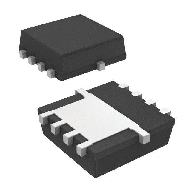
| 描述 | MOSFET N-CH 100V 4.2A DIRECTFET |
| 产品分类 | FET - 单 |
| FET功能 | 标准 |
| FET类型 | MOSFET N 通道,金属氧化物 |
| 品牌 | International Rectifier |
| 数据手册 | |
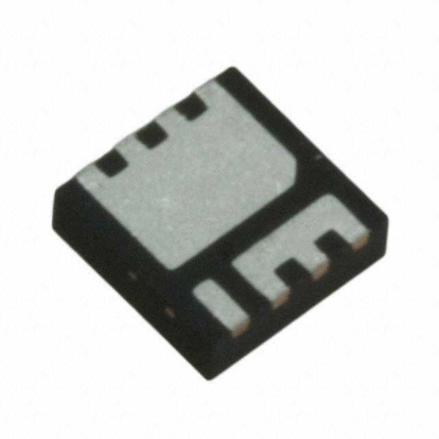
| 产品图片 |
|
| 产品型号 | IRF6655TRPBF |
| PCN其它 | |
| PCN组件/产地 | |
| rohs | 无铅 / 符合限制有害物质指令(RoHS)规范要求 |
| 产品系列 | HEXFET® |
| 不同Id时的Vgs(th)(最大值) | 4.8V @ 25µA |
| 不同Vds时的输入电容(Ciss) | 530pF @ 25V |
| 不同Vgs时的栅极电荷(Qg) | 11.7nC @ 10V |
| 不同 Id、Vgs时的 RdsOn(最大值) | 62 毫欧 @ 5A,10V |
| 产品培训模块 | http://www.digikey.cn/PTM/IndividualPTM.page?site=cn&lang=zhs&ptm=26250 |
| 产品目录绘图 |
|
| 产品目录页面 | |
| 供应商器件封装 | DIRECTFET™ SH |
| 其它名称 | IRF6655TRPBFDKR |
| 功率-最大值 | 2.2W |
| 包装 | Digi-Reel® |
| 安装类型 | 表面贴装 |
| 封装/外壳 | DirectFET™ 等容 SH |
| 标准包装 | 1 |
| 漏源极电压(Vdss) | 100V |
| 电流-连续漏极(Id)(25°C时) | 4.2A (Ta), 19A (Tc) |
| 设计资源 | http://www.irf.com/product-info/models/saber/irf6665.sinhttp://www.irf.com/product-info/models/spice/irf6665.spi |


- 商务部:美国ITC正式对集成电路等产品启动337调查
- 曝三星4nm工艺存在良率问题 高通将骁龙8 Gen1或转产台积电
- 太阳诱电将投资9.5亿元在常州建新厂生产MLCC 预计2023年完工
- 英特尔发布欧洲新工厂建设计划 深化IDM 2.0 战略
- 台积电先进制程称霸业界 有大客户加持明年业绩稳了
- 达到5530亿美元!SIA预计今年全球半导体销售额将创下新高
- 英特尔拟将自动驾驶子公司Mobileye上市 估值或超500亿美元
- 三星加码芯片和SET,合并消费电子和移动部门,撤换高东真等 CEO
- 三星电子宣布重大人事变动 还合并消费电子和移动部门
- 海关总署:前11个月进口集成电路产品价值2.52万亿元 增长14.8%


PDF Datasheet 数据手册内容提取
(cid:1)(cid:2)(cid:3)(cid:4)(cid:3)(cid:5)(cid:6)(cid:7)(cid:7)(cid:8)(cid:9) IRF6655PbF IRF6655TRPbF DirectFET(cid:1)(cid:1)Power MOSFET (cid:1) (cid:1) RoHs Compliant (cid:1) (cid:1)(cid:2)(cid:3)(cid:4)(cid:5)(cid:6)(cid:7)(cid:8)(cid:9)(cid:6)(cid:7)(cid:10)(cid:11)(cid:12)(cid:8)(cid:13)(cid:10)(cid:14)(cid:7)(cid:11)(cid:12)(cid:12)(cid:8)(cid:15)(cid:16)(cid:17)(cid:11)(cid:18)(cid:19)(cid:4)(cid:12)(cid:11)(cid:8)(cid:12)(cid:3)(cid:11)(cid:5)(cid:4)(cid:20)(cid:4)(cid:11)(cid:21)(cid:22) (cid:1) Lead-Free (Qualified up to 260°C Reflow) VDSS VGS RDS(on) (cid:1) Application Specific MOSFETs 100V max ±20V max 53mΩ@ 10V (cid:1)Ideal for High Performance Isolated Converter Q Q Q Q Q V g tot gd gs2 rr oss gs(th) Primary Switch Socket 8.7nC 2.8nC 0.58nC 37nC 4.5nC 4.0V (cid:1) Ideal for Control FET sockets in 36V-75V in Synchronous Buck applications (cid:1) Low Conduction Losses (cid:1) High Cdv/dt Immunity (cid:1) Low Profile (<0.7mm) (cid:1) Dual Sided Cooling Compatible (cid:1) (cid:1) Compatible with existing Surface Mount Techniques (cid:1) (cid:23)(cid:24) DirectFET(cid:1) ISOMETRIC Applicable DirectFET Outline and Substrate Outline (see p.7,8 for details)(cid:1) SQ SX ST SH MQ MX MT MN Description The IRF6655PbF combines the latest HEXFET® Power MOSFET Silicon technology with the advanced DirectFETTM packaging to achieve the lowest combined on-state resistance and gate charge in a package that has a footprint similar to that of a micro-8, and only 0.7mm profile. The DirectFET package is compatible with existing layout geometries used in power applications, PCB assembly equipment and vapor phase, infra- red or convection soldering techniques, when application note AN-1035 is followed regarding the manufacturing methods and processes. The DirectFET package allows dual sided cooling to maximize thermal transfer in power systems, improving previous best thermal resistance by 80%. The IRF6655PbF is optimized for low power primary side bridge topologies in isolated DC-DC applications, and for high side control FET sockets in non-isolated synchronous buck DC-DC applications for use in wide range universal Telecom systems (36V – 75V), and for secondary side synchronous rectification in regulated DC-DC topologies. The reduced total losses in the device coupled with the high level of thermal perfor- mance enables high efficiency and low temperatures, which are key for system reliability improvements, and makes this device ideal for high performance isolated DC-DC converters. Absolute Maximum Ratings Parameter Max. Units V Drain-to-Source Voltage 100 V DS V Gate-to-Source Voltage ±20 GS I @ T = 25°C Continuous Drain Current, V @ 10V (cid:0) 4.2 D A GS I @ T = 70°C Continuous Drain Current, V @ 10V (cid:0) 3.4 A D A GS I @ T = 25°C Continuous Drain Current, V @ 10V (cid:1) 19 D C GS I Pulsed Drain Current (cid:2) 34 DM E Single Pulse Avalanche Energy (cid:3) 11 mJ AS I Avalanche Current(cid:4)(cid:2) 5.0 A AR 200 V) 12.0 180 ID = 5.0A e( ID= 5.0A VDS= 80V )m( ΩSon() 111102460000 TJ = 125°C Vueoagcr tl 1068...000 VVDDSS== 5200VV Rac lD 6800 Soeo--t 4.0 pi 40 at Ty 20 TJ = 25°C G, S 2.0 0 G 0.0 V 4 6 8 10 12 14 16 18 0 2 4 6 8 10 VGS, Gate -to -Source Voltage (V) QG Total Gate Charge (nC) Fig 1. Typical On-Resistance vs. Gate Voltage Fig 2. Typical On-Resistance Vs. Gate Voltage (cid:2)(cid:3)(cid:4)(cid:5)(cid:6)(cid:7) (cid:1) Click on this section to link to the appropriate technical paper. (cid:4) TC measured with thermocouple mounted to top (Drain) of part. (cid:2) Click on this section to link to the DirectFET Website. (cid:5)(cid:1)Repetitive rating; pulse width limited by max. junction temperature. (cid:3)(cid:1)Surface mounted on 1 in. square Cu board, steady state. (cid:6) Starting TJ = 25°C, L = 0.89mH, RG = 25Ω, IAS = 5.0A. www.irf.com 1 08/25/06
(cid:1)(cid:2)(cid:3)(cid:4)(cid:4)(cid:5)(cid:5)(cid:6)(cid:7)(cid:3) Static @ T = 25°C (unless otherwise specified) J Parameter Min. Typ. Max. Units Conditions BVDSS Drain-to-Source Breakdown Voltage 100 ––– ––– V VGS = 0V, ID = 250µA ∆ΒVDSS/∆TJ Breakdown Voltage Temp. Coefficient ––– 0.12 ––– V/°C Reference to 25°C, ID = 1mA RDS(on) Static Drain-to-Source On-Resistance ––– 53 62 mΩ VGS = 10V, ID = 5.0A (cid:10) VGS(th) Gate Threshold Voltage 2.8 4.0 4.8 V VDS = VGS, ID = 25µA ∆V /∆T Gate Threshold Voltage Coefficient ––– -11 ––– mV/°C GS(th) J IDSS Drain-to-Source Leakage Current ––– ––– 20 µA VDS = 100V, VGS = 0V ––– ––– 250 VDS = 80V, VGS = 0V, TJ = 125°C IGSS Gate-to-Source Forward Leakage ––– ––– 100 nA VGS = 20V Gate-to-Source Reverse Leakage ––– ––– -100 VGS = -20V gfs Forward Transconductance 6.6 ––– ––– S VDS = 10V, ID = 5.0A Q Total Gate Charge ––– 8.7 11.7 g Qgs1 Pre-Vth Gate-to-Source Charge ––– 2.1 ––– VDS = 50V Qgs2 Post-Vth Gate-to-Source Charge ––– 0.58 ––– nC VGS = 10V Qgd Gate-to-Drain Charge ––– 2.8 4.2 ID = 5.0A Q Gate Charge Overdrive ––– 3.2 ––– See Fig. 15 godr Q Switch Charge (Q + Q ) ––– 3.4 ––– sw gs2 gd Qoss Output Charge ––– 4.5 ––– nC VDS = 16V, VGS = 0V RG Gate Resistance ––– 1.9 2.9 Ω td(on) Turn-On Delay Time ––– 7.4 ––– VDD = 50V, VGS = 10V(cid:8)(cid:10) tr Rise Time ––– 2.8 ––– ID = 5.0A t Turn-Off Delay Time ––– 14 ––– ns R =6.0Ω d(off) G t Fall Time ––– 4.3 ––– See Fig. 16 & 17 f Ciss Input Capacitance ––– 530 ––– VGS = 0V Coss Output Capacitance ––– 110 ––– pF VDS = 25V C Reverse Transfer Capacitance ––– 29 ––– ƒ = 1.0MHz rss Coss Output Capacitance ––– 510 ––– VGS = 0V, VDS = 1.0V, f=1.0MHz Coss Output Capacitance ––– 67 ––– VGS = 0V, VDS = 80V, f=1.0MHz Diode Characteristics Parameter Min. Typ. Max. Units Conditions IS Continuous Source Current ––– ––– 38 MOSFET symbol D (Body Diode) A showing the I Pulsed Source Current ––– ––– 34 integral reverse G SM (Body Diode)(cid:8)(cid:9) p-n junction diode. S VSD Diode Forward Voltage ––– ––– 1.3 V TJ = 25°C, IS = 5.0A, VGS = 0V (cid:10) trr Reverse Recovery Time ––– 31 47 ns TJ = 25°C, IF = 5.0A, VDD = 25V Q Reverse Recovery Charge ––– 37 56 nC di/dt = 100A/µs (cid:10)(cid:8)See Fig. 18 rr (cid:1)(cid:2)(cid:3)(cid:4)(cid:5)(cid:6) (cid:5)(cid:1)Repetitive rating; pulse width limited by max. junction temperature. (cid:7) Pulse width ≤ 400µs; duty cycle ≤ 2%. 2 www.irf.com
(cid:1)(cid:2)(cid:3)(cid:4)(cid:4)(cid:5)(cid:5)(cid:6)(cid:7)(cid:3) Absolute Maximum Ratings Parameter Max. Units P @T = 25°C Power Dissipation (cid:0) 2.2 W D A P @T = 70°C Power Dissipation (cid:0) 1.4 D A P @T = 25°C Power Dissipation (cid:1) 42 D C T Peak Soldering Temperature 270 °C P T Operating Junction and -40 to + 150 J T Storage Temperature Range STG Thermal Resistance Parameter Typ. Max. Units R Junction-to-Ambient (cid:0)(cid:2) ––– 58 θJA R Junction-to-Ambient (cid:3)(cid:2) 12.5 ––– θJA R Junction-to-Ambient (cid:4)(cid:2) 20 ––– °C/W θJA R Junction-to-Case (cid:1)(cid:2) ––– 3.0 θJC R Junction-to-PCB Mounted 1.4 ––– θJ-PCB Linear Derating Factor (cid:0) 0.017 W/°C 100 D = 0.50 )A 10 0.20 J h t 0.10 Z e( 0.05 Ri (°C/W) τi (sec) nos 1 0.02 R1R1 R2R2 R3R3 R4R4 R5R5 1.6195 0.000126 Raeps l 0.01 τJτJτ1τ1 τ2τ2 τ3τ3 τ4τ4 τ5τ5 τAτA 22.21.420868 7 00..307051835504 m 20.0457 7.410000 her 0.1 SINGLE PULSE CiC= iτ=i /τRi/iRi 11.9144 99 T ( THERMAL RESPONSE ) Notes: 1. Duty Factor D = t1/t2 2. Peak Tj = P dm x Zthja + Tc 0.01 1E-006 1E-005 0.0001 0.001 0.01 0.1 1 10 100 t , Rectangular Pulse Duration (sec) 1 Fig 3. Maximum Effective Transient Thermal Impedance, Junction-to-Ambient (cid:1)(cid:2)(cid:3)(cid:4)(cid:5)(cid:6) (cid:11) Used double sided cooling , mounting pad. (cid:13) Rθ is measured at (cid:1)(cid:1)(cid:2)(cid:3)(cid:4)(cid:2)(cid:5)(cid:6)(cid:6)(cid:7)(cid:3)(cid:8)(cid:9)(cid:10)(cid:5)(cid:11)(cid:12)(cid:13)(cid:14)(cid:2)(cid:15)(cid:16)(cid:17)(cid:18)(cid:19) (cid:12) Mounted on minimum footprint full size board with metalized back and with small clip heatsink. (cid:3)(cid:2) Surface mounted on 1 in. square Cu (cid:3)(cid:3)(cid:10)(cid:11)(cid:12)(cid:13)(cid:14)(cid:15)(cid:16)(cid:3)(cid:14)(cid:11)(cid:3)(cid:17)(cid:3)(cid:1)(cid:18)(cid:19)(cid:3)with (cid:3)(cid:4) Mounted on minimum (still air). small clip heatsink (still air) footprint full size board with metalized back and with small clip heatsink (still air) www.irf.com 3
(cid:1)(cid:2)(cid:3)(cid:4)(cid:4)(cid:5)(cid:5)(cid:6)(cid:7)(cid:3) 100 100 VGS VGS TOP 15V TOP 15V 10V 10V A) 98..00VV A) 98..00VV uenrr(t 10 BOTTOM 76..00VV uenrr(t 10 BOTTOM 76..00VV Ce Ce 6.0V c c ur ur o o S 6.0V S o- o- n-t 1 n-t 1 ai ai Dr Dr , D , D I ≤60µs PULSE WIDTH I ≤60µs PULSE WIDTH Tj = 25°C Tj = 150°C 0.1 0.1 0.1 1 10 100 1000 0.1 1 10 100 1000 VDS, Drain-to-Source Voltage (V) VDS, Drain-to-Source Voltage (V) Fig 4. Typical Output Characteristics Fig 5. Typical Output Characteristics 100 2.0 ID = 5.0A VGS = 10V )Α d) ( e Cunerrt 10 moazrli 1.5 e N( oucr TJ = -40°C no), So- TJ = 25°C DS( an-ti 1 TJ = 150°C Ra l 1.0 DrI, D VDS = 25V Tpcyi ≤60µs PULSE WIDTH 0.1 0.5 2 4 6 8 10 12 -60 -40 -20 0 20 40 60 80 100120140160 VGS, Gate-to-Source Voltage (V) TJ , Junction Temperature (°C) Fig 6. Typical Transfer Characteristics Fig 7. Normalized On-Resistance vs. Temperature 10000 )Ω 120 VGS = 0V, f = 1 MHZ m Ciss = Cgs + Cgd, Cds SHORTED e( Crss = Cgd nc a Coss = Cds + Cgd st 100 TJ = 125°C si F) 1000 Re nepc( Ciss One acti ucr 80 ap Coss So Ca o- C, 100 Crss Dnan)r-, ti 60 TJ = 25°C o Vgs = 10V (S D 10 R 40 1 10 100 0 2 4 6 8 10 VDS, Drain-to-Source Voltage (V) ID, Drain Current (A) Fig 9. Normalized Typical On-Resistance vs. Fig 8. Typical Capacitance vs. Drain-to-Source Voltage Drain Current and Gate Voltage 4 www.irf.com
(cid:1)(cid:2)(cid:3)(cid:4)(cid:4)(cid:5)(cid:5)(cid:6)(cid:7)(cid:3) 100 1000 Tc = 25°C Tj = 175°C An()t An()t 100 Single Pulse OLIPMEITREADT IBOYN R IND TSH(oInS) AREA e e urr urr C C 10 100µsec n e Dari 10 oucr eesvr TTJJ == -2450°°CC Sno--t 1 100msec 1msec Re, DS TJ = 150°C Dar, iD0.1 10msec I I VGS = 0V 1 0.01 0.4 0.6 0.8 1.0 1.2 1.4 1.6 0 1 10 100 1000 VSD, Source-to-Drain Voltage (V) VDS, Drain-to-Source Voltage (V) Fig 10. Typical Source-Drain Diode Forward Voltage Fig11. Maximum Safe Operating Area 5 5.5 V) e( 5 g 4 atlo V 4.5 A) d uenrr(t 3 hoslher 4 DCanr ,iD 2 Geat t h)tS( 3.53 IIDD == 2255µ0AµA I G 1 V lac 2.5 IIDD == 11..00mAA pi y T 0 2 25 50 75 100 125 150 -75 -50 -25 0 25 50 75 100 125 150 175 TA , Ambient Temperature (°C) TJ , Temperature ( °C ) Fig 12. Maximum Drain Current vs. Ambient Temperature Fig 13. Threshold Voltage vs. Temperature 50 mJ) ID (y TOP 0.86A egr 40 1.3A n BOTTOM5.0A E e h nc 30 a al v A e s 20 ul P e gl n Si 10 , S A E 0 25 50 75 100 125 150 Starting T J , Junction Temperature (°C) Fig 14. Maximum Avalanche Energy vs. Drain Current www.irf.com 5
(cid:1)(cid:2)(cid:3)(cid:4)(cid:4)(cid:5)(cid:5)(cid:6)(cid:7)(cid:3) Current Regulator Same Type as D.U.T. Id Vds 50KΩ Vgs 12V .2µF .3µF + D.U.T. -VDS Vgs(th) VGS 3mA IG ID Qgs1 Qgs2 Qgd Qgodr Current Sampling Resistors Fig 15a. Gate Charge Test Circuit Fig 15b. Gate Charge Waveform V(BR)DSS 15V tp L DRIVER VDS RG D.U.T + - VDD IAS A 2(cid:22)0(cid:1)V(cid:2) tp 0.01Ω IAS Fig 16a. Unclamped Inductive Test Circuit Fig 16b. Unclamped Inductive Waveforms (cid:9) (cid:1) (cid:8) V (cid:1)(cid:2) DS 90% (cid:8) (cid:21)(cid:2) (cid:10)(cid:11)(cid:12)(cid:11)(cid:13)(cid:11) (cid:9) (cid:21) +-(cid:8)(cid:1)(cid:1) 10% V GS (cid:14)(cid:15)(cid:8) t t t t (cid:3)(cid:4)(cid:5)(cid:6)(cid:7)(cid:8)(cid:9)(cid:10)(cid:11)(cid:12)(cid:13)(cid:8)≤ 1 (cid:14)(cid:6) d(on) r d(off) f (cid:1)(cid:4)(cid:12)(cid:15)(cid:8)(cid:16)(cid:17)(cid:18)(cid:12)(cid:19)(cid:20)(cid:8)≤ 0.1 % Fig 17a. Switching Time Test Circuit Fig 17b. Switching Time Waveforms 6 www.irf.com
(cid:1)(cid:2)(cid:3)(cid:4)(cid:4)(cid:5)(cid:5)(cid:6)(cid:7)(cid:3) Driver Gate Drive (cid:7)(cid:8)(cid:9)(cid:8)(cid:10) P.W. Period D = + P.W. Period (cid:28) (cid:3) (cid:25)(cid:10)(cid:20)(cid:18)(cid:4)(cid:10)(cid:12)(cid:8)(cid:26)(cid:17)(cid:15)(cid:19)(cid:4)(cid:12)(cid:8)(cid:25)(cid:19)(cid:24)(cid:6)(cid:10)(cid:11)(cid:7)(cid:20)(cid:17)(cid:12)(cid:10)(cid:19)(cid:24)(cid:6) VGS=10V • (cid:8)(cid:26)(cid:19)(cid:27)(cid:8)(cid:2)(cid:12)(cid:20)(cid:17)(cid:15)(cid:8)(cid:23)(cid:24)(cid:11)(cid:4)(cid:18)(cid:12)(cid:17)(cid:24)(cid:18)(cid:7) (cid:8)(cid:8) • (cid:21)(cid:20)(cid:19)(cid:4)(cid:24)(cid:11)(cid:8)(cid:3)(cid:5)(cid:17)(cid:24)(cid:7) - (cid:8)(cid:8) • (cid:26)(cid:19)(cid:27)(cid:8)(cid:26)(cid:7)(cid:17)(cid:28)(cid:17)(cid:29)(cid:7)(cid:8)(cid:23)(cid:24)(cid:11)(cid:4)(cid:18)(cid:12)(cid:17)(cid:24)(cid:18)(cid:7) (cid:8)(cid:8)(cid:8)(cid:8)(cid:8)(cid:8)(cid:25)(cid:4)(cid:20)(cid:20)(cid:7)(cid:24)(cid:12)(cid:8)(cid:30)(cid:20)(cid:17)(cid:24)(cid:6)(cid:31)(cid:19)(cid:20) (cid:7)(cid:20) D.U.T. ISDWaveform + (cid:2) Reverse (cid:4) Recovery Body Diode Forward - + Current Current - di/dt D.U.T. VDSWaveform Diode Recovery (cid:1) dv/dt VDD (cid:8) (cid:9)(cid:21) • (cid:11)(cid:10)!(cid:11)(cid:12)(cid:8)(cid:18)(cid:19)(cid:24)(cid:12)(cid:20)(cid:19)(cid:5)(cid:5)(cid:7)(cid:11)(cid:8)"(cid:15)(cid:8)#(cid:1) (cid:1)(cid:1) Re-Applied • (cid:1)(cid:20)(cid:10)$(cid:7)(cid:20)(cid:8)(cid:6)(cid:17) (cid:7)(cid:8)(cid:12)(cid:15)%(cid:7)(cid:8)(cid:17)(cid:6)(cid:8)(cid:1)&’&(cid:30)& + Voltage Body Diode Forward Drop • (cid:23)(cid:2)(cid:3)(cid:8)(cid:18)(cid:19)(cid:24)(cid:12)(cid:20)(cid:19)(cid:5)(cid:5)(cid:7)(cid:11)(cid:8)"(cid:15)(cid:8)(cid:1)(cid:4)(cid:12)(cid:15)(cid:8)(cid:16)(cid:17)(cid:18)(cid:12)(cid:19)(cid:20)(cid:8)((cid:1)( - (cid:23)I(cid:24)n(cid:11)d(cid:4)uc(cid:18)t(cid:12)o(cid:19)r(cid:20) (cid:8)C(cid:25)u(cid:4)r(cid:20)e(cid:20)n(cid:7)t(cid:24)(cid:12) • (cid:1)&’&(cid:30)&(cid:8))(cid:8)(cid:1)(cid:7)$(cid:10)(cid:18)(cid:7)(cid:8)’(cid:24)(cid:11)(cid:7)(cid:20)(cid:8)(cid:30)(cid:7)(cid:6)(cid:12) Ripple ≤ 5% ISD (cid:28)(cid:1)(cid:8) (cid:1)(cid:16)(cid:1)(cid:17)(cid:8)(cid:1)(cid:18)(cid:3)(cid:19)(cid:1)(cid:20)(cid:3)(cid:21)(cid:22)(cid:23)(cid:1)(cid:20)(cid:5)(cid:24)(cid:5)(cid:25)(cid:1)(cid:10)(cid:5)(cid:24)(cid:22)(cid:23)(cid:5)(cid:6) (cid:21)(cid:2) Fig 18. (cid:2)(cid:20)(cid:11)(cid:16)(cid:15)(cid:3)(cid:21)(cid:15)(cid:22)(cid:15)(cid:23)(cid:24)(cid:15)(cid:3)(cid:21)(cid:15)(cid:25)(cid:11)(cid:22)(cid:15)(cid:23)(cid:26)(cid:3)(cid:27)(cid:15)(cid:24)(cid:14)(cid:3)(cid:18)(cid:20)(cid:23)(cid:25)(cid:12)(cid:20)(cid:14)(cid:3)for N-Channel HEXFET(cid:1)(cid:3)Power MOSFETs (cid:1) DirectFET™ Substrate and PCB Layout, SH Outline (Small Size Can, H-Designation). Please see DirectFET application note AN-1035 for all details regarding PCB assembly using DirectFET. This includes all recommendations for stencil and substrate designs. G = GATE D = DRAIN S = SOURCE D D G S D D www.irf.com 7
(cid:1)(cid:2)(cid:3)(cid:4)(cid:4)(cid:5)(cid:5)(cid:6)(cid:7)(cid:3) (cid:1)(cid:2)(cid:3)(cid:4)(cid:5)(cid:6)(cid:7)(cid:8)(cid:9)(cid:1)(cid:10)(cid:11)(cid:12)(cid:6)(cid:13)(cid:2)(cid:14)(cid:4)(cid:10)(cid:1)(cid:2)(cid:15)(cid:4)(cid:14)(cid:16)(cid:2)(cid:17)(cid:14)(cid:18)(cid:10)(cid:19)(cid:20)(cid:10)(cid:11)(cid:12)(cid:6)(cid:13)(cid:2)(cid:14)(cid:4) (cid:1) (cid:21)(cid:19)(cid:15)(cid:22)(cid:13)(cid:13)(cid:10)(cid:19)(cid:2)(cid:23)(cid:4)(cid:10)(cid:24)(cid:22)(cid:14)(cid:18)(cid:10)(cid:20)(cid:25)(cid:1)(cid:4)(cid:16)(cid:2)(cid:26)(cid:14)(cid:22)(cid:6)(cid:2)(cid:17)(cid:14)(cid:27)(cid:28) Please see DirectFET application note AN-1035 for all details regarding PCB assembly using DirectFET. This includes all recommendations for stencil and substrate designs. DIMENSIONS METRIC IMPERIAL CODE MIN MAX MIN (cid:0)MAX A 4.75 4.85 0.187 0.191 B 3.70 3.95 0.146 0.156 C 2.75 2.85 0.108 0.112 D 0.35 0.45 0.014 0.018 E 0.58 0.62 0.023 0.024 F 0.58 0.62 0.023 0.024 G 0.63 0.67 0.025 0.026 H 0.83 0.87 0.033 0.034 K 0.99 1.03 0.039 0.041 L 2.29 2.33 0.090 0.092 M 0.616 0.676 0.0235 0.0274 R 0.020 0.080 0.0008 0.0031 P 0.08 0.17 0.003 0.007 (cid:1)(cid:2)(cid:3)(cid:4)(cid:5)(cid:6)(cid:7)(cid:8)(cid:9)(cid:1)(cid:10)(cid:29)(cid:22)(cid:3)(cid:6)(cid:10)(cid:30)(cid:22)(cid:3)(cid:31)(cid:2)(cid:14)(cid:26) (cid:1) 8 www.irf.com
(cid:1)(cid:2)(cid:3)(cid:4)(cid:4)(cid:5)(cid:5)(cid:6)(cid:7)(cid:3) (cid:1) DirectFET Tape & Reel Dimension (Showing component orientation). NOTE: Controlling dimensions in mm Std reel quantity is 4800 parts. (ordered as IRF6655TRPBF). For 1000 parts on 7" reel, order IRF6655TR1PBF REEL DIMENSIONS STANDARD OPTION (QTY 4800) TR1 OPTION (QTY 1000) METRIC IMPERIAL METRIC IMPERIAL CODE MIN MAX MIN MAX MIN MAX MIN MAX A 330.0 N.C 12.992 N.C 177.77 N.C 6.9 N.C B 20.2 N.C 0.795 N.C 19.06 N.C 0.75 N.C C 12.8 13.2 0.504 0.520 13.5 12.8 0.53 0.50 D 1.5 N.C 0.059 N.C 1.5 N.C 0.059 N.C E 100.0 N.C 3.937 N.C 58.72 N.C 2.31 N.C F N.C 18.4 N.C 0.724 N.C 13.50 N.C 0.53 G 12.4 14.4 0.488 0.567 11.9 12.01 0.47 N.C H 11.9 15.4 0.469 0.606 11.9 12.01 0.47 N.C Loaded Tape Feed Direction DIMENSIONS METRIC IMPERIAL CODE MIN MAX MIN MAX A 7.90 8.10 0.311 0.319 B 3.90 4.10 0.154 0.161 C 11.90 12.30 0.469 0.484 D 5.45 5.55 0.215 0.219 E 4.00 4.20 0.158 0.165 F 5.00 5.20 0.197 0.205 G 1.50 N.C 0.059 N.C H 1.50 1.60 0.059 0.063 Data and specifications subject to change without notice. This product has been designed and qualified for the Consumer market. Qualification Standards can be found on IR’s Web site. IR WORLD HEADQUARTERS: 233 Kansas St., El Segundo, California 90245, USA Tel: (310) 252-7105 TAC Fax: (310) 252-7903 Visit us at www.irf.com for sales contact information.08/06 www.irf.com 9
Note: For the most current drawings please refer to the IR website at: http://www.irf.com/package/
Mouser Electronics Authorized Distributor Click to View Pricing, Inventory, Delivery & Lifecycle Information: I nfineon: IRF6655TRPBF