ICGOO在线商城 > 分立半导体产品 > 晶体管 - FET,MOSFET - 阵列 > FDMA3023PZ
 Datasheet下载
- 型号: FDMA3023PZ
- 制造商: Fairchild Semiconductor
- 库位|库存: xxxx|xxxx
- 要求:
| 数量阶梯 | 香港交货 | 国内含税 |
| +xxxx | $xxxx | ¥xxxx |
查看当月历史价格
查看今年历史价格
FDMA3023PZ产品简介:
ICGOO电子元器件商城为您提供FDMA3023PZ由Fairchild Semiconductor设计生产,在icgoo商城现货销售,并且可以通过原厂、代理商等渠道进行代购。 FDMA3023PZ价格参考。Fairchild SemiconductorFDMA3023PZ封装/规格:晶体管 - FET,MOSFET - 阵列, Mosfet Array 2 P-Channel (Dual) 30V 2.9A 700mW Surface Mount 6-MicroFET (2x2)。您可以下载FDMA3023PZ参考资料、Datasheet数据手册功能说明书,资料中有FDMA3023PZ 详细功能的应用电路图电压和使用方法及教程。
ON Semiconductor(安森美)的FDMA3023PZ是一款双P沟道MOSFET阵列,采用4引脚PowerPAD小型封装,适用于空间受限的便携式电子设备。该器件主要应用于需要高效、低功耗开关功能的场景。

典型应用场景包括:
1. 电源管理:用于电池供电设备中的负载开关或电源通断控制,如智能手机、平板电脑和可穿戴设备,实现对不同模块的供电管理,降低待机功耗。
2. DC-DC转换电路:在同步降压或升压转换器中作为高边或低边开关,配合控制器实现高效的电压转换,广泛用于便携式电子产品和嵌入式系统。
3. 电机驱动与LED驱动:适用于小功率电机控制和背光/照明LED的开关调光,提供快速响应和低导通损耗。
4. 热插拔与过流保护电路:利用其快速开关特性,在USB接口、充电端口等场景中实现安全接入与短路保护。

FDMA3023PZ具有低阈值电压(-1V典型值)、低导通电阻(RDS(on)约75mΩ),支持逻辑电平驱动,可直接由3.3V或更低电压信号控制,简化设计。其小型化封装适合高密度PCB布局,广泛用于消费类电子、工业控制和通信设备中,尤其适合追求高效率与紧凑设计的应用。
| 参数 | 数值 |
| 产品目录 | |
| ChannelMode | Enhancement |
| 描述 | MOSFET 2P-CH 30V 2.9A MICROFET6MOSFET 30V 2.9A Dual P Ch PowerTrench |
| 产品分类 | FET - 阵列分离式半导体 |
| FET功能 | 逻辑电平门 |
| FET类型 | 2 个 P 沟道(双) |
| Id-ContinuousDrainCurrent | 2.9 A |
| Id-连续漏极电流 | 2.9 A |
| 品牌 | Fairchild Semiconductor |
| 产品手册 | |
| 产品图片 |
|
| rohs | 符合RoHS无铅 / 符合限制有害物质指令(RoHS)规范要求 |
| 产品系列 | 晶体管,MOSFET,Fairchild Semiconductor FDMA3023PZPowerTrench® |
| 数据手册 | |
| 产品型号 | FDMA3023PZ |
| PCN设计/规格 | |
| Pd-PowerDissipation | 1400 mW |
| Pd-功率耗散 | 1.4 W |
| RdsOn-Drain-SourceResistance | 90 mOhms at 4.5 V |
| RdsOn-漏源导通电阻 | 90 mOhms |
| Vds-Drain-SourceBreakdownVoltage | 30 V |
| Vds-漏源极击穿电压 | - 30 V |
| Vgs-Gate-SourceBreakdownVoltage | +/- 8 V |
| Vgs-栅源极击穿电压 | 8 V |
| 上升时间 | 4 ns |
| 下降时间 | 4 ns |
| 不同Id时的Vgs(th)(最大值) | 1V @ 250µA |
| 不同Vds时的输入电容(Ciss) | 530pF @ 15V |
| 不同Vgs时的栅极电荷(Qg) | 11nC @ 4.5V |
| 不同 Id、Vgs时的 RdsOn(最大值) | 90 毫欧 @ 2.9A,4.5V |
| 产品目录页面 | |
| 产品种类 | MOSFET |
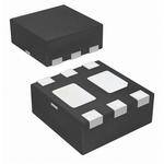
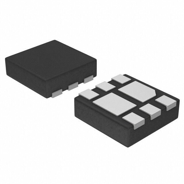
| 供应商器件封装 | 6-MicroFET(2x2) |
| 其它名称 | FDMA3023PZCT |
| 典型关闭延迟时间 | 62 ns |
| 功率-最大值 | 700mW |
| 包装 | 剪切带 (CT) |
| 单位重量 | 40 mg |
| 商标 | Fairchild Semiconductor |
| 安装类型 | 表面贴装 |
| 安装风格 | SMD/SMT |
| 封装 | Reel |
| 封装/外壳 | 6-WDFN 裸露焊盘 |
| 封装/箱体 | MicroFET-6 2x2 |
| 工厂包装数量 | 3000 |
| 晶体管极性 | P-Channel |
| 最大工作温度 | + 150 C |
| 最小工作温度 | - 55 C |
| 标准包装 | 1 |
| 漏源极电压(Vdss) | 30V |
| 电流-连续漏极(Id)(25°C时) | 2.9A |
| 系列 | FDMA3023PZ |
| 通道模式 | Enhancement |
| 配置 | Dual |


PDF Datasheet 数据手册内容提取
Is Now Part of To learn more about ON Semiconductor, please visit our website at www.onsemi.com Please note: As part of the Fairchild Semiconductor integration, some of the Fairchild orderable part numbers will need to change in order to meet ON Semiconductor’s system requirements. Since the ON Semiconductor product management systems do not have the ability to manage part nomenclature that utilizes an underscore (_), the underscore (_) in the Fairchild part numbers will be changed to a dash (-). This document may contain device numbers with an underscore (_). Please check the ON Semiconductor website to verify the updated device numbers. The most current and up-to-date ordering information can be found at www.onsemi.com. Please email any questions regarding the system integration to Fairchild_questions@onsemi.com. ON Semiconductor and the ON Semiconductor logo are trademarks of Semiconductor Components Industries, LLC dba ON Semiconductor or its subsidiaries in the United States and/or other countries. ON Semiconductor owns the rights to a number of patents, trademarks, copyrights, trade secrets, and other intellectual property. A listing of ON Semiconductor’s product/patent coverage may be accessed at www.onsemi.com/site/pdf/Patent-Marking.pdf. ON Semiconductor reserves the right to make changes without further notice to any products herein. ON Semiconductor makes no warranty, representation or guarantee regarding the suitability of its products for any particular purpose, nor does ON Semiconductor assume any liability arising out of the application or use of any product or circuit, and specifically disclaims any and all liability, including without limitation special, consequential or incidental damages. Buyer is responsible for its products and applications using ON Semiconductor products, including compliance with all laws, regulations and safety requirements or standards, regardless of any support or applications information provided by ON Semiconductor. “Typical” parameters which may be provided in ON Semiconductor data sheets and/or specifications can and do vary in different applications and actual performance may vary over time. All operating parameters, including “Typicals” must be validated for each customer application by customer’s technical experts. ON Semiconductor does not convey any license under its patent rights nor the rights of others. ON Semiconductor products are not designed, intended, or authorized for use as a critical component in life support systems or any FDA Class 3 medical devices or medical devices with a same or similar classification in a foreign jurisdiction or any devices intended for implantation in the human body. Should Buyer purchase or use ON Semiconductor products for any such unintended or unauthorized application, Buyer shall indemnify and hold ON Semiconductor and its officers, employees, subsidiaries, affiliates, and distributors harmless against all claims, costs, damages, and expenses, and reasonable attorney fees arising out of, directly or indirectly, any claim of personal injury or death associated with such unintended or unauthorized use, even if such claim alleges that ON Semiconductor was negligent regarding the design or manufacture of the part. ON Semiconductor is an Equal Opportunity/Affirmative Action Employer. This literature is subject to all applicable copyright laws and is not for resale in any manner.
F D M A 3 July 2014 0 2 FDMA3023PZ 3 P ® Z Dual P-Channel PowerTrench MOSFET D -30 V, -2.9 A, 90 mΩ u a l Features General Description P - C (cid:132) Max rDS(on) = 90 mΩ at VGS = -4.5 V, ID = -2.9 A This device is designed specifically as a single package solution h for the battery charge switch in cellular handset and other a (cid:132) Max rDS(on) = 130 mΩ at VGS = -2.5 V, ID = -2.6 A ultra-portable applications. It features two independent n P-Channel MOSFETs with low on-state resistance for minimum n (cid:132) Max rDS(on) = 170 mΩ at VGS = -1.8 V, ID = -1.7 A e conduction losses. When connected in the typical common l (cid:132) Max rDS(on) = 240 mΩ at VGS = -1.5 V, ID = -1.0 A source configuration, bi-directional current flow is possible. P o (cid:132) Low profile - 0.8 mm maximum - in the new package MicroFET w The MicroFET 2X2 package offers exceptional thermal 2x2 mm e performance for its physical size and is well suited to linear mode r (cid:132) HBM ESD protection level > 2 kV (Note 3) applications. Tr e (cid:132) RoHS Compliant n c (cid:132) Free from halogenated compounds and antimony h ® oxides M O S F PIN 1 E S1 G1 D2 T S1 1111111 6666666 D1 D1 D2 G1 2222222 5555555 G2 D2 3333333 4444444 S2 D1 G2 S2 MicroFET 2x2 MOSFET Maximum Ratings TA = 25 °C unless otherwise noted Symbol Parameter Ratings Units V Drain to Source Voltage -30 V DS V Gate to Source Voltage ±8 V GS Drain Current -Continuous (Note 1a) -2.9 I A D -Pulsed -6 Power Dissipation (Note 1a) 1.4 P W D Power Dissipation (Note 1b) 0.7 T , T Operating and Storage Junction Temperature Range -55 to +150 °C J STG Thermal Characteristics R Thermal Resistance for Single Operation, Junction to Ambient (Note 1a) 86 θJA R Thermal Resistance for Single Operation, Junction to Ambient (Note 1b) 173 θJA °C/W R Thermal Resistance for Dual Operation, Junction to Ambient (Note 1c) 69 θJA R Thermal Resistance for Dual Operation, Junction to Ambient (Note 1d) 151 θJA Package Marking and Ordering Information Device Marking Device Package Reel Size Tape Width Quantity 323 FDMA3023PZ MicroFET 2X2 7 ’’ 8 mm 3000 units ©2013 Fairchild Semiconductor Corporation 1 www.fairchildsemi.com FDMA3023PZ Rev.C1
F D Electrical Characteristics T = 25 °C unless otherwise noted M J A Symbol Parameter Test Conditions Min Typ Max Units 3 0 Off Characteristics 2 3 P BV Drain to Source Breakdown Voltage I = -250 μA, V = 0 V -30 V DSS D GS Z ΔBVDSS Breakdown Voltage Temperature I = -250 μA, referenced to 25 °C -24 mV/°C D ΔTJ Coefficient D u a IDSS Zero Gate Voltage Drain Current VDS = -24 V, VGS = 0 V -1 μA l I Gate to Source Leakage Current V = ±8 V, V = 0 V ±100 nA P GSS GS DS - C On Characteristics h a V Gate to Source Threshold Voltage V = V , I = -250 μA -0.4 -0.6 -1.0 V n GS(th) GS DS D n Δ ΔVTGJS(th) GTeamtep teor aStuoruer cCeo Tehffriceisehnotld Voltage ID = -250 μA, referenced to 25 °C 3 mV/°C el P V = -4.5 V, I = -2.9 A 71 90 o GS D w V = -2.5 V, I = -2.6 A 97 130 GS D e r Static Drain to Source On Resistance V = -1.8 V, I = -1.7 A 122 170 mΩ r DS(on) GS D T V = -1.5 V, I = -1.0 A 151 240 r GS D e V = -4.5 V, I = -2.9 A, T = 125 °C 110 140 n GS D J c gFS Forward Transconductance VDS = -5 V, ID = -2.9 A 10 S h ® Dynamic Characteristics M O C Input Capacitance 400 530 pF iss V = -15 V, V = 0 V, S Coss Output Capacitance f =D S1 MHz GS 55 70 pF F E C Reverse Transfer Capacitance 45 65 pF rss T Switching Characteristics t Turn-On Delay Time 5 10 ns d(on) tr Rise Time VDD = -15 V, ID = -1.0 A, 4 10 ns td(off) Turn-Off Delay Time VGS = -4.5 V, RGEN = 6 Ω 62 100 ns t Fall Time 18 33 ns f Q Total Gate Charge 7.9 11 nC g(TOT) V = -15 V, I = -2.9 A Q Gate to Source Charge DD D 0.9 nC gs V = -4.5 V GS Q Gate to Drain “Miller” Charge 1.9 nC gd Drain-Source Diode Characteristics I Maximum Continuous Drain-Source Diode Forward Current -1.1 A S V Source to Drain Diode Forward Voltage V = 0 V, I = -1.1 A (Note 2) -0.8 -1.2 V SD GS S t Reverse Recovery Time 18 33 ns rr I = -2.9 A, di/dt = 100 A/μs Q Reverse Recovery Charge F 6.6 13 nC rr ©2013 Fairchild Semiconductor Corporation 2 www.fairchildsemi.com FDMA3023PZ Rev.C1
F D Notes: M A 1. RθJA is determined with the device mounted on a 1 in2 oz. copper pad on a 1.5 x 1.5 in. board of FR-4 material. RθJC is guaranteed by design while RθJA is determined by the 3 user's board design. (a) RθJA = 86 °C/W when mounted on a 1 in2 pad of 2 oz copper, 1.5 " x 1.5 " x 0.062 " thick PCB. For single operation. 02 (b) RθJA = 173 °C/W when mounted on a minimum pad of 2 oz copper. For single operation. 3 (c) RθJA = 69 oC/W when mounted on a 1 in2 pad of 2 oz copper, 1.5 ” x 1.5 ” x 0.062 ” thick PCB. For dual operation. P (d) RθJA = 151 oC/W when mounted on a minimum pad of 2 oz copper. For dual operation. Z D u a amicno)2o8p u6ppn eaotCrde. d/Wo of nw2 h aeo n1z bmmo)zoi1n cu7imon3pt uepomdCe r/p.Wao dnw ohfe na2 cmp)ao6du9 on ft eo2Cd o /oWzn c aow p1ph ieenrn2. d mmc)o1oinp5upi1mne toureC.md/ W opna w dah oefn 2 oz l P-Ch a n n e l P 2. Pulse Test : Pulse Width < 300 us, Duty Cycle < 2.0% o 3. The diode connected between the gate and source serves only as protection against ESD. No gate overvoltage rating is implied. w e r T r e n c h ® M O S F E T ©2013 Fairchild Semiconductor Corporation 3 www.fairchildsemi.com FDMA3023PZ Rev.C1
F D Typical Characteristics M T = 25 °C unless otherwise noted J A 3 0 6 6 2 VGS = -4.5 V E PULSE DURATION = 80 μs 3P A) 5 VGS = -3.5 V TANC 5 DUTY CYCLE = 0.5% MAX Z D ENT ( 4 VGS = -2.5 V DRESIS 4 VGS = -1.5 V ua CURR 3 VGS = -1.8 V V = -1.5 V ALIZEE ON- 3 l P- N GS MC C , DRAID 2 PDUULTSYE C DYUCRLEA T=I O0.N5 %= 8M0A μXs NORO SOUR 2 VGS = -2.5 V VGS = -1.8 V han -I 1 N T 1 ne 00 0.5 1.0 1.5 2.0 DRAI 01 2 VGS = -33.5 V 4 V5GS = -4.5 V6 l Pow -VDS, DRAIN TO SO URCE VOLTAGE (V) -ID, DRAIN CURR ENT (A) e r T Figure 1. On Region Characteristics Figure 2. Normalized On-Resistance r e vs Drain Current and Gate Voltage n c h ® 1.6 400 M ANCE 1.4 VIDG S= =-2 -.49. 5A V )mΩ PDUULTSYE C DYUCRLEA T=I O0.N5 %= 8M0A μXs OS NORMALIZED O SOURCE ON-RESIST 11..02 rDRAIN TO ,DS(on)(CE ON-RESISTANCE 123000000 ID = -1.T45J =A 125 oC FET T 0.8 R AIN SOU TJ = 25 oC R D 0.6 0 -75 -50 -25 0 25 50 75 100 125 150 1.0 1.5 2.0 2.5 3.0 3.5 4.0 4.5 TJ, JUNCTION TEM PERATURE (oC) -VGS, GATE TO SOURCE VOLTAGE (V) Figure 3. Normalized On Resistance Figure 4. On-Resistance vs Gate to vs Junction Temperature Source Voltage 6 10 5 PDUULTSYE C DYUCRLEA T=I O0.N5 %= 8M0A μXs NT (A) VGS = 0 V E T (A) 4 VDS = -5 V URR 1 URREN 3 RAIN C 0.1 TJ = 125 oC AIN C 2 TJ = 125 oC RSE D TJ = 25 oC R E -I, DD 1 TJ = 25 oC TJ = -55 oC -I, REVS0.01 TJ = -55 oC 0 0.001 0.5 1.0 1.5 2.0 0.2 0.4 0.6 0.8 1.0 1.2 -VGS, GATE TO SO URCE VOLTAGE (V) -VSD, BODY DIODE FO RWARD VOLTAGE (V) Figure 5. Transfer Characteristics Figure 6. Source to Drain Diode Forward Voltage vs Source Current ©2013 Fairchild Semiconductor Corporation 4 www.fairchildsemi.com FDMA3023PZ Rev.C1
F D Typical Characteristics T = 25 °C unless otherwise noted M J A 3 0 5 1000 2 E (V) ID = -2.9 A 3P G 4 Z A T D URCE VOL 3 VDD = -10 V VDD = -2V0D VD = -15 V ANCE (pF) 100 Ciss ual P O SO 2 ACIT Coss -Ch -V, GATE TGS 01 CAP 10 fV =G S1 =M 0H Vz Crss annel P 0 2 4 6 8 10 0.1 1 10 30 o Qg, GATE CHARGE (nC) -VDS, DRAIN TO SOU RCE VOLTAGE (V) we r T Figure 7. Gate Charge Characteristics Figure 8. Capacitance vs Drain r e to Source Voltage n c h ® 10 10-2 THIS AREA IS M RENT (A) 1100--43 VGS = 0 V NT (A) 1 LIMITED BY rDS(on) 1 ms OSFE UR RE 10 ms T GE C 10-5 TJ = 125 oC CUR 100 ms A N , GATE LEAKg 111000---876 TJ = 25 oC -I, DRAID 0.1 RSTTJAIθN J ==AG M2=L5 AE1 Xo 7PC3 RU oALCST/WEED 11D 0Cs s -I 0.01 10-9 0.01 0.1 1 10 100 200 0 3 6 9 12 15 -VDS, DRAIN to SOU RCE VOLTAGE (V) -VGS, GATE TO SOURCE VOLTAGE (V) Figure 9. Gate Leakage vs Gate to Source Voltage Figure 10. Forward Bias Safe Operating Area 200 V = -4.5 V W)100 GS SINGLE PULSE R ( RθJA = 173 oC/W WE TA = 25 oC O P T N E SI 10 N A R T K A E P , )PK 1 P( 0.5 10-3 10-2 10-1 1 10 1000 t, PULSE WIDTH (sec) Figure 11. Single Pulse Maximum Power Dissipation ©2013 Fairchild Semiconductor Corporation 5 www.fairchildsemi.com FDMA3023PZ Rev.C1
F D Typical Characteristics T = 25 °C unless otherwise noted M J A 3 0 2 2 3 P DUTY CYCLE-DESCENDING ORDER 1 Z D AL D = 0.5 u RMALIZED THERM IMPEDANCE,ZJAθ 0.1 00000.....21000521 PDM t1t2 al P-Chan NO NOTES: n SINGLE PULSE DUTY FACTOR: D = t1/t2 e 0.01 RθJA = 173 oC/W PEAK TJ = PDM x ZθJA x RθJA + TA l P 0.005 o 10-3 10-2 10-1 1 10 100 1000 w t, RECTANGULAR PULSE DURATION (sec) e r T Figure 12. Junction-to-Ambient Transient Thermal Response Curve r e n c h ® M O S F E T ©2013 Fairchild Semiconductor Corporation 6 www.fairchildsemi.com FDMA3023PZ Rev.C1
F D Dimensional Outline and Pad Layout M A 3 0 2 3 P Z D u a l P - C h a n n e l P o w e r T r e n c h ® M O S F E T Package drawings are provided as a service to customers considering Fairchild components. Drawings may change in any manner without notice. Please note the revision and/or date on the drawing and contact a Fairchild Semiconductor representative to verify or obtain the most recent revision. Package specifications do not expand the terms of Fairchild’s worldwide terms and conditions, specif- ically the warranty therein, which covers Fairchild products. Always visit Fairchild Semiconductor’s online packaging area for the most recent package drawings: http://www.fairchildsemi.com/package/packageDetails.html?id=PN_MLDEB-X06 ©2013 Fairchild Semiconductor Corporation www.fairchildsemi.com FDMA3023PZ Rev.C1
F D M A 3 0 2 3 P Z TRADEMARKS D The following includes registered and unregistered trademarks and service marks, owned by Fairchild Semiconductor and/or its global subsidiaries, and is not u intended to be an exhaustive list of all such trademarks. a AAXcc-uCPAoPw®e*r™ FFR-PFFEST™® ® ®* l P BitSiC™ Global Power ResourceSM PowtmerTrench® TinyBoost® -C Build it Now™ GreenBridge™ PowerXS™ TinyBuck® h CorePLUS™ Green FPS™ Programmable Active Droop™ a CCoRrOePSOSVWOELRT™™ GGrmeaexn™ FPS™ e-Series™ QQSFE™T® TTiinnyyCLoaglcic™® nn CTL™ GTO™ Quiet Series™ TINYOPTO™ e TinyPower™ l CDuErUreXnPt ETEraDn®sfer Logic™ IInStOelPliMLAANXA™R™ Rapid™Configure™ TTiinnyyWPWireM™™ Po DEcuoaSl CPAooRl™K® Manadr kBinegtt eSrm™all Speakers Sound Louder Saving our world, 1mW/W/kW at a time™ TranSiC™ w TriFault Detect™ e EEfSfiBceCn™tMax™ MMeICgRaBOuCcOk™UPLER™ SSimgnaartlMWaisxe™™ TRUECURRENT®* rT ® MicroFET™ SMART START™ μSerDes™ re MicroPak™ Solutions for Your Success™ n Fairchild® MicroPak2™ SPM® c Fairchild Semiconductor® MillerDrive™ STEALTH™ UHC® h FACT Quiet Series™ MotionMax™ SuperFET® Ultra FRFET™ ® FACT® mWSaver® SuperSOT™-3 UniFET™ M FFaAsStTvC®ore™ OOpPtToOHLiTO™GIC® SSuuppeerrSSOOTT™™--68 VViCsXua™lMax™ O FETBench™ OPTOPLANAR® SupreMOS® VoltagePlus™ S FPS™ SyncFET™ XS™ F Sync-Lock™ 仙童™ E T *Trademarks of System General Corporation, used under license by Fairchild Semiconductor. DISCLAIMER FAIRCHILD SEMICONDUCTOR RESERVES THE RIGHT TO MAKE CHANGES WITHOUT FURTHER NOTICE TO ANY PRODUCTS HEREIN TO IMPROVE RELIABILITY, FUNCTION, OR DESIGN. FAIRCHILD DOES NOT ASSUME ANY LIABILITY ARISING OUT OF THE APPLICATION OR USE OF ANY PRODUCT OR CIRCUIT DESCRIBED HEREIN; NEITHER DOES IT CONVEY ANY LICENSE UNDER ITS PATENT RIGHTS, NOR THE RIGHTS OF OTHERS. THESE SPECIFICATIONS DO NOT EXPAND THE TERMS OF FAIRCHILD’S WORLDWIDE TERMS AND CONDITIONS, SPECIFICALLY THE WARRANTY THEREIN, WHICH COVERS THESE PRODUCTS. LIFE SUPPORT POLICY FAIRCHILD’S PRODUCTS ARE NOT AUTHORIZED FOR USE AS CRITICAL COMPONENTS IN LIFE SUPPORT DEVICES OR SYSTEMS WITHOUT THE EXPRESS WRITTEN APPROVAL OF FAIRCHILD SEMICONDUCTOR CORPORATION. As used here in: 1. Life support devices or systems are devices or systems which, (a) are 2. A critical component in any component of a life support, device, or intended for surgical implant into the body or (b) support or sustain life, system whose failure to perform can be reasonably expected to cause and (c) whose failure to perform when properly used in accordance with the failure of the life support device or system, or to affect its safety or instructions for use provided in the labeling, can be reasonably effectiveness. expected to result in a significant injury of the user. ANTI-COUNTERFEITING POLICY Fairchild Semiconductor Corporation’s Anti-Counterfeiting Policy. Fairchild’s Anti-Counterfeiting Policy is also stated on our external website, www.Fairchildsemi.com, under Sales Support. Counterfeiting of semiconductor parts is a growing problem in the industry. All manufactures of semiconductor products are experiencing counterfeiting of their parts. Customers who inadvertently purchase counterfeit parts experience many problems such as loss of brand reputation, substandard performance, failed application, and increased cost of production and manufacturing delays. Fairchild is taking strong measures to protect ourselves and our customers from the proliferation of counterfeit parts. Fairchild strongly encourages customers to purchase Fairchild parts either directly from Fairchild or from Authorized Fairchild Distributors who are listed by country on our web page cited above. Products customers buy either from Fairchild directly or from Authorized Fairchild Distributors are genuine parts, have full traceability, meet Fairchild’s quality standards for handing and storage and provide access to Fairchild’s full range of up-to-date technical and product information. Fairchild and our Authorized Distributors will stand behind all warranties and will appropriately address and warranty issues that may arise. Fairchild will not provide any warranty coverage or other assistance for parts bought from Unauthorized Sources. Fairchild is committed to combat this global problem and encourage our customers to do their part in stopping this practice by buying direct or from authorized distributors. PRODUCT STATUS DEFINITIONS Definition of Terms Datasheet Identification Product Status Definition Datasheet contains the design specifications for product development. Specifications Advance Information Formative / In Design may change in any manner without notice. Datasheet contains preliminary data; supplementary data will be published at a later Preliminary First Production date. Fairchild Semiconductor reserves the right to make changes at any time without notice to improve design. Datasheet contains final specifications. Fairchild Semiconductor reserves the right to No Identification Needed Full Production make changes at any time without notice to improve the design. Datasheet contains specifications on a product that is discontinued by Fairchild Obsolete Not In Production Semiconductor. The datasheet is for reference information only. Rev. I68 ©2013 Fairchild Semiconductor Corporation www.fairchildsemi.com FDMA3023PZ Rev.C1
ON Semiconductor and are trademarks of Semiconductor Components Industries, LLC dba ON Semiconductor or its subsidiaries in the United States and/or other countries. ON Semiconductor owns the rights to a number of patents, trademarks, copyrights, trade secrets, and other intellectual property. A listing of ON Semiconductor’s product/patent coverage may be accessed at www.onsemi.com/site/pdf/Patent−Marking.pdf. ON Semiconductor reserves the right to make changes without further notice to any products herein. ON Semiconductor makes no warranty, representation or guarantee regarding the suitability of its products for any particular purpose, nor does ON Semiconductor assume any liability arising out of the application or use of any product or circuit, and specifically disclaims any and all liability, including without limitation special, consequential or incidental damages. Buyer is responsible for its products and applications using ON Semiconductor products, including compliance with all laws, regulations and safety requirements or standards, regardless of any support or applications information provided by ON Semiconductor. “Typical” parameters which may be provided in ON Semiconductor data sheets and/or specifications can and do vary in different applications and actual performance may vary over time. All operating parameters, including “Typicals” must be validated for each customer application by customer’s technical experts. ON Semiconductor does not convey any license under its patent rights nor the rights of others. ON Semiconductor products are not designed, intended, or authorized for use as a critical component in life support systems or any FDA Class 3 medical devices or medical devices with a same or similar classification in a foreign jurisdiction or any devices intended for implantation in the human body. Should Buyer purchase or use ON Semiconductor products for any such unintended or unauthorized application, Buyer shall indemnify and hold ON Semiconductor and its officers, employees, subsidiaries, affiliates, and distributors harmless against all claims, costs, damages, and expenses, and reasonable attorney fees arising out of, directly or indirectly, any claim of personal injury or death associated with such unintended or unauthorized use, even if such claim alleges that ON Semiconductor was negligent regarding the design or manufacture of the part. ON Semiconductor is an Equal Opportunity/Affirmative Action Employer. This literature is subject to all applicable copyright laws and is not for resale in any manner. PUBLICATION ORDERING INFORMATION LITERATURE FULFILLMENT: N. American Technical Support: 800−282−9855 Toll Free ON Semiconductor Website: www.onsemi.com Literature Distribution Center for ON Semiconductor USA/Canada 19521 E. 32nd Pkwy, Aurora, Colorado 80011 USA Europe, Middle East and Africa Technical Support: Order Literature: http://www.onsemi.com/orderlit Phone: 303−675−2175 or 800−344−3860 Toll Free USA/Canada Phone: 421 33 790 2910 Fax: 303−675−2176 or 800−344−3867 Toll Free USA/Canada Japan Customer Focus Center For additional information, please contact your local Email: orderlit@onsemi.com Phone: 81−3−5817−1050 Sales Representative © Semiconductor Components Industries, LLC www.onsemi.com www.onsemi.com 1
Mouser Electronics Authorized Distributor Click to View Pricing, Inventory, Delivery & Lifecycle Information: O N Semiconductor: FDMA3023PZ