ICGOO在线商城 > 分立半导体产品 > 晶体管 - FET,MOSFET - 单 > FDH038AN08A1

 Datasheet下载
- 型号: FDH038AN08A1
- 制造商: Fairchild Semiconductor
- 库位|库存: xxxx|xxxx
- 要求:
| 数量阶梯 | 香港交货 | 国内含税 |
| +xxxx | $xxxx | ¥xxxx |
查看当月历史价格
查看今年历史价格
FDH038AN08A1产品简介:
ICGOO电子元器件商城为您提供FDH038AN08A1由Fairchild Semiconductor设计生产,在icgoo商城现货销售,并且可以通过原厂、代理商等渠道进行代购。 FDH038AN08A1价格参考。Fairchild SemiconductorFDH038AN08A1封装/规格:晶体管 - FET,MOSFET - 单, 通孔 N 沟道 75V 22A(Ta),80A(Tc) 450W(Tc) TO-247。您可以下载FDH038AN08A1参考资料、Datasheet数据手册功能说明书,资料中有FDH038AN08A1 详细功能的应用电路图电压和使用方法及教程。
FDH038AN08A1 是一款由 ON Semiconductor(安森美半导体)生产的 N 沟道增强型 MOSFET(金属氧化物半导体场效应晶体管)。其主要应用场景包括但不限于以下领域:

 1. 电源管理
   - DC-DC 转换器:用于开关电源中的高频开关,实现高效的电压转换。
   - 负载开关:在便携式设备中控制电路的通断,降低功耗。
   - 降压/升压电路:适用于各种需要调节输出电压的场景。

 2. 电机驱动
   - 小型电机控制:如风扇、泵或家用电器中的电机驱动,提供高效开关和低导通电阻。
   - H 桥电路:用于双向电机控制,支持正转和反转功能。

 3. 电池管理系统 (BMS)
   - 电池保护:通过快速开关特性防止过流、短路等异常情况。
   - 充电电路:用于锂离子电池或其他类型电池的充电管理。

 4. 汽车电子
   - 车载电子设备:如车窗升降器、座椅调节、雨刷控制系统等。
   - LED 照明驱动:为汽车内外部 LED 灯提供稳定电流。

 5. 消费类电子产品
   - 适配器与充电器:用于 USB 充电器、快充设备等,提供高效率和低热损耗。
   - 音频放大器:作为开关元件,优化功率传输并减少失真。

 6. 工业自动化
   - 继电器替代:利用其固态特性,取代传统机械继电器以提高可靠性。
   - 传感器接口:为工业传感器提供信号调理和功率控制。

 7. 通信设备
   - 基站电源:在通信基础设施中用作高效功率转换元件。
   - 信号调节:在射频前端模块中起到开关或限流作用。

 特性优势:
- 低导通电阻 (Rds(on)):减少传导损耗,提升系统效率。
- 高开关速度:适合高频应用,降低开关损耗。
- 优异的热性能:确保长时间稳定运行,适用于紧凑设计。

总之,FDH038AN08A1 凭借其高性能参数,广泛应用于需要高效功率转换和低损耗的各类电子系统中。
| 参数 | 数值 |
| 产品目录 | |
| ChannelMode | Enhancement |
| 描述 | MOSFET N-CH 75V 80A TO-247MOSFET N-Ch PowerTrench |
| 产品分类 | FET - 单分离式半导体 |
| FET功能 | 标准 |
| FET类型 | MOSFET N 通道,金属氧化物 |
| Id-ContinuousDrainCurrent | 80 A |
| Id-连续漏极电流 | 80 A |
| 品牌 | Fairchild Semiconductor |
| 产品手册 | |
| 产品图片 |
|
| rohs | 符合RoHS无铅 / 符合限制有害物质指令(RoHS)规范要求 |
| 产品系列 | 晶体管,MOSFET,Fairchild Semiconductor FDH038AN08A1PowerTrench® |
| 数据手册 | |
| 产品型号 | FDH038AN08A1 |
| PCN设计/规格 | |
| Pd-PowerDissipation | 450 W |
| Pd-功率耗散 | 450 W |
| RdsOn-Drain-SourceResistance | 3.5 mOhms |
| RdsOn-漏源导通电阻 | 3.5 mOhms |
| Vds-Drain-SourceBreakdownVoltage | 75 V |
| Vds-漏源极击穿电压 | 75 V |
| Vgs-Gate-SourceBreakdownVoltage | +/- 20 V |
| Vgs-栅源极击穿电压 | 20 V |
| 上升时间 | 141 ns |
| 下降时间 | 126 ns |
| 不同Id时的Vgs(th)(最大值) | 4V @ 250µA |
| 不同Vds时的输入电容(Ciss) | 8665pF @ 25V |
| 不同Vgs时的栅极电荷(Qg) | 160nC @ 10V |
| 不同 Id、Vgs时的 RdsOn(最大值) | 3.8 毫欧 @ 80A,10V |
| 产品培训模块 | http://www.digikey.cn/PTM/IndividualPTM.page?site=cn&lang=zhs&ptm=356 |
| 产品种类 | MOSFET |
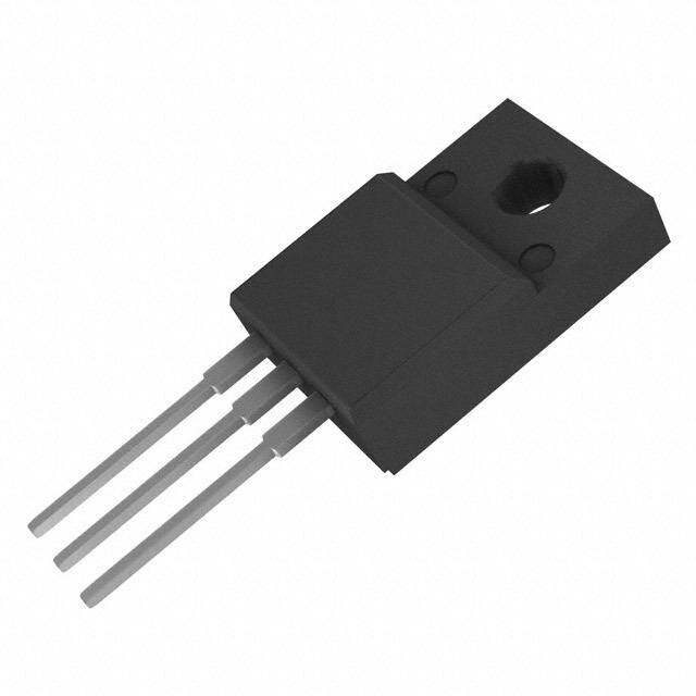
| 供应商器件封装 | TO-247 |
| 典型关闭延迟时间 | 232 ns |
| 功率-最大值 | 450W |
| 包装 | 管件 |
| 单位重量 | 6.390 g |
| 商标 | Fairchild Semiconductor |
| 安装类型 | 通孔 |
| 安装风格 | Through Hole |
| 封装 | Tube |
| 封装/外壳 | TO-247-3 |
| 封装/箱体 | TO-247-3 |
| 工厂包装数量 | 30 |
| 晶体管极性 | N-Channel |
| 最大工作温度 | + 175 C |
| 最小工作温度 | - 55 C |
| 标准包装 | 30 |
| 漏源极电压(Vdss) | 75V |
| 电流-连续漏极(Id)(25°C时) | 22A (Ta), 80A (Tc) |
| 系列 | FDH038AN08A1 |
| 通道模式 | Enhancement |
| 配置 | Single |
| 零件号别名 | FDH038AN08A1_NL |


PDF Datasheet 数据手册内容提取
Is Now Part of To learn more about ON Semiconductor, please visit our website at www.onsemi.com Please note: As part of the Fairchild Semiconductor integration, some of the Fairchild orderable part numbers will need to change in order to meet ON Semiconductor’s system requirements. Since the ON Semiconductor product management systems do not have the ability to manage part nomenclature that utilizes an underscore (_), the underscore (_) in the Fairchild part numbers will be changed to a dash (-). This document may contain device numbers with an underscore (_). Please check the ON Semiconductor website to verify the updated device numbers. The most current and up-to-date ordering information can be found at www.onsemi.com. Please email any questions regarding the system integration to Fairchild_questions@onsemi.com. ON Semiconductor and the ON Semiconductor logo are trademarks of Semiconductor Components Industries, LLC dba ON Semiconductor or its subsidiaries in the United States and/or other countries. ON Semiconductor owns the rights to a number of patents, trademarks, copyrights, trade secrets, and other intellectual property. A listing of ON Semiconductor’s product/patent coverage may be accessed at www.onsemi.com/site/pdf/Patent-Marking.pdf. ON Semiconductor reserves the right to make changes without further notice to any products herein. ON Semiconductor makes no warranty, representation or guarantee regarding the suitability of its products for any particular purpose, nor does ON Semiconductor assume any liability arising out of the application or use of any product or circuit, and specifically disclaims any and all liability, including without limitation special, consequential or incidental damages. Buyer is responsible for its products and applications using ON Semiconductor products, including compliance with all laws, regulations and safety requirements or standards, regardless of any support or applications information provided by ON Semiconductor. “Typical” parameters which may be provided in ON Semiconductor data sheets and/or specifications can and do vary in different applications and actual performance may vary over time. All operating parameters, including “Typicals” must be validated for each customer application by customer’s technical experts. ON Semiconductor does not convey any license under its patent rights nor the rights of others. ON Semiconductor products are not designed, intended, or authorized for use as a critical component in life support systems or any FDA Class 3 medical devices or medical devices with a same or similar classification in a foreign jurisdiction or any devices intended for implantation in the human body. Should Buyer purchase or use ON Semiconductor products for any such unintended or unauthorized application, Buyer shall indemnify and hold ON Semiconductor and its officers, employees, subsidiaries, affiliates, and distributors harmless against all claims, costs, damages, and expenses, and reasonable attorney fees arising out of, directly or indirectly, any claim of personal injury or death associated with such unintended or unauthorized use, even if such claim alleges that ON Semiconductor was negligent regarding the design or manufacture of the part. ON Semiconductor is an Equal Opportunity/Affirmative Action Employer. This literature is subject to all applicable copyright laws and is not for resale in any manner.
F D H 0 October 2013 3 8 A FDH038AN08A1 N 0 ® 8 N-Channel PowerTrench MOSFET A 1 75 V, 80 A, 3.8 mΩ — N Features Applications - C • RDS(ON) = 3.5 mΩ (Typ.), VGS = 10 V, ID = 80 A • Synchronous Rectification for ATX / Server / Telecom PSU ha n • Qg(tot) = 125 nC (Typ.), VGS = 10 V • Battery Protection Circuit n e • Low Miller Charge • Motor Drives and Uninterruptible Power Supplies l P • Low Qrr Body Diode o w • UIS Capability (Single Pulse and Repetitive Pulse) e r T Formerly developmental type 82690 r e n c D h ® M O S F E G T G D TO-247 S S MOSFET Maximum Ratings TC = 25°C unless otherwise noted Symbol Parameterr FDH038AN08A1 Unit V Drain to Source Voltage 75 V DSS V Gate to Source Voltage ±20 V GS Drain Current Continuous (T < 158oC, V = 10V) 80 A I C GS D Continuous (TA = 25oC, VGS = 10V, with RθJA = 30oC/W) 22 A Pulsed Figure 4 A E Single Pulse Avalanche Energy (Note 1) 1.17 J AS Power dissipation 450 W P D Derate above 25oC 3.0 W/oC T , T Operating and Storage Temperature -55 to 175 oC J STG Thermal Characteristics RθJC Thermal Resistance Junction to Case, Max. TO-247 0.33 oC/W RθJA Thermal Resistance Junction to Ambient, Max. TO-247 30 oC/W ©2003 Fairchild Semiconductor Corporation 1 www.fairchildsemi.com FDH038AN08A1 Rev. C2
F D Package Marking and Ordering Information H 0 Device Marking Device Package Reel Size Tape Width Quantity 3 FDH038AN08A1 FDH038AN08A1 TO-247 Tube N/A 30 units 8 A N Electrical Characteristics T = 25°C unless otherwise noted 0 C 8 A Symbol Parameter Test Conditions Min Typ Max Unit 1 Off Characteristics — B Drain to Source Breakdown Voltage I = 250µA, V = 0V 75 - - V N VDSS D GS - V = 60V - - 1 C IDSS Zero Gate Voltage Drain Current VDS = 0V T = 150oC - - 250 µA h GS C a I Gate to Source Leakage Current V = ±20V - - ±100 nA n GSS GS n e On Characteristics l P VGS(TH) Gate to Source Threshold Voltage VGS = VDS, ID = 250µA 2 - 4 V o w I = 80A, V = 10V - 0.0035 0.0038 D GS e r Drain to Source On Resistance ID = 40A, VGS = 6V - 0.0047 0.0071 Ω rT DS(ON) I = 80A, V = 10V, r D GS - 0.0074 0.008 e TJ = 175oC n c h Dynamic Characteristics ® C Input Capacitance - 8665 - pF M ISS C Output Capacitance VDS = 25V, VGS = 0V, - 1320 - pF O OSS f = 1MHz S CRSS Reverse Transfer Capacitance - 340 - pF F E Q Total Gate Charge at 10V V = 0V to 10V 125 160 nC g(TOT) GS T Qg(TH) Threshold Gate Charge VGS = 0V to 2V VDD = 40V - 17 22 nC Q Gate to Source Gate Charge I = 80A - 57 - nC gs D Qgs2 Gate Charge Threshold to Plateau Ig = 1.0mA - 42 - nC Q Gate to Drain “Miller” Charge - 30 - nC gd Switching Characteristics (V = 10V) GS t Turn-On Time - - 345 ns ON t Turn-On Delay Time - 88 - ns d(ON) tr Rise Time VDD = 40V, ID = 80A - 141 - ns td(OFF) Turn-Off Delay Time VGS = 10V, RGS = 2.4Ω - 232 - ns t Fall Time - 126 - ns f t Turn-Off Time - - 530 ns OFF Drain-Source Diode Characteristics I = 80A - - 1.25 V V Source to Drain Diode Voltage SD SD I = 40A - - 1.0 V SD t Reverse Recovery Time I = 75A, dI /dt = 100A/µs - - 50 ns rr SD SD Q Reverse Recovered Charge I = 75A, dI /dt = 100A/µs - - 65 nC RR SD SD Notes: 1: Starting TJ = 25°C, L = 0.65mH, IAS = 60A. ©2003 Fairchild Semiconductor Corporation 2 www.fairchildsemi.com FDH038AN08A1 Rev. C2
F D Typical Characteristics TC = 25°C unless otherwise noted H 0 1.2 280 38 CURRENT LIMITED A R 1.0 240 BY PACKAGE N E LTIPLI 0.8 T (A) 200 08A U N M E 1 ON 0.6 URR 160 — TI C SIPA AIN 120 N S 0.4 R - ER DI I, DD 80 Ch W 0.2 a O 40 n P VGS = 10V n 0 0 e 0 25 50 75 100 125 150 175 l 25 50 75 100 125 150 175 P TC, CASE TEMPERATURE (oC) TC, CASE TEMPERATURE (oC) ow e Figure 1. Normalized Power Dissipation vs Figure 2. Maximum Continuous Drain Current vs r Ambient Temperature Case Temperature T r e n c 2 RθJA=30oC/W h ® 1 DUTY CYCLE - DESCENDING ORDER 0.5 M NORMALIZEDAL IMPEDANCE 0.1 00000.....21000512 PDM OSFET Z, θJCHERM t1 T t2 NOTES: DUTY FACTOR: D = t1/t2 SINGLE PULSE PEAK TJ = PDM x ZθJC x RθJC + TC 0.01 10-5 10-4 10-3 10-2 10-1 100 101 t, RECTANGULAR PULSE DURATION (s) Figure 3. Normalized Maximum Transient Thermal Impedance 3000 TC = 25oC FOR TEMPERATURES TRANSCONDUCTANCE MAY LIMIT CURRENT ABOVE 25oC DERATE PEAK IN THIS REGION CURRENT AS FOLLOWS: 1000 A) T ( I = I25 175 - TC EN VGS = 10V 150 R R U C K A E P , M D I 100 50 10-5 10-4 10-3 10-2 10-1 100 101 t, PULSE WIDTH (s) Figure 4. Peak Current Capability ©2003 Fairchild Semiconductor Corporation 3 www.fairchildsemi.com FDH038AN08A1 Rev. C2
F D Typical Characteristics TC = 25°C unless otherwise noted H 0 3 2000 500 10µs If R = 0 8 1000 tAV = (L)(IAS)/(1.3*RATED BVDSS - VDD) A ENT (A)100 11m00sµs URRENT (A)100 ItfA RV =≠ (0L/R)ln[(IAS*R)/(1.3*RATED BVDSSTSA -R VTDIND)G + T1]J = 25oC N08A1 R C I, DRAIN CURD 110 OLPIMEIARTRAETEDIA OB NMY AIrNDY S TB(OHENIS) DC 10ms , AVALANCHE AS 10 STARTING TJ = 150oC — N-Cha SINGLE PULSE I n TJ = MAX RATED n TC = 25oC 1 e 0.1 l 0.1 1 10 100 0.01 0.1 1 10 100 P VDS, DRAIN TO SOURCE VOLTAGE (V) tAV, TIME IN AVALANCHE (ms) o w Figure 5. Forward Bias Safe Operating Area NOTE: Refer to Fairchild Application Notes AN7514 and AN7515 e r Figure 6. Unclamped Inductive Switching T Capability re n c h 160 160 PULSE DURATION = 80ms ® DUTY CYCLE = 0.5% MAX VGS = 10V VGS = 7V M VDD = 15V O A)120 A) 120 S RRENT ( TJ = 175oC RRENT ( VGS = 6V VGS = 5V FET CU 80 CU 80 N N DRAI TJ = 25oC TJ = -55oC DRAI I, D 40 I, D 40 TC = 25oC PULSE DURATION = 80µs DUTY CYCLE = 0.5% MAX 0 0 3.0 3.5 4.0 4.5 5.0 5.5 6.0 0 0.5 1.0 1.5 VGS, GATE TO SOURCE VOLTAGE (V) VDS, DRAIN TO SOURCE VOLTAGE (V) Figure 7. Transfer Characteristics Figure 8. Saturation Characteristics Ω) 6 2.5 PULSE DURATION = 80µs m TANCE( 5 VGS = 6V URCE 2.0 DUTY CYCLE = 0.5% MAX S O N RESI N TO STANCE CE O 4 VGS = 10V DRAIESIS1.5 OUR ZED ON R TO S 3 MALI 1.0 N R DRAI PDUULTSYE C DYUCRLEA T=I O0.N5 %= 8M0AµsX NO VGS = 10V, ID = 80A 2 0.5 0 20 40 60 80 -80 -40 0 40 80 120 160 200 ID, DRAIN CURRENT (A) TJ, JUNCTION TEMPERATURE (oC) Figure 9. Drain to Source On Resistance vs Drain Figure 10. Normalized Drain to Source On Current Resistance vs Junction Temperature ©2003 Fairchild Semiconductor Corporation 4 www.fairchildsemi.com FDH038AN08A1 Rev. C2
F D Typical Characteristics TC = 25°C unless otherwise noted H 0 3 1.4 1.2 VGS = VDS, ID = 250µA ID = 250µA 8A 1.2 CE N URE 0 NORMALIZED GATEHRESHOLD VOLTAGE001...680 ALIZED DRAIN TO SOREAKDOWN VOLTAG11..01 8A1 — N-C T MB h 0.4 OR a N n n 0.2 0.9 e l -80 -40 0 40 80 120 160 200 -80 -40 0 40 80 120 160 200 P TJ, JUNCTION TEMPERATURE (oC) TJ, JUNCTION TEMPERATURE (oC) o w Figure 11. Normalized Gate Threshold Voltage vs Figure 12. Normalized Drain to Source e r Junction Temperature Breakdown Voltage vs Junction Temperature T r e n 20000 10 c CISS = CGS + CGD VDD = 40V h® 10000 V) E ( 8 M NCE (pF) COSS ≅ CDS + CGD CE VOLTAG 6 OSFE APACITA 1000 CRSS = CGD O SOUR 4 T C, C ATE T WAVEFORMS IN , GGS 2 DESCIDE =N 8D0INAG ORDER: VGS = 0V, f = 1MHz V ID = 40A 100 0 0.1 1 10 75 0 25 50 75 100 125 VDS, DRAIN TO SOURCE VOLTAGE (V) Qg, GATE CHARGE (nC) Figure 13. Capacitance vs Drain to Source Figure 14. Gate Charge Waveforms for Constant Voltage Gate Currents ©2003 Fairchild Semiconductor Corporation 5 www.fairchildsemi.com FDH038AN08A1 Rev. C2
F D Test Circuits and Waveforms H 0 3 8 A VDS N BVDSS 0 8 L tP A VDS 1 VRAERQYU ItRP ETDO POEBATKA IINAS RG +VDD IAS VDD — N VGS - -C DUT h a tP n 0V IAS n 0.01Ω 0 el P tAV o w e Figure 15. Unclamped Energy Test Circuit Figure 16. Unclamped Energy Waveforms r T r e n c VDS h ® VDD Qg(TOT) M L VDS O VGS VGS = 10V S VGS + FE VDD Qgs2 T - DUT Ig(REF) VGS = 2V 0 Qg(TH) Qgs Qgd Ig(REF) 0 Figure 17. Gate Charge Test Circuit Figure 18. Gate Charge Waveforms VDS tON tOFF td(ON) td(OFF) RL tr tf VDS 90% 90% + VGS VDD 10% 10% - 0 DUT 90% RGS VGS 50% 50% PULSE WIDTH VGS 10% 0 Figure 19. Switching Time Test Circuit Figure 20. Switching Time Waveforms ©2003 Fairchild Semiconductor Corporation 6 www.fairchildsemi.com FDH038AN08A1 Rev. C2
F PSPICE Electrical Model D H .SUBCKT FDH038AN08A1 2 1 3 ; rev January 2003 0 CA 12 8 1.0e-9 3 8 Cb 15 14 3.1e-9 A LDRAIN Cin 6 8 8.22e-9 DPLCAP 5 DRAIN N 2 0 Dbody 7 5 DbodyMOD 10 8 Dbreak 5 11 DbreakMOD RSLC1 RLDRAIN A Dplcap 10 5 DplcapMOD RSLC2 +51 DBREAK 1 5 — Ebreak 11 7 17 18 84.9 51 ESLC 11 Eds 14 8 5 8 1 -50 + N EEgsgs 163 1 80 66 88 11 ESG -68 RDRAIN EBREAK 1178 DBODY -Ch Evthres 6 21 19 8 1 + EVTHRES 16 - a Evtemp 20 6 18 22 1 LGATE EVTEMP + 189 - 21 MWEAK nn It 8 17 1 GA1TE 9RGATE20+ 1282 - 6 MMED el Lgate 1 9 4.81e-9 RLGATE MSTRO Po LSOURCE LLdsorauirnc e2 35 71 .40.e6-39e-9 CIN 8 7 SOU3RCE we RSOURCE r RLgate 1 9 48.1 RLSOURCE T RRLLdsorauirnc e2 35 71 046.3 12S1A13 14S2A 15 17 RBREAK 18 ren 8 13 c Mmed 16 6 8 8 MmedMOD S1B S2B RVTEMP h® MMswteroa k1 61 66 281 8 8 M 8s MtrowMeOakDM OD CA 13++ CB+ 14 IT -19 M Rbreak 17 18 RbreakMOD 1 EGS 68 EDS 58 + VBAT OS Rdrain 50 16 RdrainMOD 2.0e-4 -- - 8 F 22 E Rgate 9 20 20 RVTHRES T RSLC1 5 51 RSLCMOD 1.0e-6 RSLC2 5 50 1e3 Rsource 8 7 RsourceMOD 2.6e-3 Rvthres 22 8 RvthresMOD 1 Rvtemp 18 19 RvtempMOD 1 S1a 6 12 13 8 S1AMOD S1b 13 12 13 8 S1BMOD S2a 6 15 14 13 S2AMOD S2b 13 15 14 13 S2BMOD Vbat 22 19 DC 1 ESLC 51 50 VALUE={(V(5,51)/ABS(V(5,51)))*(PWR(V(5,51)/(1e-6*300),10))} .MODEL DbodyMOD D (IS=2.4E-11 N=1.02 RS=1.65e-3 TRS1=3.2e-3 TRS2=2.0e-7 + CJO=6.0e-9 M=5.6e-1 TT=2.38e-8 XTI=3.9) .MODEL DbreakMOD D (RS=1.5e-1 TRS1=1.0e-3 TRS2=-8.9e-6) .MODEL DplcapMOD D (CJO=1.5e-9 IS=1.0e-30 N=10 M=0.47) .MODEL MmedMOD NMOS (VTO=3.2 KP=1.5 IS=1.0e-30 N=10 TOX=1 L=1u W=1u RG=20) .MODEL MstroMOD NMOS (VTO=3.95 KP=235 IS=1.0e-30 N=10 TOX=1 L=1u W=1u) .MODEL MweakMOD NMOS (VTO=2.73 KP=0.02 IS=1e-30 N=10 TOX=1 L=1u W=1u RG=200 RS=.01) .MODEL RbreakMOD RES (TC1=1.05e-3 TC2=-9.0e-7) .MODEL RdrainMOD RES (TC1=1.8e-2 TC2=2.2e-4) .MODEL RSLCMOD RES (TC1=2.0e-3 TC2=1.0e-5) .MODEL RsourceMOD RES (TC1=5.0e-3 TC2=1.0e-6) .MODEL RvthresMOD RES (TC1=-4.2e-3 TC2=-1.8e-5) .MODEL RvtempMOD RES (TC1=-4.5e-3 TC2=2.0e-6) .MODEL S1AMOD VSWITCH (RON=1e-5 ROFF=0.1 VON=-4 VOFF=-1.5) .MODEL S1BMOD VSWITCH (RON=1e-5 ROFF=0.1 VON=-1.5 VOFF=-4) .MODEL S2AMOD VSWITCH (RON=1e-5 ROFF=0.1 VON=-0.5 VOFF=0.5) .MODEL S2BMOD VSWITCH (RON=1e-5 ROFF=0.1 VON=0.5 VOFF=-0.5) .ENDS Note: For further discussion of the PSPICE model, consult A New PSPICE Sub-Circuit for the Power MOSFET Featuring Global Temperature Options; IEEE Power Electronics Specialist Conference Records, 1991, written by William J. Hepp and C. FrankWheatley. ©2003 Fairchild Semiconductor Corporation 7 www.fairchildsemi.com FDH038AN08A1 Rev. C2
F SABER Electrical Model D H 0 REV January 2003 3 template FDH038AN08A1 n2,n1,n3 8 electrical n2,n1,n3 A { N var i iscl 0 8 dp..model dbodymod = (isl=2.4e-11,nl=1.02,rs=1.65e-3,trs1=3.2e-3,trs2=2.0e-7,cjo=6.0e-9,m=5.6e-1,tt=2.38e-8,xti=3.9) A dp..model dbreakmod = (rs=1.5e-1,trs1=1.0e-3,trs2=-8.9e-6) 1 dp..model dplcapmod = (cjo=1.5e-9,isl=10e-30,nl=10,m=0.47) — m..model mmedmod = (type=_n,vto=3.2,kp=1.5,is=1e-30, tox=1) m..model mstrongmod = (type=_n,vto=3.95,kp=235,is=1.0e-30, tox=1) N m..model mweakmod = (type=_n,vto=2.73,kp=0.02,is=1.0e-30, tox=1,rs=0.1) - sw_vcsp..model s1amod = (ron=1e-5,roff=0.1,von=-4,voff=-1.5) C sw_vcsp..model s1bmod = (ron=1e-5,roff=0.1,von=-1.5,voff=-4) h sw_vcsp..model s2amod = (ron=1e-5,roff=0.1,von=-0.5,voff=0.5) a n sw_vcsp..model s2bmod = (ron=1e-5,roff=0.1,von=0.5,voff=-0.5) c.ca n12 n8 = 1.0e-9 DPLCAP 5 LDRAIN DRAIN ne c.cb n15 n14 = 3.1e-9 2 l c.cin n6 n8 = 8.22e-9 10 P RLDRAIN o RSLC1 w dp.dbody n7 n5 = model=dbodymod 51 dp.dbreak n5 n11 = model=dbreakmod RSLC2 e dp.dplcap n10 n5 = model=dplcapmod ISCL rT r 50 DBREAK e spe.ebreak n11 n7 n17 n18 = 84.9 - n ssssppppeeee....eeeevdgstgssh rnnne116s43 nn nn16880 n nnn25661 nnnn8881 9=== n1118 = 1 LGATE EVETSEGM+P68 E+VT18H9RE-S 2R1DR1A6IN MWEAK11 DBODY ch M® spe.evtemp n20 n6 n18 n22 = 1 GA1TE 9RGATE20+ 1282 - 6 MMED EBREAK+ OS il..iltg nat8e nn117 n =9 1= 4.81e-9 RLGATE CIN MSTR8O -1178 7 LSOURCE SOU3RCE FET l.ldrain n2 n5 = 1.0e-9 RSOURCE l.lsource n3 n7 = 4.63e-9 RLSOURCE S1A S2A res.rlgate n1 n9 = 48.1 12 13 14 15 17 RBREAK 18 8 13 res.rldrain n2 n5 = 10 res.rlsource n3 n7 = 46.3 S1B S2B RVTEMP m.mmed n16 n6 n8 n8 = model=mmedmod, l=1u, w=1CuA 13++ CB+ 14 IT -19 mm..mmswteroankg n n1166 n n261 nn88 nn88 == mmooddeell==mmswtreoankgmmoodd, ,l =l=11uu, ,w w==11uu EGS 68 EDS 58 + VBAT -- - 8 22 res.rbreak n17 n18 = 1, tc1=1.05e-3,tc2=-9.0e-7 RVTHRES res.rdrain n50 n16 = 2.0e-4, tc1=1.8e-2,tc2=2.2e-4 res.rgate n9 n20 = 20 res.rslc1 n5 n51 = 1e-6, tc1=2.0e-3,tc2=1.0e-5 res.rslc2 n5 n50 = 1.0e3 res.rsource n8 n7 = 2.6e-3, tc1=5.0e-3,tc2=1.0e-6 res.rvthres n22 n8 = 1, tc1=-4.2e-3,tc2=-1.8e-5 res.rvtemp n18 n19 = 1, tc1=-4.5e-3,tc2=2.0e-6 sw_vcsp.s1a n6 n12 n13 n8 = model=s1amod sw_vcsp.s1b n13 n12 n13 n8 = model=s1bmod sw_vcsp.s2a n6 n15 n14 n13 = model=s2amod sw_vcsp.s2b n13 n15 n14 n13 = model=s2bmod v.vbat n22 n19 = dc=1 equations { i (n51->n50) +=iscl iscl: v(n51,n50) = ((v(n5,n51)/(1e-9+abs(v(n5,n51))))*((abs(v(n5,n51)*1e6/300))** 10)) } } ©2003 Fairchild Semiconductor Corporation 8 www.fairchildsemi.com FDH038AN08A1 Rev. C2
F SPICE Thermal Model D H th JUNCTION 0 REV 23 January 2003 3 8 A FDH038AN08A1T N 0 CTHERM1 TH 6 5.5e-3 8 CTHERM2 6 5 6.0e-3 A CTHERM3 5 4 7.4e-3 RTHERM1 CTHERM1 1 CTHERM4 4 3 7.65e-3 — CTHERM5 3 2 5.85e-2 CTHERM6 2 TL 6.0e-1 N 6 - C RTHERM1 TH 6 9.0e-3 h RTHERM2 6 5 2.08e-2 a RTHERM3 5 4 2.28e-2 RTHERM2 CTHERM2 n RTHERM4 4 3 7.0e-2 n RTHERM5 3 2 7.5e-2 e RTHERM6 2 TL 8.5e-2 l P 5 o SABER Thermal Model w e SABER thermal model FDH038AN08A1T r template thermal_model th tl RTHERM3 CTHERM3 T r thermal_c th, tl e { n ctherm.ctherm1 th 6 =5.5e-3 c ctherm.ctherm2 6 5 =6.0e-3 4 h ® ctherm.ctherm3 5 4 =7.4e-3 M ctherm.ctherm4 4 3 =7.65e-3 ctherm.ctherm5 3 2 =5.85e-2 RTHERM4 CTHERM4 O ctherm.ctherm6 2 tl =6.0e-1 S F E rtherm.rtherm1 th 6 =9.0e-3 T rtherm.rtherm2 6 5 =2.08e-2 3 rtherm.rtherm3 5 4 =2.28e-2 rtherm.rtherm4 4 3 =7.0e-2 rtherm.rtherm5 3 2 =7.5e-2 RTHERM5 CTHERM5 rtherm.rtherm6 2 tl =8.5e-2 } 2 RTHERM6 CTHERM6 tl CASE ©2003 Fairchild Semiconductor Corporation 9 www.fairchildsemi.com FDH038AN08A1 Rev. C2
F D Mechanical Dimensions H 0 3 8 TO-247 3L A N 0 8 A 1 — N - C h a n n e l P o w e r T r e n c h ® M O S F E T Figure 21. TO-247, Molded, 3 Lead, Jedec Variation AB Package drawings are provided as a service to customers considering Fairchild components. Drawings may change in any manner without notice. Please note the revision and/or date on the drawing and contact a Fairchild Semiconductor representative to verify or obtain the most recent revision. Package specifications do not expand the terms of Fairchild’s worldwide terms and conditions, specif- ically the warranty therein, which covers Fairchild products. Always visit Fairchild Semiconductor’s online packaging area for the most recent package drawings: http://www.fairchildsemi.com/package/packageDetails.html?id=PN_TO247-003 Dimension in Millimeters ©2003 Fairchild Semiconductor Corporation 10 www.fairchildsemi.com FDH038AN08A1 Rev. C2
F D H 0 3 8 A N 0 TRADEMARKS 8 The following includes registered and unregistered trademarks and service marks, owned by Fairchild Semiconductor and/or its global subsidiaries, and is not A intended to be an exhaustive list of all such trademarks. 1 AccuPower™ F-PFS™ Sync-Lock™ — BAiXtS-CiCA™P®* FGRloFbEaTl P®ower ResourceSM Powtm®erTrench® ®* N Build it Now™ GreenBridge™ PowerXS™ TinyBoost® -C CCoorreePPOLUWSE™R™ GGrreeeenn FFPPSS™™ e-Series™ PQrFoEgTra®mmable Active Droop™ TTiinnyyBCuaclck™® ha CROSSVOLT™ Gmax™ QS™ TinyLogic® n CTL™ GTO™ Quiet Series™ n Current Transfer Logic™ IntelliMAX™ RapidConfigure™ TINYOPTO™ e DEUXPEED® ISOPLANAR™ ™ TinyPower™ l TinyPWM™ P Dual Cool™ Marking Small Speakers Sound Louder EcoSPARK® and Better™ Saving our world, 1mW/W/kW at a time™ TinyWire™ o TranSiC™ w EfficentMax™ MegaBuck™ SignalWise™ TriFault Detect™ e ESBC™ MICROCOUPLER™ SmartMax™ TRUECURRENT®* r ® MicroFET™ SMART START™ SerDes™ T MicroPak™ Solutions for Your Success™ r Fairchild® MicroPak2™ SPM® en FFAaiCrcTh iQldu Sieet mSiecroiensd™uctor® MMiollteiorDnMrivaex™™ SSTupEeArLFTEHT™® UHC® ch FACT® mWSaver® SuperSOT™-3 Ultra FRFET™ ® FAST® OptoHiT™ SuperSOT™-6 UniFET™ M FFFPaEsSTtB™vCenocreh™™ OOPPTTOOPLOLAGNICA®R® SSSuuynppcereFrSMEOTOT™S™®-8 VVVXoiCSsl™Xutaa™glMePalxu™s™ OSF E T *Trademarks of System General Corporation, used under license by Fairchild Semiconductor. DISCLAIMER FAIRCHILD SEMICONDUCTOR RESERVES THE RIGHT TO MAKE CHANGES WITHOUT FURTHER NOTICE TO ANY PRODUCTS HEREIN TO IMPROVE RELIABILITY, FUNCTION, OR DESIGN. FAIRCHILD DOES NOT ASSUME ANY LIABILITY ARISING OUT OF THE APPLICATION OR USE OF ANY PRODUCT OR CIRCUIT DESCRIBED HEREIN; NEITHER DOES IT CONVEY ANY LICENSE UNDER ITS PATENT RIGHTS, NOR THE RIGHTS OF OTHERS. THESE SPECIFICATIONS DO NOT EXPAND THE TERMS OF FAIRCHILD’S WORLDWIDE TERMS AND CONDITIONS, SPECIFICALLY THE WARRANTY THEREIN, WHICH COVERS THESE PRODUCTS. LIFE SUPPORT POLICY FAIRCHILD’S PRODUCTS ARE NOT AUTHORIZED FOR USE AS CRITICAL COMPONENTS IN LIFE SUPPORT DEVICES OR SYSTEMS WITHOUT THE EXPRESS WRITTEN APPROVAL OF FAIRCHILD SEMICONDUCTOR CORPORATION. As used here in: 1. Life support devices or systems are devices or systems which, (a) are 2. A critical component in any component of a life support, device, or intended for surgical implant into the body or (b) support or sustain life, system whose failure to perform can be reasonably expected to cause and (c) whose failure to perform when properly used in accordance with the failure of the life support device or system, or to affect its safety or instructions for use provided in the labeling, can be reasonably effectiveness. expected to result in a significant injury of the user. ANTI-COUNTERFEITING POLICY Fairchild Semiconductor Corporation’s Anti-Counterfeiting Policy. Fairchild’s Anti-Counterfeiting Policy is also stated on our external website, www.Fairchildsemi.com, under Sales Support. Counterfeiting of semiconductor parts is a growing problem in the industry. All manufactures of semiconductor products are experiencing counterfeiting of their parts. Customers who inadvertently purchase counterfeit parts experience many problems such as loss of brand reputation, substandard performance, failed application, and increased cost of production and manufacturing delays. Fairchild is taking strong measures to protect ourselves and our customers from the proliferation of counterfeit parts. Fairchild strongly encourages customers to purchase Fairchild parts either directly from Fairchild or from Authorized Fairchild Distributors who are listed by country on our web page cited above. Products customers buy either from Fairchild directly or from Authorized Fairchild Distributors are genuine parts, have full traceability, meet Fairchild’s quality standards for handing and storage and provide access to Fairchild’s full range of up-to-date technical and product information. Fairchild and our Authorized Distributors will stand behind all warranties and will appropriately address and warranty issues that may arise. Fairchild will not provide any warranty coverage or other assistance for parts bought from Unauthorized Sources. Fairchild is committed to combat this global problem and encourage our customers to do their part in stopping this practice by buying direct or from authorized distributors. PRODUCT STATUS DEFINITIONS Definition of Terms Datasheet Identification Product Status Definition Datasheet contains the design specifications for product development. Specifications Advance Information Formative / In Design may change in any manner without notice. Datasheet contains preliminary data; supplementary data will be published at a later Preliminary First Production date. Fairchild Semiconductor reserves the right to make changes at any time without notice to improve design. Datasheet contains final specifications. Fairchild Semiconductor reserves the right to No Identification Needed Full Production make changes at any time without notice to improve the design. Datasheet contains specifications on a product that is discontinued by Fairchild Obsolete Not In Production Semiconductor. The datasheet is for reference information only. Rev. I66 ©2003 Fairchild Semiconductor Corporation 11 www.fairchildsemi.com FDH038AN08A1 Rev. C2
ON Semiconductor and are trademarks of Semiconductor Components Industries, LLC dba ON Semiconductor or its subsidiaries in the United States and/or other countries. ON Semiconductor owns the rights to a number of patents, trademarks, copyrights, trade secrets, and other intellectual property. A listing of ON Semiconductor’s product/patent coverage may be accessed at www.onsemi.com/site/pdf/Patent−Marking.pdf. ON Semiconductor reserves the right to make changes without further notice to any products herein. ON Semiconductor makes no warranty, representation or guarantee regarding the suitability of its products for any particular purpose, nor does ON Semiconductor assume any liability arising out of the application or use of any product or circuit, and specifically disclaims any and all liability, including without limitation special, consequential or incidental damages. Buyer is responsible for its products and applications using ON Semiconductor products, including compliance with all laws, regulations and safety requirements or standards, regardless of any support or applications information provided by ON Semiconductor. “Typical” parameters which may be provided in ON Semiconductor data sheets and/or specifications can and do vary in different applications and actual performance may vary over time. All operating parameters, including “Typicals” must be validated for each customer application by customer’s technical experts. ON Semiconductor does not convey any license under its patent rights nor the rights of others. ON Semiconductor products are not designed, intended, or authorized for use as a critical component in life support systems or any FDA Class 3 medical devices or medical devices with a same or similar classification in a foreign jurisdiction or any devices intended for implantation in the human body. Should Buyer purchase or use ON Semiconductor products for any such unintended or unauthorized application, Buyer shall indemnify and hold ON Semiconductor and its officers, employees, subsidiaries, affiliates, and distributors harmless against all claims, costs, damages, and expenses, and reasonable attorney fees arising out of, directly or indirectly, any claim of personal injury or death associated with such unintended or unauthorized use, even if such claim alleges that ON Semiconductor was negligent regarding the design or manufacture of the part. ON Semiconductor is an Equal Opportunity/Affirmative Action Employer. This literature is subject to all applicable copyright laws and is not for resale in any manner. PUBLICATION ORDERING INFORMATION LITERATURE FULFILLMENT: N. American Technical Support: 800−282−9855 Toll Free ON Semiconductor Website: www.onsemi.com Literature Distribution Center for ON Semiconductor USA/Canada 19521 E. 32nd Pkwy, Aurora, Colorado 80011 USA Europe, Middle East and Africa Technical Support: Order Literature: http://www.onsemi.com/orderlit Phone: 303−675−2175 or 800−344−3860 Toll Free USA/Canada Phone: 421 33 790 2910 Fax: 303−675−2176 or 800−344−3867 Toll Free USA/Canada Japan Customer Focus Center For additional information, please contact your local Email: orderlit@onsemi.com Phone: 81−3−5817−1050 Sales Representative © Semiconductor Components Industries, LLC www.onsemi.com www.onsemi.com 1
Mouser Electronics Authorized Distributor Click to View Pricing, Inventory, Delivery & Lifecycle Information: O N Semiconductor: FDH038AN08A1