ICGOO在线商城 > 分立半导体产品 > 晶体管 - FET,MOSFET - 单 > CSD17556Q5B
 Datasheet下载
- 型号: CSD17556Q5B
- 制造商: Texas Instruments
- 库位|库存: xxxx|xxxx
- 要求:
| 数量阶梯 | 香港交货 | 国内含税 |
| +xxxx | $xxxx | ¥xxxx |
查看当月历史价格
查看今年历史价格
CSD17556Q5B产品简介:
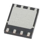
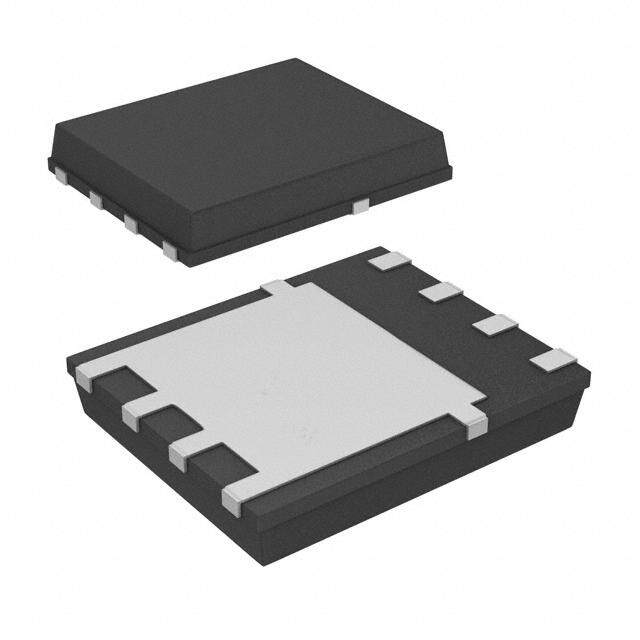
ICGOO电子元器件商城为您提供CSD17556Q5B由Texas Instruments设计生产,在icgoo商城现货销售,并且可以通过原厂、代理商等渠道进行代购。 CSD17556Q5B价格参考。Texas InstrumentsCSD17556Q5B封装/规格:晶体管 - FET,MOSFET - 单, 表面贴装 N 沟道 30V 34A(Ta),100A(Tc) 3.1W(Ta),191W(Tc) 8-VSON-CLIP(5x6)。您可以下载CSD17556Q5B参考资料、Datasheet数据手册功能说明书,资料中有CSD17556Q5B 详细功能的应用电路图电压和使用方法及教程。
CSD17556Q5B 是由 Texas Instruments(德州仪器)生产的一款增强型 N 沟道 MOSFET,属于 NexFET 系列。该器件采用小型 QFN 封装,具有低导通电阻(Rds(on))、高效率和出色的热性能,适用于多种电力电子应用场景。以下是 CSD17556Q5B 的主要应用场景:

 1. 开关电源 (SMPS)
   - 作为功率级开关,用于 DC-DC 转换器、降压/升压转换器和反激式变换器。
   - 在同步整流电路中,CSD17556Q5B 可以用作高效整流元件,降低功耗。

 2. 电机驱动
   - 用于小型直流电机或无刷直流电机(BLDC)的驱动电路,提供高效的开关控制。
   - 在 H 桥电路中,作为功率开关实现电机的正转、反转和制动。

 3. 电池管理系统 (BMS)
   - 用于电池充放电保护电路,作为开关控制电池的接入与断开。
   - 在负载切换应用中,确保快速响应和低损耗。

 4. 消费类电子产品
   - 应用于智能手机、平板电脑和其他便携式设备中的电源管理模块。
   - 用于 USB 充电器和适配器中的功率开关,支持快速充电功能。

 5. 工业自动化
   - 在工业控制系统中,用于继电器替代、负载切换和信号隔离。
   - 适用于需要高效功率转换的工业设备,如 PLC 和传感器接口。

 6. 汽车电子
   - 用于车载电子设备中的负载切换和电源管理。
   - 支持汽车环境下的高可靠性要求,例如车窗升降器、座椅调节器等。

 特性优势:
- 低导通电阻:典型值为 3.9 mΩ(在 Vgs = 10V 时),可显著降低导通损耗。
- 高工作电流:连续漏极电流高达 58 A(Tc = 25°C),满足大功率应用需求。
- 高频率性能:快速开关速度和低栅极电荷(Qg = 19 nC),适合高频应用。
- 小型封装:采用 3.3 mm × 3.3 mm QFN 封装,节省 PCB 空间。

综上所述,CSD17556Q5B 以其高性能和紧凑设计,广泛应用于消费电子、工业控制、汽车电子和通信设备等领域,特别适合对效率和空间有严格要求的设计场景。
| 参数 | 数值 |
| 产品目录 | |
| 描述 | MOSFET N-CH 30V 8-VSONMOSFET 30V N-Ch NexFET Power MOSFETs |
| 产品分类 | FET - 单分离式半导体 |
| FET功能 | 逻辑电平门 |
| FET类型 | MOSFET N 通道,金属氧化物 |
| Id-ContinuousDrainCurrent | 100 A |
| 品牌 | Texas Instruments |
| 产品手册 | http://www.ti.com/litv/slps392a |
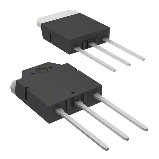
| 产品图片 |
|
| rohs | 符合RoHS含铅 / 不受限制有害物质指令(RoHS)规范要求限制 |
| 产品系列 | 晶体管,MOSFET,Texas Instruments CSD17556Q5BNexFET™ |
| 数据手册 | |
| 产品型号 | CSD17556Q5B |
| PCN组件/产地 | |
| PCN设计/规格 | |
| Pd-PowerDissipation | 3.1 W |
| Qg-GateCharge | 30 nC |
| RdsOn-Drain-SourceResistance | 1.5 mOhms |
| Vds-Drain-SourceBreakdownVoltage | 30 V |
| Vgs-Gate-SourceBreakdownVoltage | 20 V |
| Vgsth-Gate-SourceThresholdVoltage | 1.4 V |
| 上升时间 | 26 ns |
| 下降时间 | 12 ns |
| 不同Id时的Vgs(th)(最大值) | 1.65V @ 250µA |
| 不同Vds时的输入电容(Ciss) | 7020pF @ 15V |
| 不同Vgs时的栅极电荷(Qg) | 39nC @ 4.5V |
| 不同 Id、Vgs时的 RdsOn(最大值) | 1.4 毫欧 @ 40A, 10V |
| 产品种类 | MOSFET |
| 供应商器件封装 | 8-VSON (5x6) |
| 其它名称 | 296-35726-6 |
| 典型关闭延迟时间 | 27 ns |
| 功率-最大值 | 3.1W |
| 包装 | Digi-Reel® |
| 商标 | Texas Instruments |
| 商标名 | NexFET |
| 安装类型 | 表面贴装 |
| 安装风格 | SMD/SMT |
| 封装 | Reel |
| 封装/外壳 | 8-TDFN 裸露焊盘 |
| 封装/箱体 | VSON-8 Clip |
| 工厂包装数量 | 2500 |
| 晶体管极性 | N-Channel |
| 最大工作温度 | + 150 C |
| 最小工作温度 | - 55 C |
| 标准包装 | 1 |
| 正向跨导-最小值 | 197 S |
| 漏源极电压(Vdss) | 30V |
| 电流-连续漏极(Id)(25°C时) | 34A(Ta), 100A(Tc) |
| 系列 | CSD17556Q5B |
| 配置 | Dual Dual Drain |


- 商务部:美国ITC正式对集成电路等产品启动337调查
- 曝三星4nm工艺存在良率问题 高通将骁龙8 Gen1或转产台积电
- 太阳诱电将投资9.5亿元在常州建新厂生产MLCC 预计2023年完工
- 英特尔发布欧洲新工厂建设计划 深化IDM 2.0 战略
- 台积电先进制程称霸业界 有大客户加持明年业绩稳了
- 达到5530亿美元!SIA预计今年全球半导体销售额将创下新高
- 英特尔拟将自动驾驶子公司Mobileye上市 估值或超500亿美元
- 三星加码芯片和SET,合并消费电子和移动部门,撤换高东真等 CEO
- 三星电子宣布重大人事变动 还合并消费电子和移动部门
- 海关总署:前11个月进口集成电路产品价值2.52万亿元 增长14.8%


PDF Datasheet 数据手册内容提取
Product Order Technical Tools & Support & Folder Now Documents Software Community CSD17556Q5B SLPS392D–MARCH2013–REVISEDNOVEMBER2017 CSD17556Q5B 30-V N-Channel NexFET™ Power MOSFET 1 Features ProductSummary • ExtremelyLowResistance 1• Ultra-LowQ andQ TA=25°C TYPICALVALUE UNIT g gd VDS Drain-to-SourceVoltage 30 V • Low-ThermalResistance Qg GateChargeTotal(4.5V) 30 nC • AvalancheRated Qgd GateChargeGate-to-Drain 7.5 nC • Lead-FreeTerminalPlating VGS=4.5V 1.5 RDS(on) Drain-to-SourceOn-Resistance mΩ • RoHSCompliant VGS=10V 1.2 • HalogenFree VGS(th) ThresholdVoltage 1.4 V • SON5-mm×6-mmPlasticPackage DeviceInformation(1) 2 Applications DEVICE QTY MEDIA PACKAGE SHIP CSD17556Q5B 2500 SON Tape • PointofLoadSynchronousBuckinNetworking, 13-InchReel 5.00-mm×6.00-mm and CSD17556Q5BT 250 PlasticPackage Reel Telecom,andComputingSystems (1) For all available packages, see the orderable addendum at • SynchronousRectification theendofthedatasheet. • ActiveORingandHotswapApplications AbsoluteMaximumRatings 3 Description TA=25°C VALUE UNIT This 30-V, 1.2-mΩ, 5-mm × 6-mm NexFET™ power VDS Drain-to-SourceVoltage 30 V MOSFET is designed to minimize losses in VGS Gate-to-SourceVoltage ±20 V synchronous rectification and other power conversion ContinuousDrainCurrent(PackageLimited) 100 applications. ContinuousDrainCurrent(SiliconLimited), ID TC=25°C 215 A TopView ContinuousDrainCurrent(1) 34 IDM PulsedDrainCurrent,TA=25°C(1)(2) 400 A S 1 8 D PowerDissipation(1) 3.1 PD W PowerDissipation,TC=25°C 191 S 2 7 D TJ, OperatingJunction, –55to150 °C Tstg StorageTemperature S 3 6 D AvalancheEnergy,SinglePulse D EAS ID=100A,L=0.1mH,RG=25Ω 500 mJ G 4 5 D (1) Typical R = 40°C/W on 1-in2 (6.45-cm2), 2-oz θJA (0.071-mm)thickCupadona0.06-inch(1.52-mm)thickFR4 P0093-01 PCB. (2) Max R = 1.3°C/W, pulse duration ≤ 100 μs, duty cycle ≤ θJC 1%. R vsV GateCharge DS(on) GS 6 10 ) TC = 25°C Id = 30A ID = 30A We (m 5 TC = 125ºC Id = 30A ge (V) 8 VDS =15V stanc 4 Volta si e 6 e c e R 3 our n-Stat 2 e-to-S 4 O at - ()Son 1 - GGS 2 D V R 0 0 0 2 4 6 8 10 12 0 10 20 30 40 50 60 70 VGS - Gate-to- Source Voltage (V) G001 Qg - Gate Charge (nC) G001 1 An IMPORTANT NOTICE at the end of this data sheet addresses availability, warranty, changes, use in safety-critical applications, intellectualpropertymattersandotherimportantdisclaimers.PRODUCTIONDATA.
CSD17556Q5B SLPS392D–MARCH2013–REVISEDNOVEMBER2017 www.ti.com Table of Contents 1 Features.................................................................. 1 6.2 CommunityResources..............................................7 2 Applications........................................................... 1 6.3 Trademarks...............................................................7 3 Description............................................................. 1 6.4 ElectrostaticDischargeCaution................................7 6.5 Glossary....................................................................7 4 RevisionHistory..................................................... 2 7 Mechanical,Packaging,andOrderable 5 Specifications......................................................... 3 Information............................................................. 8 5.1 ElectricalCharacteristics...........................................3 7.1 Q5BPackageDimensions........................................8 5.2 ThermalInformation..................................................3 7.2 RecommendedPCBPattern.....................................9 5.3 TypicalMOSFETCharacteristics..............................4 7.3 RecommendedStencilPattern.................................9 6 DeviceandDocumentationSupport.................... 7 7.4 Q5BTapeandReelInformation.............................10 6.1 ReceivingNotificationofDocumentationUpdates....7 4 Revision History ChangesfromRevisionC(January2017)toRevisionD Page • Correctedfrontpageformattingerror..................................................................................................................................... 1 ChangesfromRevisionB(August2014)toRevisionC Page • ChangedpartnumbersintheDeviceInformationtable......................................................................................................... 1 • AddedReceivingNotificationofDocumentationUpdatessectionandCommunityResourcessectiontotheDevice andDocumentationSupportsection...................................................................................................................................... 7 ChangesfromRevisionA(October2013)toRevisionB Page • Increasedmaxpulseddraincurrentto400A........................................................................................................................ 1 • Updatedpulseddraincurrentconditions ............................................................................................................................... 1 • UpdatedFigure1toanormalizedR curve ....................................................................................................................... 4 θJC • UpdatedtheSOAinFigure10 .............................................................................................................................................. 6 • Updatedthemechanicaldrawinganddimensionstabletoshowpreviouslyunknowndimensions...................................... 8 ChangesfromOriginal(March2013)toRevisionA Page • UpdatedthedimensionstableintheMechanicalDataSectiontoincludeDIM"H"values................................................... 8 2 SubmitDocumentationFeedback Copyright©2013–2017,TexasInstrumentsIncorporated ProductFolderLinks:CSD17556Q5B
CSD17556Q5B www.ti.com SLPS392D–MARCH2013–REVISEDNOVEMBER2017 5 Specifications 5.1 Electrical Characteristics T =25°C(unlessotherwisestated) A PARAMETER TESTCONDITIONS MIN TYP MAX UNIT STATICCHARACTERISTICS BV Drain-to-sourcevoltage V =0V,I =250μA 30 V DSS GS DS I Drain-to-sourceleakagecurrent V =0V,V =24V 1 μA DSS GS DS I Gate-to-sourceleakagecurrent V =0V,V =20V 100 nA GSS DS GS V Gate-to-sourcethresholdvoltage V =V ,I =250μA 1.15 1.4 1.65 V GS(th) DS GS DS V =4.5V,I =40A 1.5 1.8 GS DS R Drain-to-sourceon-resistance mΩ DS(on) V =10V,I =40A 1.2 1.4 GS DS g Transconductance V =15V,I =40A 197 S fs DS DS DYNAMICCHARACTERISTICS C Inputcapacitance 5400 7020 pF iss V =0V,V =15V, C Outputcapacitance GS DS 1770 2310 pF oss ƒ=1MHz C Reversetransfercapacitance 68 88 pF rss R Seriesgateresistance 0.7 1.4 Ω G Q Gatechargetotal(4.5V) 30 39 nC g Q Gatechargegate-to-drain 7.5 nC gd V =15V,I =40A DS DS Q Gatechargegate-to-source 11 nC gs Q GatechargeatV 6.1 nC g(th) th Q Outputcharge V =15V,V =0V 48 nC oss DS GS t Turnondelaytime 14 ns d(on) tr Risetime VDS=15V,VGS=4.5V, 26 ns td(off) Turnoffdelaytime IDS=40A,RG=2Ω 27 ns t Falltime 12 ns f DIODECHARACTERISTICS V Diodeforwardvoltage I =40A,V =0V 0.8 1 V SD SD GS Q Reverserecoverycharge 68 nC rr V =15V,I =40A,di/dt=300A/μs DD F t Reverserecoverytime 36 ns rr 5.2 Thermal Information T =25°C(unlessotherwisestated) A THERMALMETRIC MIN TYP MAX UNIT R Junction-to-casethermalresistance(1) 1.3 θJC °C/W R Junction-to-ambientthermalresistance(1)(2) 50 θJA (1) R isdeterminedwiththedevicemountedona1-in2(6.45-cm2),2-oz(0.071-mm)thickCupadona1.5-in×1.5-in θJC (3.81-cm×3.81-cm),0.06-in(1.52-mm)thickFR4PCB.R isspecifiedbydesign,whereasR isdeterminedbytheuser’sboard θJC θJA design. (2) DevicemountedonFR4materialwith1-in2(6.45-cm2),2-oz(0.071-mm)thickCu. Copyright©2013–2017,TexasInstrumentsIncorporated SubmitDocumentationFeedback 3 ProductFolderLinks:CSD17556Q5B
CSD17556Q5B SLPS392D–MARCH2013–REVISEDNOVEMBER2017 www.ti.com GATE Source GATE Source N N - - C C h h a a n n MaxR =50°C/W MaxR =125°C/W 5x θJA 5x θJA 6 whenmountedon1-in2 6 whenmountedona Q Q FN (6.45-cm2)of FN minimumpadareaof TT 2-oz(0.071-mm)thick TT 2-oz(0.071-mm)thick A A M Cu. M Cu. A I X N R R e e v v 3 DRAIN 3 DRAIN M0137-01 M0137-02 5.3 Typical MOSFET Characteristics T =25°C(unlessotherwisestated) A Figure1.TransientThermalImpedance 4 SubmitDocumentationFeedback Copyright©2013–2017,TexasInstrumentsIncorporated ProductFolderLinks:CSD17556Q5B
CSD17556Q5B www.ti.com SLPS392D–MARCH2013–REVISEDNOVEMBER2017 Typical MOSFET Characteristics (continued) T =25°C(unlessotherwisestated) A 200 200 A) 180 A) 180 VDS = 5V nt ( 160 nt ( 160 e e urr 140 urr 140 C C e 120 e 120 c c our 100 our 100 S S o- 80 o- 80 n-t n-t ai 60 ai 60 Dr Dr I - DS 2400 VVVGGGSSS ===1640V.5VV I - DS 2400 TTTCCC === 12−2555°5C°°CC 0 0 0 0.1 0.2 0.3 0.4 0.5 0 1 2 3 4 5 VDS - Drain-to-Source Voltage (V) G001 VGS - Gate-to-Source Voltage (V) G001 Figure2.SaturationCharacteristics Figure3.TransferCharacteristics 10 100000 ID = 30A Ciss = Cgd + Cgs e-to-Source Voltage (V) 468 VDS =15V Capacitance (pF) 110000000 CCorssss == CCdgsd + Cgd at − G C 100 - S 2 G V 0 10 0 10 20 30 40 50 60 70 0 10 20 30 Qg - Gate Charge (nC) G001 VDS - Drain-to-Source Voltage (V) G001 Figure4.GateCharge Figure5.Capacitance 2 6 ID = 250uA ) TC = 25°C Id = 30A V) 1.8 Wm 5 TC = 125ºC Id = 30A e ( e ( d Voltag 11..46 esistanc 4 hol e R 3 es 1.2 at hr St V - T()GSth 0.81 - On-()Son 12 D R 0.6 0 −75 −25 25 75 125 175 0 2 4 6 8 10 12 TC - Case Temperature (ºC) G001 VGS - Gate-to- Source Voltage (V) G001 Figure6.ThresholdVoltagevsTemperature Figure7.On-StateResistancevsGate-to-SourceVoltage Copyright©2013–2017,TexasInstrumentsIncorporated SubmitDocumentationFeedback 5 ProductFolderLinks:CSD17556Q5B
CSD17556Q5B SLPS392D–MARCH2013–REVISEDNOVEMBER2017 www.ti.com Typical MOSFET Characteristics (continued) T =25°C(unlessotherwisestated) A 2.2 100 VGS = 4.5V ID =30A TC = 25°C stance 1.82 VGS = 10V ent (A) 10 TC = 125°C Resi 1.6 Curr 1 e n Stat 1.4 Drai 0.1 n- 1.2 o- ormalized O 0.81 − Source-tD 0.00.0011 N 0.6 S I 0.4 0.0001 −75 −25 25 75 125 175 0 0.2 0.4 0.6 0.8 1 TC - Case Temperature (ºC) G001 VSD − Source-to-Drain Voltage (V) G001 Figure8.NormalizedOn-StateResistancevsTemperature Figure9.TypicalDiodeForwardVoltage 5000 300 10us 1ms DC TC = 25ºC nt (A)1000 100us 10ms nt (A) TC = 125ºC e e urr urr 100 C 100 C e e c h ur nc o a ain-to-S 10 ak Aval - DrDS 1 Single Pulse - PeAV I Max RthetaJC = 1.3ºC/W I 0.1 10 0.1 1 10 100 0.01 0.1 1 VDS - Drain-to-Source Voltage (V) G001 TAV - Time in Avalanche (mS) G001 Figure10.MaximumSafeOperatingArea(SOA) Figure11.SinglePulseUnclampedInductiveSwitching 300.0 Silicon limited A) Package limited nt ( 250.0 e Curr 200.0 e c ur o 150.0 S o- n- t 100.0 ai Dr - S 50.0 D I 0.0 −50 −25 0 25 50 75 100 125 150 175 TC - Case Temperature (ºC) G001 Figure12.MaximumDrainCurrentvsTemperature 6 SubmitDocumentationFeedback Copyright©2013–2017,TexasInstrumentsIncorporated ProductFolderLinks:CSD17556Q5B
CSD17556Q5B www.ti.com SLPS392D–MARCH2013–REVISEDNOVEMBER2017 6 Device and Documentation Support 6.1 Receiving Notification of Documentation Updates To receive notification of documentation updates, navigate to the device product folder on ti.com. In the upper right corner, click on Alert me to register and receive a weekly digest of any product information that has changed.Forchangedetails,reviewtherevisionhistoryincludedinanyreviseddocument. 6.2 Community Resources The following links connect to TI community resources. Linked contents are provided "AS IS" by the respective contributors. They do not constitute TI specifications and do not necessarily reflect TI's views; see TI's Terms of Use. TIE2E™OnlineCommunity TI'sEngineer-to-Engineer(E2E)Community.Createdtofostercollaboration amongengineers.Ate2e.ti.com,youcanaskquestions,shareknowledge,exploreideasandhelp solveproblemswithfellowengineers. DesignSupport TI'sDesignSupport QuicklyfindhelpfulE2Eforumsalongwithdesignsupporttoolsand contactinformationfortechnicalsupport. 6.3 Trademarks NexFET,E2EaretrademarksofTexasInstruments. Allothertrademarksarethepropertyoftheirrespectiveowners. 6.4 Electrostatic Discharge Caution Thesedeviceshavelimitedbuilt-inESDprotection.Theleadsshouldbeshortedtogetherorthedeviceplacedinconductivefoam duringstorageorhandlingtopreventelectrostaticdamagetotheMOSgates. 6.5 Glossary SLYZ022—TIGlossary. Thisglossarylistsandexplainsterms,acronyms,anddefinitions. Copyright©2013–2017,TexasInstrumentsIncorporated SubmitDocumentationFeedback 7 ProductFolderLinks:CSD17556Q5B
CSD17556Q5B SLPS392D–MARCH2013–REVISEDNOVEMBER2017 www.ti.com 7 Mechanical, Packaging, and Orderable Information The following pages include mechanical, packaging, and orderable information. This information is the most current data available for the designated devices. This data is subject to change without notice and revision of thisdocument.Forbrowser-basedversionsofthisdatasheet,refertotheleft-handnavigation. 7.1 Q5B Package Dimensions K E1 c1 H L 8 1 8x) 1 8 (cid:127) b ( 7 2 2 7 1 D2 D3 E D 6 3 3 6 e 5 4 5 4 d1 d2 Top View Side View Bottom View (cid:127) Front View MILLIMETERS DIM MIN NOM MAX A 0.80 1.00 1.05 b 0.36 0.41 0.46 c 0.15 0.20 0.25 c1 0.15 0.20 0.25 c2 0.20 0.25 0.30 D1 4.90 5.00 5.10 D2 4.12 4.22 4.32 D3 3.90 4.00 4.10 d 0.20 0.25 0.30 d1 0.085TYP d2 0.319 0.369 0.419 E 4.90 5.00 5.10 E1 5.90 6.00 6.10 E2 3.48 3.58 3.68 e 1.27TYP H 0.36 0.46 0.56 L 0.46 0.56 0.66 L1 0.57 0.67 0.77 θ 0° — — K 1.40TYP 8 SubmitDocumentationFeedback Copyright©2013–2017,TexasInstrumentsIncorporated ProductFolderLinks:CSD17556Q5B
CSD17556Q5B www.ti.com SLPS392D–MARCH2013–REVISEDNOVEMBER2017 7.2 Recommended PCB Pattern For recommended circuit layout for PCB designs, see Reducing Ringing Through PCB Layout Techniques (SLPA005). 7.3 Recommended Stencil Pattern (0.020) (0.014) 0.508 (0.022) (0.011) 0.350 (0.029) x4 0.562 x 4 0.286 0.746 x 8 2.186(0.086) 4.318(0.170) 0.300 (0.012) 1.270 (0.050) 1.270(0.050) (0.051) (0.030) 1.294 (0.060) 0.766 (0.042) x 8 1.525 1.072 (0.259) 6.586 Copyright©2013–2017,TexasInstrumentsIncorporated SubmitDocumentationFeedback 9 ProductFolderLinks:CSD17556Q5B
CSD17556Q5B SLPS392D–MARCH2013–REVISEDNOVEMBER2017 www.ti.com 7.4 Q5B Tape and Reel Information 0 1 K0 0. ± 0.30 ±0.05 4.00 ±0.10 (See Note 1) 5 7 2.00 ±0.05 Ø 1.50 +0.10 1. –0.00 0 3 0. ± 0 B0 2.0 1 5 0 0. ± 0 5 5. A0 8.00 ±0.10 R 0.30 MAX Ø 1.50 MIN R 0.30TYP A0 = 6.50 ±0.10 B0 = 5.30 ±0.10 K0 = 1.40 ±0.10 M0138-01 Notes: 1. 10-sprockethole-pitchcumulativetolerance±0.2. 2. Cambernottoexceed1mmin100mm,noncumulativeover250mm. 3. Material:blackstatic-dissipativepolystyrene. 4. Alldimensionsareinmm(unlessotherwisespecified). 5. A0andB0measuredonaplane0.3mmabovethebottomofthepocket. 10 SubmitDocumentationFeedback Copyright©2013–2017,TexasInstrumentsIncorporated ProductFolderLinks:CSD17556Q5B
PACKAGE OPTION ADDENDUM www.ti.com 6-Feb-2020 PACKAGING INFORMATION Orderable Device Status Package Type Package Pins Package Eco Plan Lead/Ball Finish MSL Peak Temp Op Temp (°C) Device Marking Samples (1) Drawing Qty (2) (6) (3) (4/5) CSD17556Q5B ACTIVE VSON-CLIP DNK 8 2500 Pb-Free (RoHS SN Level-1-260C-UNLIM -55 to 150 CSD17556 Exempt) CSD17556Q5BT ACTIVE VSON-CLIP DNK 8 250 Pb-Free (RoHS SN Level-1-260C-UNLIM -55 to 150 CSD17556 Exempt) (1) The marketing status values are defined as follows: ACTIVE: Product device recommended for new designs. LIFEBUY: TI has announced that the device will be discontinued, and a lifetime-buy period is in effect. NRND: Not recommended for new designs. Device is in production to support existing customers, but TI does not recommend using this part in a new design. PREVIEW: Device has been announced but is not in production. Samples may or may not be available. OBSOLETE: TI has discontinued the production of the device. (2) RoHS: TI defines "RoHS" to mean semiconductor products that are compliant with the current EU RoHS requirements for all 10 RoHS substances, including the requirement that RoHS substance do not exceed 0.1% by weight in homogeneous materials. Where designed to be soldered at high temperatures, "RoHS" products are suitable for use in specified lead-free processes. TI may reference these types of products as "Pb-Free". RoHS Exempt: TI defines "RoHS Exempt" to mean products that contain lead but are compliant with EU RoHS pursuant to a specific EU RoHS exemption. Green: TI defines "Green" to mean the content of Chlorine (Cl) and Bromine (Br) based flame retardants meet JS709B low halogen requirements of <=1000ppm threshold. Antimony trioxide based flame retardants must also meet the <=1000ppm threshold requirement. (3) MSL, Peak Temp. - The Moisture Sensitivity Level rating according to the JEDEC industry standard classifications, and peak solder temperature. (4) There may be additional marking, which relates to the logo, the lot trace code information, or the environmental category on the device. (5) Multiple Device Markings will be inside parentheses. Only one Device Marking contained in parentheses and separated by a "~" will appear on a device. If a line is indented then it is a continuation of the previous line and the two combined represent the entire Device Marking for that device. (6) Lead/Ball Finish - Orderable Devices may have multiple material finish options. Finish options are separated by a vertical ruled line. Lead/Ball Finish values may wrap to two lines if the finish value exceeds the maximum column width. Important Information and Disclaimer:The information provided on this page represents TI's knowledge and belief as of the date that it is provided. TI bases its knowledge and belief on information provided by third parties, and makes no representation or warranty as to the accuracy of such information. Efforts are underway to better integrate information from third parties. TI has taken and continues to take reasonable steps to provide representative and accurate information but may not have conducted destructive testing or chemical analysis on incoming materials and chemicals. TI and TI suppliers consider certain information to be proprietary, and thus CAS numbers and other limited information may not be available for release. In no event shall TI's liability arising out of such information exceed the total purchase price of the TI part(s) at issue in this document sold by TI to Customer on an annual basis. Addendum-Page 1
PACKAGE OPTION ADDENDUM www.ti.com 6-Feb-2020 Addendum-Page 2
IMPORTANTNOTICEANDDISCLAIMER TI PROVIDES TECHNICAL AND RELIABILITY DATA (INCLUDING DATASHEETS), DESIGN RESOURCES (INCLUDING REFERENCE DESIGNS), APPLICATION OR OTHER DESIGN ADVICE, WEB TOOLS, SAFETY INFORMATION, AND OTHER RESOURCES “AS IS” AND WITH ALL FAULTS, AND DISCLAIMS ALL WARRANTIES, EXPRESS AND IMPLIED, INCLUDING WITHOUT LIMITATION ANY IMPLIED WARRANTIES OF MERCHANTABILITY, FITNESS FOR A PARTICULAR PURPOSE OR NON-INFRINGEMENT OF THIRD PARTY INTELLECTUAL PROPERTY RIGHTS. These resources are intended for skilled developers designing with TI products. You are solely responsible for (1) selecting the appropriate TI products for your application, (2) designing, validating and testing your application, and (3) ensuring your application meets applicable standards, and any other safety, security, or other requirements. These resources are subject to change without notice. TI grants you permission to use these resources only for development of an application that uses the TI products described in the resource. Other reproduction and display of these resources is prohibited. No license is granted to any other TI intellectual property right or to any third party intellectual property right. TI disclaims responsibility for, and you will fully indemnify TI and its representatives against, any claims, damages, costs, losses, and liabilities arising out of your use of these resources. TI’s products are provided subject to TI’s Terms of Sale (www.ti.com/legal/termsofsale.html) or other applicable terms available either on ti.com or provided in conjunction with such TI products. TI’s provision of these resources does not expand or otherwise alter TI’s applicable warranties or warranty disclaimers for TI products. Mailing Address: Texas Instruments, Post Office Box 655303, Dallas, Texas 75265 Copyright © 2020, Texas Instruments Incorporated