ICGOO在线商城 > 分立半导体产品 > 晶体管 - FET,MOSFET - 单 > BS108ZL1G
 Datasheet下载
- 型号: BS108ZL1G
- 制造商: ON Semiconductor
- 库位|库存: xxxx|xxxx
- 要求:
| 数量阶梯 | 香港交货 | 国内含税 |
| +xxxx | $xxxx | ¥xxxx |
查看当月历史价格
查看今年历史价格
BS108ZL1G产品简介:
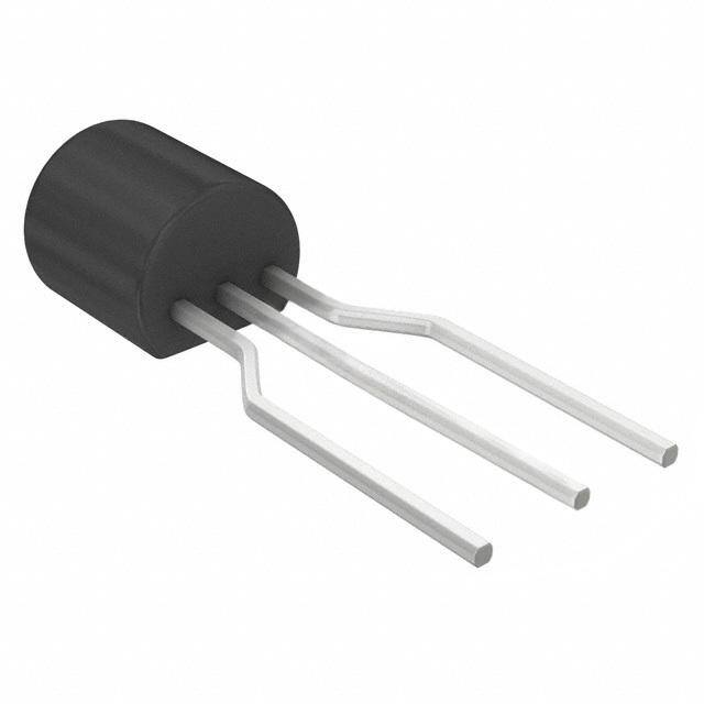
ICGOO电子元器件商城为您提供BS108ZL1G由ON Semiconductor设计生产,在icgoo商城现货销售,并且可以通过原厂、代理商等渠道进行代购。 BS108ZL1G价格参考。ON SemiconductorBS108ZL1G封装/规格:晶体管 - FET,MOSFET - 单, N-Channel 200V 250mA (Ta) 350mW (Ta) Through Hole TO-92-3。您可以下载BS108ZL1G参考资料、Datasheet数据手册功能说明书,资料中有BS108ZL1G 详细功能的应用电路图电压和使用方法及教程。
ON Semiconductor的BS108ZL1G是一款N沟道增强型MOSFET,属于小信号MOSFET,广泛应用于低电压、低功率开关场景。其主要特点包括低栅极电荷、快速开关响应和小型SOT-23封装,适合空间受限的便携式设备。

典型应用场景包括:
1. 便携式电子产品:如智能手机、平板电脑和可穿戴设备中的电源管理与负载开关,用于控制不同模块的供电通断,降低功耗。
2. 电池供电设备:在蓝牙耳机、无线传感器、遥控器等产品中作为高效开关元件,实现电池与负载之间的连接控制,提升能效。
3. 逻辑电平转换电路:用于不同电压域之间的信号切换,例如将3.3V逻辑信号转换为5V系统可用信号,适用于微控制器接口设计。
4. LED驱动与控制:在低电流LED指示灯或背光控制中作为开关,实现精确的亮灭控制。
5. 电源多路复用与热插拔保护:在小型电源管理系统中用于防止反向电流或实现冗余电源切换。

由于其低导通电阻(RDS(on))和良好的热稳定性,BS108ZL1G在高密度PCB布局中表现出色,同时具备较高的可靠性,适用于消费电子、工业控制及通信设备中的信号与电源开关应用。
| 参数 | 数值 |
| 产品目录 | |
| ChannelMode | Enhancement |
| 描述 | MOSFET N-CH 200V 250MA TO-92MOSFET 200V 250mA Logic Level N-Channel |
| 产品分类 | FET - 单分离式半导体 |
| FET功能 | 逻辑电平门 |
| FET类型 | MOSFET N 通道,金属氧化物 |
| Id-ContinuousDrainCurrent | 250 mA |
| Id-连续漏极电流 | 250 mA |
| 品牌 | ON Semiconductor |
| 产品手册 | |
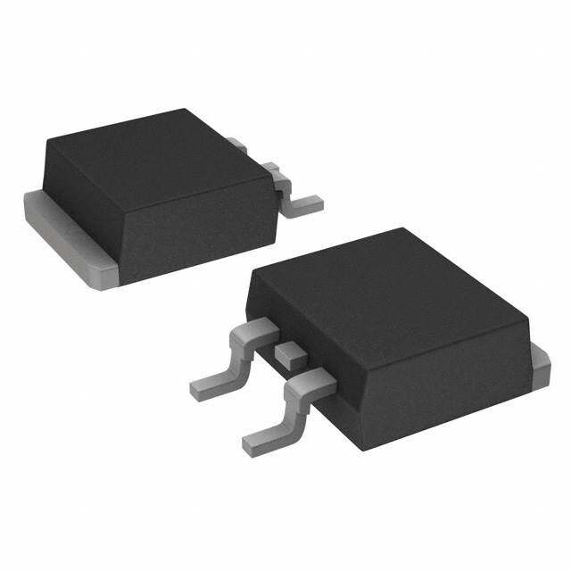
| 产品图片 |
|
| rohs | 符合RoHS无铅 / 符合限制有害物质指令(RoHS)规范要求 |
| 产品系列 | 晶体管,MOSFET,ON Semiconductor BS108ZL1G- |
| 数据手册 | |
| 产品型号 | BS108ZL1G |
| Pd-PowerDissipation | 0.35 W |
| Pd-功率耗散 | 350 mW |
| RdsOn-Drain-SourceResistance | 8 Ohms |
| RdsOn-漏源导通电阻 | 8 Ohms |
| Vds-Drain-SourceBreakdownVoltage | 200 V |
| Vds-漏源极击穿电压 | 200 V |
| Vgs-Gate-SourceBreakdownVoltage | +/- 20 V |
| Vgs-栅源极击穿电压 | 20 V |
| 不同Id时的Vgs(th)(最大值) | 1.5V @ 1mA |
| 不同Vds时的输入电容(Ciss) | 150pF @ 25V |
| 不同Vgs时的栅极电荷(Qg) | - |
| 不同 Id、Vgs时的 RdsOn(最大值) | 8 欧姆 @ 100mA,2.8V |
| 产品种类 | MOSFET |
| 供应商器件封装 | TO-92-3 |
| 其它名称 | BS108ZL1GOSCT |
| 典型关闭延迟时间 | 15 ns |
| 功率-最大值 | 350mW |
| 功率耗散 | 0.35 W |
| 包装 | 剪切带 (CT) |
| 商标 | ON Semiconductor |
| 安装类型 | 通孔 |
| 安装风格 | Through Hole |
| 导通电阻 | 8 Ohms |
| 封装 | Ammo Pack |
| 封装/外壳 | TO-226-3、TO-92-3(TO-226AA)成形引线 |
| 封装/箱体 | TO-92-3 |
| 工厂包装数量 | 2000 |
| 晶体管极性 | N-Channel |
| 最大工作温度 | + 150 C |
| 最小工作温度 | - 55 C |
| 标准包装 | 1 |
| 正向跨导-最小值 | 0.33 S |
| 汲极/源极击穿电压 | 200 V |
| 漏极连续电流 | 250 mA |
| 漏源极电压(Vdss) | 200V |
| 电流-连续漏极(Id)(25°C时) | 250mA (Ta) |
| 系列 | BS108 |
| 通道模式 | Enhancement |
| 配置 | Single |
| 闸/源击穿电压 | +/- 20 V |

,TO-226_straightlead.jpg)


PDF Datasheet 数据手册内容提取
BS108 Small Signal MOSFET 250 mAmps, 200 Volts, Logic Level N−Channel TO−92 http://onsemi.com This MOSFET is designed for high voltage, high speed switching 250 mAMPS applications such as line drivers, relay drivers, CMOS logic, 200 VOLTS microprocessor or TTL to high voltage interface and high voltage display drivers. R = 8 (cid:3) DS(on) Features • N−Channel Low Drive Requirement, V = 3.0 V max GS • D Inherent Current Sharing Capability Permits Easy Paralleling of many Devices • AEC Qualified • PPAP Capable G • This is a Pb−Free Device* S MAXIMUM RATINGS Rating Symbol Value Unit MARKING Drain−Source Voltage VDSS 200 Vdc DIAGRAM Gate−Source Voltage VGS ±20 Vdc Drain Current mAdc A Continuous (Note 1) ID 250 BS108 Pulsed (Note 2) IDM 500 YWW(cid:2) TO−92 (cid:2) Total Power Dissipation PD 1 CASE 29−11 @ TA = 25°C 350 mW 2 STYLE 30 Derate above TA = 25°C 6.4 mW/°C 3 Operating and Storage Temperature Range TJ, Tstg −55 to +150 °C Stresses exceeding Maximum Ratings may damage the device. Maximum BS108 = Device Code Ratings are stress ratings only. Functional operation above the Recommended A = Assembly Location Operating Conditions is not implied. Extended exposure to stresses above the Y = Year Recommended Operating Conditions may affect device reliability. WW = Work Week 1. The Power Dissipation of the package may result in a lower continuous drain current. (cid:2) = Pb−Free Package 2. Pulse Test: Pulse Width (cid:2) 300 (cid:2)s, Duty Cycle (cid:2) 2.0%. (Note: Microdot may be in either location) ORDERING INFORMATION Device Package Shipping BS108ZL1G TO−92 2000/Ammo Pack (Pb−Free) *For additional information on our Pb−Free strategy and soldering details, please download the ON Semiconductor Soldering and Mounting Techniques Reference Manual, SOLDERRM/D. © Semiconductor Components Industries, LLC, 2011 1 Publication Order Number: April, 2011 − Rev. 4 BS108/D
BS108 ELECTRICAL CHARACTERISTICS (TC = 25°C unless otherwise noted) Characteristic Symbol Min Typ Max Unit OFF CHARACTERISTICS Drain−Source Breakdown Voltage V(BR)DS − Vdc (VGS = 0, ID = 10 (cid:2)A) 200 − − Zero Gate Voltage Drain Current IDSS nAdc (VDSS = 130 Vdc, VGS = 0) − − 30 Gate−Body Leakage Current IGSSF nAdc (VGS = 15 Vdc, VDS = 0) − − 10 ON CHARACTERISTICS (Note 3) Gate Threshold Voltage VGS(th) Vdc (ID = 1.0 mA, VDS = VGS) 0.5 − 1.5 Static Drain−to−Source On−Resistance rDS(on) (cid:3) (VGS = 2.0 Vdc, ID = 50 mA) − − 10 (VGS = 2.8 Vdc, ID = 100 mA) − − 8.0 Drain Cutoff Current IDSX (cid:2)A (VGS = 0.2 V, VDS = 70 V) − − 25 Forward Transconductance gFS Mhos (ID = 120 mA, VDS = 20 V) − 0.33 − DYNAMIC CHARACTERISTICS Input Capacitance Ciss pF (VDS = 25 V, VGS = 0, f = 1.0 MHz) − − 150 Output Capacitance Coss pF (VDS = 25 V, VGS = 0, f = 1.0 MHz) − − 30 Reverse Transfer Capacitance Crss pF (VDS = 25 V, VGS = 0, f = 1.0 MHz) − − 10 SWITCHING CHARACTERISTICS Turn−On Time (See Figure 1) td(on) − − 15 ns Turn−Off Time (See Figure 1) td(off) − − 15 ns 3. Pulse Test: Pulse Width ≤300 (cid:2)s, Duty Cycle =2.0%. RESISTIVE SWITCHING +25 V TO SAMPLING SCOPE ton toff 23 50 (cid:3) INPUT PULSE GENERATOR Vin 50 (cid:3) AT2T0 EdNBUATOR Vout 90% 90% 40 pF 50 OUTPUT 10% 50 1.0 M INVERTED Vout 90% 10 V 50% PULSE 50% WIDTH INPUT Vin 10% Figure 1. Switching Test Circuit Figure 2. Switching Waveforms http://onsemi.com 2
BS108 PACKAGE DIMENSIONS TO−92 (TO−226) CASE 29−11 ISSUE AM A NOTES: B STRAIGHT LEAD 1. DIMENSIONING AND TOLERANCING PER ANSI BULK PACK Y14.5M, 1982. 2. CONTROLLING DIMENSION: INCH. R 3. CONTOUR OF PACKAGE BEYOND DIMENSION R IS UNCONTROLLED. 4. LEAD DIMENSION IS UNCONTROLLED IN P AND P BEYOND DIMENSION K MINIMUM. L SEATING INCHES MILLIMETERS PLANE K DIM MIN MAX MIN MAX A 0.175 0.205 4.45 5.20 B 0.170 0.210 4.32 5.33 C 0.125 0.165 3.18 4.19 D 0.016 0.021 0.407 0.533 X X D G 0.045 0.055 1.15 1.39 G H 0.095 0.105 2.42 2.66 J 0.015 0.020 0.39 0.50 H J K 0.500 --- 12.70 --- L 0.250 --- 6.35 --- V C N 0.080 0.105 2.04 2.66 P --- 0.100 --- 2.54 SECTION X−X R 0.115 --- 2.93 --- 1 N V 0.135 --- 3.43 --- N R A B BENT LEAD N1O.TEDSIM:ENSIONING AND TOLERANCING PER TAPE & REEL ASME Y14.5M, 1994. 2. CONTROLLING DIMENSION: MILLIMETERS. AMMO PACK 3. CONTOUR OF PACKAGE BEYOND DIMENSION R IS UNCONTROLLED. 4. LEAD DIMENSION IS UNCONTROLLED IN P P AND BEYOND DIMENSION K MINIMUM. T MILLIMETERS SPELAATNIENG K DIM MIN MAX A 4.45 5.20 B 4.32 5.33 C 3.18 4.19 D 0.40 0.54 STYLE 30: X X D G 2.40 2.80 PIN 1. DRAIN G KJ 120..7309 0-.-5-0 23.. GSOATUERCE J N 2.04 2.66 V P 1.50 4.00 C R 2.93 --- V 3.43 --- SECTION X−X 1 N ON Semiconductor and are registered trademarks of Semiconductor Components Industries, LLC (SCILLC). SCILLC reserves the right to make changes without further notice to any products herein. SCILLC makes no warranty, representation or guarantee regarding the suitability of its products for any particular purpose, nor does SCILLC assume any liability arising out of the application or use of any product or circuit, and specifically disclaims any and all liability, including without limitation special, consequential or incidental damages. “Typical” parameters which may be provided in SCILLC data sheets and/or specifications can and do vary in different applications and actual performance may vary over time. All operating parameters, including “Typicals” must be validated for each customer application by customer’s technical experts. SCILLC does not convey any license under its patent rights nor the rights of others. SCILLC products are not designed, intended, or authorized for use as components in systems intended for surgical implant into the body, or other applications intended to support or sustain life, or for any other application in which the failure of the SCILLC product could create a situation where personal injury or death may occur. Should Buyer purchase or use SCILLC products for any such unintended or unauthorized application, Buyer shall indemnify and hold SCILLC and its officers, employees, subsidiaries, affiliates, and distributors harmless against all claims, costs, damages, and expenses, and reasonable attorney fees arising out of, directly or indirectly, any claim of personal injury or death associated with such unintended or unauthorized use, even if such claim alleges that SCILLC was negligent regarding the design or manufacture of the part. SCILLC is an Equal Opportunity/Affirmative Action Employer. This literature is subject to all applicable copyright laws and is not for resale in any manner. PUBLICATION ORDERING INFORMATION LITERATURE FULFILLMENT: N. American Technical Support: 800−282−9855 Toll Free ON Semiconductor Website: www.onsemi.com Literature Distribution Center for ON Semiconductor USA/Canada P.O. Box 5163, Denver, Colorado 80217 USA Europe, Middle East and Africa Technical Support: Order Literature: http://www.onsemi.com/orderlit Phone: 303−675−2175 or 800−344−3860 Toll Free USA/Canada Phone: 421 33 790 2910 Fax: 303−675−2176 or 800−344−3867 Toll Free USA/Canada Japan Customer Focus Center For additional information, please contact your local Email: orderlit@onsemi.com Phone: 81−3−5773−3850 Sales Representative http://onsemi.com BS108/D 3