ICGOO在线商城 > 分立半导体产品 > 晶体管 - FET,MOSFET - 单 > AOB414
 Datasheet下载
- 型号: AOB414
- 制造商: ALPHA&OMEGA
- 库位|库存: xxxx|xxxx
- 要求:
| 数量阶梯 | 香港交货 | 国内含税 |
| +xxxx | $xxxx | ¥xxxx |
查看当月历史价格
查看今年历史价格
AOB414产品简介:
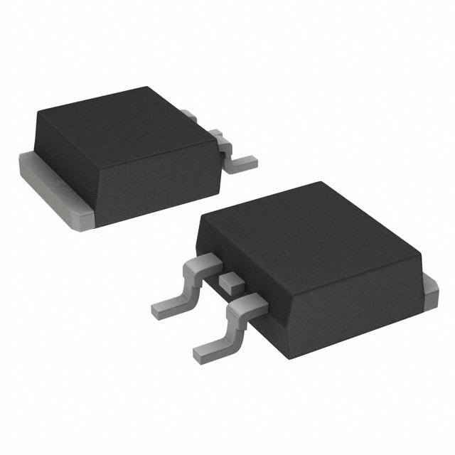
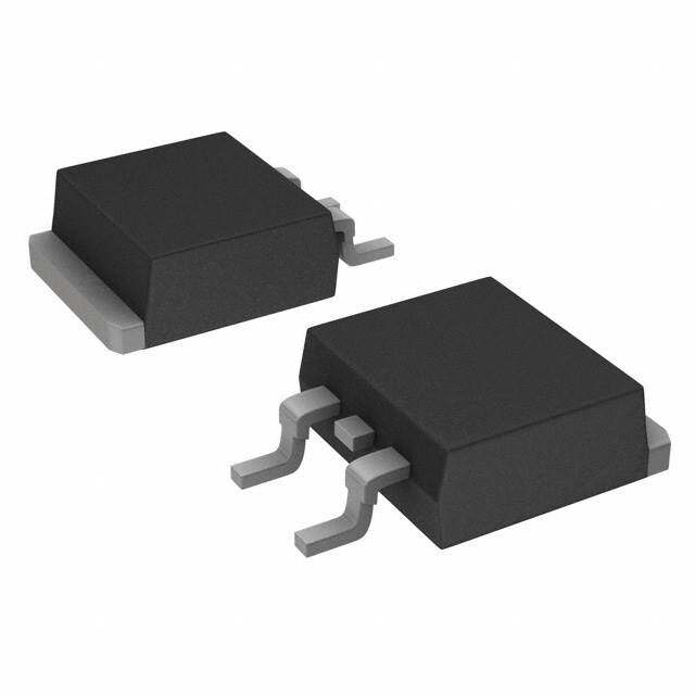
ICGOO电子元器件商城为您提供AOB414由ALPHA&OMEGA设计生产,在icgoo商城现货销售,并且可以通过原厂、代理商等渠道进行代购。 AOB414价格参考¥9.41-¥9.91。ALPHA&OMEGAAOB414封装/规格:晶体管 - FET,MOSFET - 单, 表面贴装 N 沟道 100V 6.6A(Ta),51A(Tc) 2.5W(Ta),150W(Tc) TO-263(D²Pak)。您可以下载AOB414参考资料、Datasheet数据手册功能说明书,资料中有AOB414 详细功能的应用电路图电压和使用方法及教程。
AOB414 是 Alpha & Omega Semiconductor Inc. 生产的一款 N 沟道增强型 MOSFET,常用于电源管理和功率转换应用。该器件具有低导通电阻、高效率和良好热性能,适用于以下场景:

1. DC-DC 转换器:用于笔记本电脑、服务器和通信设备中的电压调节模块(VRM),实现高效电能转换。

2. 负载开关:在电池供电设备中控制电源通断,如智能手机、平板电脑和便携式电子设备。

3. 马达驱动:用于小型电机控制电路,如无人机、机器人和电动工具。

4. 电源管理模块:作为高效开关元件,用于电源适配器、充电器和节能照明系统。

5. 同步整流:在反激式或正激式开关电源中替代传统二极管,提高转换效率。

该 MOSFET 封装小巧,适合高密度 PCB 设计,广泛应用于消费电子、工业控制和通信设备中,以实现高效、低功耗的功率管理解决方案。
| 参数 | 数值 |
| 产品目录 | |
| 描述 | MOSFET N-CH 100V 51A D2PAK |
| 产品分类 | FET - 单 |
| FET功能 | 标准 |
| FET类型 | MOSFET N 通道,金属氧化物 |
| 品牌 | Alpha & Omega Semiconductor Inc |
| 数据手册 | |
| 产品图片 |
|
| 产品型号 | AOB414 |
| rohs | 无铅 / 符合限制有害物质指令(RoHS)规范要求 |
| 产品系列 | SDMOS™ |
| 不同Id时的Vgs(th)(最大值) | 4V @ 250µA |
| 不同Vds时的输入电容(Ciss) | 2200pF @ 50V |
| 不同Vgs时的栅极电荷(Qg) | 34nC @ 10V |
| 不同 Id、Vgs时的 RdsOn(最大值) | 25 毫欧 @ 20A,10V |
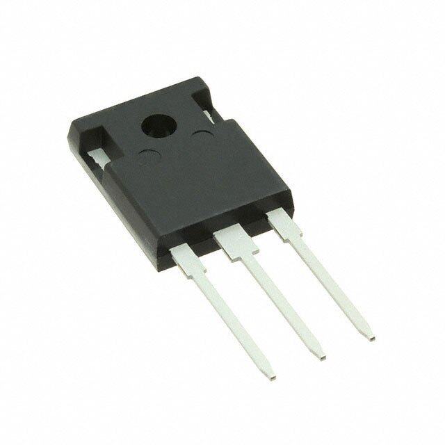
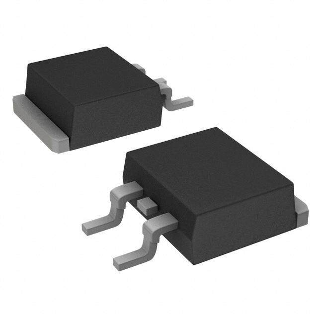
| 供应商器件封装 | TO-263(D2Pak) |
| 其它名称 | 785-1209-6 |
| 功率-最大值 | 2.5W |
| 包装 | Digi-Reel® |
| 安装类型 | 表面贴装 |
| 封装/外壳 | TO-263-3,D²Pak(2 引线+接片),TO-263AB |
| 标准包装 | 1 |
| 漏源极电压(Vdss) | 100V |
| 电流-连续漏极(Id)(25°C时) | 6.6A (Ta), 51A (Tc) |


- 商务部:美国ITC正式对集成电路等产品启动337调查
- 曝三星4nm工艺存在良率问题 高通将骁龙8 Gen1或转产台积电
- 太阳诱电将投资9.5亿元在常州建新厂生产MLCC 预计2023年完工
- 英特尔发布欧洲新工厂建设计划 深化IDM 2.0 战略
- 台积电先进制程称霸业界 有大客户加持明年业绩稳了
- 达到5530亿美元!SIA预计今年全球半导体销售额将创下新高
- 英特尔拟将自动驾驶子公司Mobileye上市 估值或超500亿美元
- 三星加码芯片和SET,合并消费电子和移动部门,撤换高东真等 CEO
- 三星电子宣布重大人事变动 还合并消费电子和移动部门
- 海关总署:前11个月进口集成电路产品价值2.52万亿元 增长14.8%


PDF Datasheet 数据手册内容提取
AOB414 N-Channel SDMOSTM Power Transistor General Description Product Summary The AOB414/L is fabricated with SDMOSTM trench VDS 100V technology that combines excellent R with low gate I (at V =10V) 51A DS(ON) D GS charge.The result is outstanding efficiency with controlled R (at V =10V) < 25mW DS(ON) GS switching behavior. This universal technology is well R (at V = 7V) < 31mW DS(ON) GS suited for PWM, load switching and general purpose applications.AOB414 and AOB414L are electrically identical. 100% UIS Tested -RoHS Compliant 100% R Tested g TTOO--226633 DD22PPAAKK DD TToopp VViieeww BBoottttoomm VViieeww DD GG GG SS SS SS GG Absolute Maximum Ratings T =25°C unless otherwise noted A Parameter Symbol Maximum Units DDrraaiinn--SSoouurrccee VVoollttaaggee VV 110000 VV DDSS Gate-Source Voltage V ±25 V GS Continuous Drain TC=25°C I 51 Current G T =100°C D 36 A C Pulsed Drain Current C I 100 DM Continuous Drain TA=25°C I 6.6 A Current T =70°C DSM 5.3 A Avalanche Current C I 28 A AR Repetitive avalanche energy L=0.1mH C E 39 mJ AR T =25°C 150 C P W Power Dissipation B T =100°C D 75 C T =25°C 2.5 A P W Power Dissipation A T =70°C DSM 1.6 A Junction and Storage Temperature Range T, T -55 to 175 °C J STG Thermal Characteristics Parameter Symbol Typ Max Units Maximum Junction-to-Ambient A t ≤ 10s 11 14 °C/W Maximum Junction-to-Ambient A D Steady-State RqJA 40 50 °C/W Maximum Junction-to-Case Steady-State RqJC 0.7 1 °C/W Rev1: May 2012 www.aosmd.com Page 1 of 7
AOB414 Electrical Characteristics (T =25°C unless otherwise noted) J Symbol Parameter Conditions Min Typ Max Units STATIC PARAMETERS BV Drain-Source Breakdown Voltage I =250m A, V =0V 100 V DSS D GS V =100V, V =0V 10 I Zero Gate Voltage Drain Current DS GS m A DSS T=55°C 50 J I Gate-Body leakage current V =0V, V = ±25V 100 nA GSS DS GS V Gate Threshold Voltage V =V I =250m A 2 3.3 4 V GS(th) DS GS D I On state drain current V =10V, V =5V 100 A D(ON) GS DS V =10V, I =20A 20.5 25 GS D mW R Static Drain-Source On-Resistance T=125°C 36 43 DS(ON) J V =7V, I =15A 25 31 mW GS D g Forward Transconductance V =5V, I =20A 37 S FS DS D V Diode Forward Voltage I =1A,V =0V 0.66 1 V SD S GS I Maximum Body-Diode Continuous Current 40 A S DYNAMIC PARAMETERS C Input Capacitance 1400 1770 2200 pF iss C Output Capacitance V =0V, V =50V, f=1MHz 115 165 214 pF oss GS DS C Reverse Transfer Capacitance 33 55 80 pF rss R Gate resistance V =0V, V =0V, f=1MHz 0.3 0.65 1.0 W g GS DS SWITCHING PARAMETERS Q (10V) Total Gate Charge 14 28 42 nC g Q Gate Source Charge V =10V, V =50V, I =20A 4 9 14 nC gs GS DS D Q Gate Drain Charge 6 10 14 nC gd t Turn-On DelayTime 12 ns D(on) t Turn-On Rise Time V =10V, V =50V, R =2.5W , 4 ns r GS DS L tt TTuurrnn--OOffff DDeellaayyTTiimmee RR ==33WW 1177 nnss D(off) GEN t Turn-Off Fall Time 5 ns f trr Body Diode Reverse Recovery Time IF=20A, dI/dt=100A/m s 20 29 37 ns Qrr Body Diode Reverse Recovery Charge IF=20A, dI/dt=100A/m s 25 36 47 nC trr Body Diode Reverse Recovery Time IF=20A, dI/dt=500A/m s 12 20 26 ns Qrr Body Diode Reverse Recovery Charge IF=20A, dI/dt=500A/m s 60 82 110 nC A. The value of RqJAis measured with the device mounted on 1in2FR-4 board with 2oz. Copper, in a still air environment with TA=25°C. The Power dissipation PDSMis based on RqJAand the maximum allowed junction temperature of 150°C. The value in any given application depends on the user's specific board design, and the maximum temperature of 175°C may be used if the PCB allows it. B. The power dissipation P is based on T =175°C, using junction-to-case thermal resistance, and is more useful in setting the upper D J(MAX) dissipation limit for cases where additional heatsinking is used. C. Repetitive rating, pulse width limited by junction temperature T =175°C. Ratings are based on low frequency and duty cycles to keep J(MAX) initial T =25°C. J D. The RqJAis the sum of the thermal impedence from junction to case RqJCand case to ambient. E. The static characteristics in Figures 1 to 6 are obtained using <300m s pulses, duty cycle 0.5% max. F. These curves are based on the junction-to-case thermal impedence which is measured with the device mounted to a large heatsink, assuming a maximum junction temperature of T =175°C. The SOA curve provides a single pulse rating. J(MAX) G. These tests are performed with the device mounted on 1 in2FR-4 board with 2oz. Copper, in a still air environment with T =25°C. A COMPONENTS IN LIFE SUPPORT DEVICES OR SYSTEMS ARE NOT AUTHORIZED. AOS DOES NOT ASSUME ANY LIABILITY ARISING OUT OF SUCH APPLICATIONS OR USES OF ITS PRODUCTS. AOS RESERVES THE RIGHT TO IMPROVE PRODUCT DESIGN, FUNCTIONS AND RELIABILITY WITHOUT NOTICE. Rev 1: May 2012 www.aosmd.com Page 2 of 7
AOB414 TYPICAL ELECTRICAL AND THERMAL CHARACTERISTICS 6600 6600 88VV 1100VV VV ==55VV 5500 77VV 5500 DDSS 4400 4400 112255°°CC I(A)I(A)DD 3300 66..55VV I(A)I(A)DD3300 2200 2200 2255°°CC 1100 VVGGSS==66VV 1100 00 00 00 11 22 33 44 55 33 44 55 66 77 VV ((VVoollttss)) VV ((VVoollttss)) GGSS DDSS FFiigguurree 22:: TTrraannssffeerr CChhaarraacctteerriissttiiccss ((NNoottee EE)) FFiigg 11:: OOnn--RReeggiioonn CChhaarraacctteerriissttiiccss ((NNoottee EE)) 4400 22..44 3355 cece 22..22 nn VV ==1100VV )) 3300 VVGGSS==77VV esistaesista 11..8282 IIDDGG==SS2200AA WWWWWWWWmm RR R(R(DS(ON)DS(ON) 22220505 VVGGSS==1100VV alized On-alized On- 1111....4646 mm 11..22 VV ==77VV 1155 NorNor 11 IIDDGG==SS1155AA 1100 00..88 00 55 1100 1155 2200 2255 3300 00 2255 5500 7755 110000 112255 115500 117755 220000 II ((AA)) FFiigguurree 33:: OOnn--RReessiissttaanncceeDD vvss.. DDrraaiinn CCuurrrreenntt aanndd GGaattee TTeemmppeerraattuurree ((°°CC)) VVoollttaaggee ((NNoottee EE)) FFiigguurree 44:: OOnn--RReessiissttaannccee vvss.. JJuunnccttiioonn TTeemmppeerraattuurree ((NNoottee EE)) 60 1.0E+02 I =20A D 1.0E+01 50 125°C 1.0E+00 125°C WWWWm) 40 A) 1.0E-01 ( ( ON) IS 1.0E-02 DS( 30 25°C R 25°C 1.0E-03 20 1.0E-04 10 1.0E-05 6 7 8 9 10 0.0 0.2 0.4 0.6 0.8 1.0 1.2 VGS(Volts) VSD(Volts) Figure 5: On-Resistance vs. Gate-Source Voltage Figure 6: Body-Diode Characteristics (Note E) (Note E) Rev 1: May 2012 www.aosmd.com Page 3 of 7
AOB414 TYPICAL ELECTRICAL AND THERMAL CHARACTERISTICS 1100 22550000 VV ==5500VV 88 IIDD==SS2200AA 22000000 DD CC iissss F)F) olts)olts) 66 ce (pce (p 11550000 VV nn V(V(GSGS 44 acitaacita 11000000 pp aa CC CC oossss 22 550000 CC rrssss 00 00 00 55 1100 1155 2200 2255 3300 00 2200 4400 6600 8800 110000 QQgg((nnCC)) VVDDSS((VVoollttss)) FFiigguurree 77:: GGaattee--CChhaarrggee CChhaarraacctteerriissttiiccss FFiigguurree 88:: CCaappaacciittaannccee CChhaarraacctteerriissttiiccss 11000000..00 1100000000 TT ==117755°°CC JJ((MMaaxx)) 110000..00 1100mm ss1100mm ss TTAA==2255°°CC RR 110000mm ss s)s) 1100..00 DDSS((OONN)) W)W) 17 I(AmpI(AmpDD 11..00 DDCC 11110m0mmmssss Power (Power ( 11000000 52 10 00..11 TT ==117755°°CC JJ((MMaaxx)) TT ==2255°°CC AA 00..00 110000 00..0011 00..11 11 1100 110000 11000000 00..000000001100..00000011 00..000011 00..0011 00..11 11 1100 VV ((VVoollttss)) 0 DDSS PPuullssee WWiiddtthh ((ss)) 18 FFiigguurree 99:: MMaaxxiimmuumm FFoorrwwaarrdd BBiiaasseedd SSaaffee FFiigguurree 1100:: SSiinnggllee PPuullssee PPoowweerr RRaattiinngg JJuunnccttiioonn--ttoo-- OOppeerraattiinngg AArreeaa ((NNoottee FF)) CCaassee ((NNoottee FF)) 10 D=T /T In descending order on nt TJ,PK=TC+PDM.ZqJC.RqJC D=0.5, 0.3, 0.1, 0.05, 0.02, 0.01, single pulse e Transistance 1 RqJC=1.0°C/W 40 d si ee zR malimal Norher 0.1 PD CT J Zqqqq Ton T Single Pulse 0.01 0.00001 0.0001 0.001 0.01 0.1 1 10 100 Pulse Width (s) Figure 11: Normalized Maximum Transient Thermal Impedance (Note F) Rev 1: May 2012 www.aosmd.com Page 4 of 7
AOB414 TYPICAL ELECTRICAL AND THERMAL CHARACTERISTICS 5500 118800 nt nt he Currehe Curre 4400 TTAA==2255°°CC on (W)on (W)111125250000 Peak AvalancPeak Avalanc 23230000 TTAA==115500°°CC TTTTAAAA====111122005500°°°°CCCC wer Dissipatiwer Dissipati 69690000 (A) (A) R R 1100 PoPo 3300 AA II 00 00 00..000000000011 00..0000000011 00..00000011 00..000011 00 2255 5500 7755 110000 112255 115500 117755 TTiimmee iinn aavvaallaanncchhee,, ttAA((ss)) TTCCAASSEE((°°°°°°°°CC)) FFiigguurree 1122:: SSiinnggllee PPuullssee AAvvaallaanncchhee ccaappaabbiilliittyy ((NNoottee FFiigguurree 1133:: PPoowweerr DDee--rraattiinngg ((NNoottee FF)) CC)) 6600 5500 5500 4400 TTAA==2255°°CC A)A) g I(g I(DD 4400 W)W) 3300 nt ratinnt ratin 3300 Power (Power ( 2200 ee urrurr 2200 CC 1100 1100 00 00 00..0011 00..11 11 1100 110000 11000000 00 2255 5500 7755 110000 112255 115500 117755 PPuullssee WWiiddtthh ((ss)) TT ((°°°°°°°°CC)) CCAASSEE FFiigguurree 1155:: SSiinnggllee PPuullssee PPoowweerr RRaattiinngg JJuunnccttiioonn--ttoo-- FFiigguurree 1144:: CCuurrrreenntt DDee--rraattiinngg ((NNoottee FF)) AAmmbbiieenntt ((NNoottee HH)) 10 D=T /T In descending order nsient nce 1 TRJq,JPAK=o=n5T0A°+PCD/MW.ZqJA.RqJA D=0.5, 0.3, 0.1, 0.05, 0.02, 0.01, single pulse Trasta d si ee malizmal R 0.1 NorATher 0.01 PD J Zqqqq Single Pulse T on T 0.001 0.00001 0.0001 0.001 0.01 0.1 1 10 100 1000 Pulse Width (s) Figure 16: Normalized Maximum Transient Thermal Impedance (Note H) Rev 1: May 2012 www.aosmd.com Page 5 of 7
AOB414 TYPICAL ELECTRICAL AND THERMAL CHARACTERISTICS 330000 1155 2244 22 ddii//ddtt==880000AA//mm ss 112255ººCC 225500 112255ººCC 1122 2200 ddii//ddtt==880000AA//mm ss 11..66 1166 Q(nC)Q(nC)rrrr 121250500000 IIrrmm 112255ººCC 2255ººCC 6969 I(A)I(A)rmrm t(ns)t(ns)rrrr1122 ttrrrr 2255ººCC 0101....8282S S 88 SS 112255ººCC 110000 33 00..44 44 2255ººCC QQ rrrr 2255ººCC 5500 00 00 00 00 55 1100 1155 2200 2255 3300 00 55 1100 1155 2200 2255 3300 -RoHS Compliant IISS((AA)) IISS((AA)) FFiigguurree 1177:: DDiiooddee RReevveerrssee RReeccoovveerryy CChhaarrggee aanndd PPeeaakk FFiigguurree 1188:: DDiiooddee RReevveerrssee RReeccoovveerryy TTiimmee aanndd -Halogen Free CCuurrrreenntt vvss.. CCoonndduuccttiioonn CCuurrrreenntt SSooffttnneessss FFaaccttoorr vvss.. CCoonndduuccttiioonn CCuurrrreenntt 115500 3300 3300 55 IIss==2200AA 112255ººCC 2266 IIss==2200AA 44..55 2255 112255ººCC 112200 44 2222 33..55 2200 Q(nC)Q(nC)rrrr 69690000 QQrrrr 112255ººCC 2255ººCC 111111048048I(A)I(A)rm rm t(ns)t(ns)rrrr1155 2255ººCC ttrrrr 222323..55S S 1100 2255ººCC 66 112255ººCC 11..55 3300 2255ººCC 11 55 IIrrmm 22 SS 00..55 00 --22 00 00 00 220000 440000 660000 880000 11000000 00 220000 440000 660000 880000 11000000 ddii//ddtt ((AAmm//mmmmmm ss)) ddii//ddtt ((AAmm//mmmmmm ss)) FFiigguurree 1199:: DDiiooddee RReevveerrssee RReeccoovveerryy CChhaarrggee aanndd PPeeaakk FFiigguurree 2200:: DDiiooddee RReevveerrssee RReeccoovveerryy TTiimmee aanndd CCuurrrreenntt vvss.. ddii//ddtt SSooffttnneessss FFaaccttoorr vvss.. ddii//ddtt Rev 1: May 2012 www.aosmd.com Page 6 of 7
AOB414 GGaattee CChhaarrggee TTeesstt CCiirrccuuiitt && WWaavveeffoorrmm VVggss QQgg ++ 1100VV ++ VVDDCC QQggss QQggdd -- VVddss VVDDCC -- DDUUTT VVggss IIgg CChhaarrggee RReessiissttiivvee SSwwiittcchhiinngg TTeesstt CCiirrccuuiitt && WWaavveeffoorrmmss RRLL VVddss VVddss 9900%% ++ VVggss DDUUTT VVdddd VVDDCC RRgg -- 1100%% VVggss VVggss ttdd((oonn)) ttrr ttdd((ooffff)) ttff ttoonn ttooffff UUnnccllaammppeedd IInndduuccttiivvee SSwwiittcchhiinngg ((UUIISS)) TTeesstt CCiirrccuuiitt && WWaavveeffoorrmmss LL 22 VVddss EEAA RR == 11//22 LLIIAARR BBVVDDSSSS IIdd VVddss + Vgs Vgs VDC Vdd IAR Rg - Id DUT Vgs Vgs Diode Recovery Test Circuit & Waveforms Vds + Q r r = - Idt DUT Vgs Vds - L Isd I trr Isd F dI/dt + I Vgs VDC Vdd RM Vdd - Vds Ig Rev 1: May 2012 www.aosmd.com Page 7 of 7