ICGOO在线商城 > 分立半导体产品 > 晶体管 - FET,MOSFET - 单 > STD4NK50Z-1
 Datasheet下载
- 型号: STD4NK50Z-1
- 制造商: STMicroelectronics
- 库位|库存: xxxx|xxxx
- 要求:
| 数量阶梯 | 香港交货 | 国内含税 |
| +xxxx | $xxxx | ¥xxxx |
查看当月历史价格
查看今年历史价格
STD4NK50Z-1产品简介:
ICGOO电子元器件商城为您提供STD4NK50Z-1由STMicroelectronics设计生产,在icgoo商城现货销售,并且可以通过原厂、代理商等渠道进行代购。 STD4NK50Z-1价格参考。STMicroelectronicsSTD4NK50Z-1封装/规格:晶体管 - FET,MOSFET - 单, N-Channel 500V 3A (Tc) 45W (Tc) Through Hole I-PAK。您可以下载STD4NK50Z-1参考资料、Datasheet数据手册功能说明书,资料中有STD4NK50Z-1 详细功能的应用电路图电压和使用方法及教程。
STMicroelectronics 的 STD4NK50Z-1 是一款 N 沟道增强型高压功率 MOSFET,属于晶体管中的场效应管(FET)类别。该器件具有 500V 的漏源击穿电压和较高的电流承受能力,采用 TO-220 或类似封装,具备良好的热稳定性和可靠性。

其主要应用场景包括:

1. 开关电源(SMPS):广泛用于 AC-DC 转换器中,如充电器、适配器、PC 电源等,作为主开关管使用,实现高效能量转换。

2. 电机驱动:适用于家用电器(如风扇、洗衣机)和工业控制中的小功率电机控制电路,提供快速开关和低导通损耗。

3. 照明系统:常用于电子镇流器、LED 驱动电源和节能灯电路中,支持高频工作,提升照明效率。

4. 逆变器与UPS:在不间断电源(UPS)和小型逆变器中用于 DC-AC 转换,具备高耐压特性,适合处理瞬态高压。

5. 过压保护与电源管理电路:可用于各类电源保护模块,防止电压浪涌对后级电路造成损坏。

STD4NK50Z-1 具有低栅极电荷、低导通电阻(RDS(on))和强抗雪崩能力,使其在高效率、高可靠性的电力电子设计中表现优异。因其出色的性价比和稳定性,广泛应用于消费电子、工业控制和电源设备中。
| 参数 | 数值 |
| 产品目录 | |
| 描述 | MOSFET N-CH 500V 3A IPAK |
| 产品分类 | FET - 单 |
| FET功能 | 标准 |
| FET类型 | MOSFET N 通道,金属氧化物 |
| 品牌 | STMicroelectronics |
| 数据手册 | |
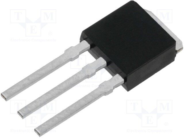
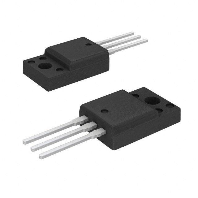
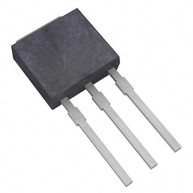
| 产品图片 |
|
| 产品型号 | STD4NK50Z-1 |
| rohs | 无铅 / 符合限制有害物质指令(RoHS)规范要求 |
| 产品系列 | SuperMESH™ |
| 不同Id时的Vgs(th)(最大值) | 4.5V @ 50µA |
| 不同Vds时的输入电容(Ciss) | 310pF @ 25V |
| 不同Vgs时的栅极电荷(Qg) | 12nC @ 10V |
| 不同 Id、Vgs时的 RdsOn(最大值) | 2.7 欧姆 @ 1.5A,10V |
| 供应商器件封装 | I-Pak |
| 其它名称 | 497-12559-5 |
| 其它有关文件 | http://www.st.com/web/catalog/sense_power/FM100/CL824/SC1167/PF223235?referrer=70071840 |
| 功率-最大值 | 45W |
| 包装 | 管件 |
| 安装类型 | 通孔 |
| 封装/外壳 | TO-251-3 长引线,IPak,TO-251AB |
| 标准包装 | 75 |
| 漏源极电压(Vdss) | 500V |
| 电流-连续漏极(Id)(25°C时) | 3A (Tc) |


PDF Datasheet 数据手册内容提取
STD4NK50Z-1, STD4NK50ZT4 Datasheet N-channel 500 V, 2.2 Ω typ., 3 A SuperMESH™ Power MOSFETs in IPAK and DPAK packages Features Order codes VDS RDS(on) max. PTOT Package TAB TAB STD4NK50Z-1 IPAK 23 500 V 2.7 Ω 45 W 3 1 STD4NK50ZT4 DPAK 2 IPAK 1 DPAK • Extremely high dv/dt capability • 100% avalanche tested • Gate charge minimized D(2, TAB) • Very low intrinsic capacitance • Zener-protected G(1) Applications • Switching applications S(3) Description AM01475V1 These high-voltage devices are Zener-protected N-channel Power MOSFETs developed using the SuperMESH™ technology by STMicroelectronics, an optimization of the well-established PowerMESH™. In addition to a significant reduction in on-resistance, these devices are designed to ensure a high level of dv/dt capability for the most demanding applications. Product status link STD4NK50Z-1 STD4NK50ZT4 DS2913 - Rev 3 - August 2018 www.st.com For further information contact your local STMicroelectronics sales office.
STD4NK50Z-1, STD4NK50ZT4 Electrical ratings 1 Electrical ratings Table 1. Absolute maximum ratings Symbol Parameter Value Unit VDS Drain-source voltage 500 V VGS Gate-source voltage ±30 V ID Drain current (continuous) at TC = 25 °C 3 A ID Drain current (continuous) at TC = 100 °C 1.9 A IDM (1) Drain current (pulsed) 12 A PTOT Total dissipation at TC = 25 °C 45 W dv/dt (2) Peak diode recovery voltage slope 4.5 V/ns ESD Gate-source human body model (C = 100 pF, R = 1.5 kΩ) 2.8 kV Tj Operating junction temperature range -55 to 150 °C Tstg Storage temperature range 1. Pulse width limited by safe operating area. 2. ISD ≤ 3 A, di/dt ≤ 200 A/µs, VDD ≤ V(BR)DSS. Table 2. Thermal data Symbol Parameter Value Unit IPAK DPAK Rthj-case Thermal resistance junction-case 2.78 °C/W Rthj-amb Thermal resistance junction-ambient 100 °C/W Rthj-pcb (1) Thermal resistance junction-pcb 50 °C/W 1. When mounted on an 1-inch² FR-4, 2oz Cu board. Table 3. Avalanche characteristics Symbol Parameter Value Unit Avalanche current, repetitive or not-repetitive IAR 3 A (pulse width limited by Tj max) Single pulse avalanche energy EAS 120 mJ (starting Tj = 25 °C, ID = IAR, VDD = 50 V) DS2913 - Rev 3 page 2/23
STD4NK50Z-1, STD4NK50ZT4 Electrical characteristics 2 Electrical characteristics (T = 25 °C unless otherwise specified) CASE Table 4. On/off states Symbol Parameter Test conditions Min. Typ. Max. Unit Drain-source breakdown V(BR)DSS voltage VGS = 0 V, ID = 1 mA 500 V VGS = 0 V, VDS = 500 V 1 µA Zero gate voltage drain IDSS current VGS = 0 V, VDS = 500 V, 50 µA TC = 125 °C (1) IGSS Gate-body leakage current VDS = 0 V, VGS = ±20 V ±10 µA VGS(th) Gate threshold voltage VDS = VGS, ID = 50 µA 3 3.75 4.5 V Static drain-source on RDS(on) resistance VGS = 10 V, ID = 1.5 A 2.2 2.7 Ω 1. Defined by design, not subject to production test. Table 5. Dynamic Symbol Parameter Test conditions Min. Typ. Max. Unit Ciss Input capacitance 310 VDS = 25 V, f = 1 MHz, Coss Output capacitance - 49 VGS = 0 V pF Crss Reverse transfer capacitance 10 Coss eq. (1) Equivalent output capacitance VGS = 0 V, VDS = 0 V to 400 V - 33 Qg Total gate charge VDD = 400 V, ID = 3 A, 12 Qgs Gate-source charge VGS = 0 to 10 V - 3 nC (see Figure 14. Test circuit for Qgd Gate-drain charge gate charge behavior) 7 1. Coss eq. is defined as a constant equivalent capacitance giving the same charging time as Coss when VDSincreases from 0 to 80% VDSS. Table 6. Switching times Symbol Parameter Test conditions Min. Typ. Max. Unit td(on) Turn-on delay time VDD = 250 V, ID = 1.5 A, 10 tr Rise time RG = 4.7 Ω, VGS = 10 V 7 td(off) Turn-off delay time (see Figure 13. Test circuit for - 21 ns resistive load switching times and Figure 18. Switching time tf Fall time waveform) 11 DS2913 - Rev 3 page 3/23
STD4NK50Z-1, STD4NK50ZT4 Electrical characteristics Table 7. Source-drain diode Symbol Parameter Test conditions Min. Typ. Max. Unit ISD Source-drain current - 3 A ISDM (1) Source-drain current (pulsed) - 12 VSD (2) Forward on voltage ISD = 3 A, VGS = 0 V - 1.6 V trr Reverse recovery time ISD = 3 A, di/dt = 100 A/µs - 260 ns Qrr Reverse recovery charge VDD = 40 V, Tj = 150 °C - 935 nC (see Figure 15. Test circuit for IRRM Reverse recovery current inductive load switching and - 7.2 A diode recovery times) 1. Pulse width limited by safe operating area. 2. Pulsed: Pulse duration = 300 μs, duty cycle 1.5 %. Table 8. Gate-source Zener diode Symbol Parameter Test conditions Min. Typ. Max. Unit Gate-source breakdown V(BR)GSO voltage IGS = ±1 mA, ID = 0 A ±30 - - V The built-in back-to-back Zener diodes are specifically designed to enhance the ESD performance of the device. The Zener voltage facilitates efficient and cost-effective device integrity protection, thus eliminating the need for additional external componentry. DS2913 - Rev 3 page 4/23
STD4NK50Z-1, STD4NK50ZT4 Electrical characteristics (curves) 2.1 Electrical characteristics (curves) Figure 1. Safe operating area Figure 2. Thermal impedance K GC20460 100 10-1 10-2 10-5 10-4 10-3 10-2 10-1 tp (s) Figure 3. Output characterisics Figure 4. Transfer characteristics Figure 5. Capacitance variations Figure 6. Gate charge vs gate-source voltage DS2913 - Rev 3 page 5/23
STD4NK50Z-1, STD4NK50ZT4 Electrical characteristics (curves) Figure 7. Normalized gate threshold voltage vs Figure 8. Static drain-source on resistance temperature Figure 9. Source-drain diode forward characteristic Figure 10. Maximum avalanche energy vs temperature Figure 11. Normalized V(BR)DSS vs temperature Figure 12. Normalized on resistance vs temperature DS2913 - Rev 3 page 6/23
STD4NK50Z-1, STD4NK50ZT4 Test circuits 3 Test circuits Figure 13. Test circuit for resistive load switching times Figure 14. Test circuit for gate charge behavior VDD 12 V 47 kΩ 1 kΩ 100 nF RL 2200 3.3 + μF μF VDD VD VGS IG= CONST 100 Ω D.U.T. VGS RG D.U.T. pulse width 2200+ 2.7 kΩ VG pulse width μF 47 kΩ 1 kΩ AM01468v1 AM01469v1 Figure 15. Test circuit for inductive load switching and Figure 16. Unclamped inductive load test circuit diode recovery times A A A L G DD.U.T. fdaiostde 100 µH VD 2200 3.3 25 Ω S B B B D µ3F.3 +1µ0F00 VDD ID +µF µF VDD G D.U.T. + RG S Vi D.U.T. _ pulse width AM01471v1 AM01470v1 Figure 18. Switching time waveform Figure 17. Unclamped inductive waveform ton toff V(BR)DSS td(on) tr td(off) tf VD 90% 90% IDM ID 0 10% VDS 10% VDD VDD VGS 90% 0 10% AM01472v1 AM01473v1 DS2913 - Rev 3 page 7/23
STD4NK50Z-1, STD4NK50ZT4 Package information 4 Package information In order to meet environmental requirements, ST offers these devices in different grades of ECOPACK® packages, depending on their level of environmental compliance. ECOPACK® specifications, grade definitions and product status are available at: www.st.com. ECOPACK® is an ST trademark. DS2913 - Rev 3 page 8/23
STD4NK50Z-1, STD4NK50ZT4 IPAK (TO-251) type A package information 4.1 IPAK (TO-251) type A package information Figure 19. IPAK (TO-251) type A package outline 0068771_IK_typeA_rev14 DS2913 - Rev 3 page 9/23
STD4NK50Z-1, STD4NK50ZT4 IPAK (TO-251) type A package information Table 9. IPAK (TO-251) type A package mechanical data mm Dim. Min. Typ. Max. A 2.20 2.40 A1 0.90 1.10 b 0.64 0.90 b2 0.95 b4 5.20 5.40 B5 0.30 c 0.45 0.60 c2 0.48 0.60 D 6.00 6.20 E 6.40 6.60 e 2.28 e1 4.40 4.60 H 16.10 L 9.00 9.40 L1 0.80 1.20 L2 0.80 1.00 V1 10° DS2913 - Rev 3 page 10/23
STD4NK50Z-1, STD4NK50ZT4 IPAK (TO-251) type C package information 4.2 IPAK (TO-251) type C package information Figure 20. IPAK (TO-251) type C package outline 0068771_IK_typeC_rev14 DS2913 - Rev 3 page 11/23
STD4NK50Z-1, STD4NK50ZT4 IPAK (TO-251) type C package information Table 10. IPAK (TO-251) type C package mechanical data mm Dim. Min. Typ. Max. A 2.20 2.30 2.35 A1 0.90 1.00 1.10 b 0.66 0.79 b2 0.90 b4 5.23 5.33 5.43 c 0.46 0.59 c2 0.46 0.59 D 6.00 6.10 6.20 D1 5.20 5.37 5.55 E 6.50 6.60 6.70 E1 4.60 4.78 4.95 e 2.20 2.25 2.30 e1 4.40 4.50 4.60 H 16.18 16.48 16.78 L 9.00 9.30 9.60 L1 0.80 1.00 1.20 L2 0.90 1.08 1.25 θ1 3° 5° 7° θ2 1° 3° 5° DS2913 - Rev 3 page 12/23
STD4NK50Z-1, STD4NK50ZT4 DPAK (TO-252) type A package information 4.3 DPAK (TO-252) type A package information Figure 21. DPAK (TO-252) type A package outline 0068772_A_25 DS2913 - Rev 3 page 13/23
STD4NK50Z-1, STD4NK50ZT4 DPAK (TO-252) type A package information Table 11. DPAK (TO-252) type A mechanical data mm Dim. Min. Typ. Max. A 2.20 2.40 A1 0.90 1.10 A2 0.03 0.23 b 0.64 0.90 b4 5.20 5.40 c 0.45 0.60 c2 0.48 0.60 D 6.00 6.20 D1 4.95 5.10 5.25 E 6.40 6.60 E1 4.60 4.70 4.80 e 2.159 2.286 2.413 e1 4.445 4.572 4.699 H 9.35 10.10 L 1.00 1.50 (L1) 2.60 2.80 3.00 L2 0.65 0.80 0.95 L4 0.60 1.00 R 0.20 V2 0° 8° DS2913 - Rev 3 page 14/23
STD4NK50Z-1, STD4NK50ZT4 DPAK (TO-252) type C package information 4.4 DPAK (TO-252) type C package information Figure 22. DPAK (TO-252) type C package outline 0068772_C_25 DS2913 - Rev 3 page 15/23
STD4NK50Z-1, STD4NK50ZT4 DPAK (TO-252) type C package information Table 12. DPAK (TO-252) type C mechanical data mm Dim. Min. Typ. Max. A 2.20 2.30 2.38 A1 0.90 1.01 1.10 A2 0.00 0.10 b 0.72 0.85 b4 5.13 5.33 5.46 c 0.47 0.60 c2 0.47 0.60 D 6.00 6.10 6.20 D1 5.25 E 6.50 6.60 6.70 E1 4.70 e 2.186 2.286 2.386 H 9.80 10.10 10.40 L 1.40 1.50 1.70 L1 2.90 REF L2 0.90 1.25 L3 0.51 BSC L4 0.60 0.80 1.00 L6 1.80 BSC θ1 5° 7° 9° θ2 5° 7° 9° V2 0° 8° DS2913 - Rev 3 page 16/23
STD4NK50Z-1, STD4NK50ZT4 DPAK (TO-252) type C package information Figure 23. DPAK (TO-252) recommended footprint (dimensions are in mm) FP_0068772_25_C DS2913 - Rev 3 page 17/23
STD4NK50Z-1, STD4NK50ZT4 DPAK (TO-252) packing information 4.5 DPAK (TO-252) packing information Figure 24. DPAK (TO-252) tape outline 10 pitches cumulative tolerance on tape +/- 0.2 mm Top cover P0 D P2 T tape E F K0 W B1 B0 For machine ref. only A0 P1 D1 including draft and radii concentric around B0 User direction of feed R Bending radius User direction of feed AM08852v1 DS2913 - Rev 3 page 18/23
STD4NK50Z-1, STD4NK50ZT4 DPAK (TO-252) packing information Figure 25. DPAK (TO-252) reel outline T 40mm min. access hole at slot location B D C N A Tape slot G measured in core for at hub Full radius tape start 2.5mm min.width AM06038v1 Table 13. DPAK (TO-252) tape and reel mechanical data Tape Reel mm mm Dim. Dim. Min. Max. Min. Max. A0 6.8 7 A 330 B0 10.4 10.6 B 1.5 B1 12.1 C 12.8 13.2 D 1.5 1.6 D 20.2 D1 1.5 G 16.4 18.4 E 1.65 1.85 N 50 F 7.4 7.6 T 22.4 K0 2.55 2.75 P0 3.9 4.1 Base qty. 2500 P1 7.9 8.1 Bulk qty. 2500 P2 1.9 2.1 R 40 T 0.25 0.35 W 15.7 16.3 DS2913 - Rev 3 page 19/23
STD4NK50Z-1, STD4NK50ZT4 Ordering information 5 Ordering information Table 14. Order codes Order code Marking Package Packing STD4NK50Z-1 IPAK Tube D4NK50Z STD4NK50ZT4 DPAK Tape and reel DS2913 - Rev 3 page 20/23
STD4NK50Z-1, STD4NK50ZT4 Revision history Table 15. Document revision history Date Version Changes 09-Dec-2002 2 Updated document. Removed maturity status indication from cover page. The document status is production data. The part numbers STP4NK50Z and STP4NK50FP have been moved to a separate datasheet. 20-Aug-2018 3 Updated Section 1 Electrical ratings, Section 2 Electrical characteristics and Section 4 Package information. Added Section 5 Ordering information. Minor text changes. DS2913 - Rev 3 page 21/23
STD4NK50Z-1, STD4NK50ZT4 Contents Contents 1 Electrical ratings ..................................................................2 2 Electrical characteristics...........................................................3 2.1 Electrical characteristics (curves) .................................................5 3 Test circuits .......................................................................7 4 Package information...............................................................8 4.1 IPAK (TO-251) type A package information.........................................8 4.2 IPAK (TO-251) type C package information........................................10 4.3 DPAK (TO-252) type A package information.......................................12 4.4 DPAK (TO-252) type C package information.......................................14 4.5 DPAK (TO-252) packing information..............................................17 5 Ordering information .............................................................20 Revision history .......................................................................21 DS2913 - Rev 3 page 22/23
STD4NK50Z-1, STD4NK50ZT4 IMPORTANT NOTICE – PLEASE READ CAREFULLY STMicroelectronics NV and its subsidiaries (“ST”) reserve the right to make changes, corrections, enhancements, modifications, and improvements to ST products and/or to this document at any time without notice. Purchasers should obtain the latest relevant information on ST products before placing orders. ST products are sold pursuant to ST’s terms and conditions of sale in place at the time of order acknowledgement. Purchasers are solely responsible for the choice, selection, and use of ST products and ST assumes no liability for application assistance or the design of Purchasers’ products. No license, express or implied, to any intellectual property right is granted by ST herein. Resale of ST products with provisions different from the information set forth herein shall void any warranty granted by ST for such product. ST and the ST logo are trademarks of ST. All other product or service names are the property of their respective owners. Information in this document supersedes and replaces information previously supplied in any prior versions of this document. © 2018 STMicroelectronics – All rights reserved DS2913 - Rev 3 page 23/23