ICGOO在线商城 > 分立半导体产品 > 晶体管 - 双极 (BJT) - 阵列 > MAT01AH
 Datasheet下载
- 型号: MAT01AH
- 制造商: Analog
- 库位|库存: xxxx|xxxx
- 要求:
| 数量阶梯 | 香港交货 | 国内含税 |
| +xxxx | $xxxx | ¥xxxx |
查看当月历史价格
查看今年历史价格
MAT01AH产品简介:
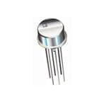
ICGOO电子元器件商城为您提供MAT01AH由Analog设计生产,在icgoo商城现货销售,并且可以通过原厂、代理商等渠道进行代购。 MAT01AH价格参考¥182.87-¥211.00。AnalogMAT01AH封装/规格:晶体管 - 双极 (BJT) - 阵列, Bipolar (BJT) Transistor Array 2 NPN (Dual) Matched Pair 45V 25mA 450MHz 500mW Through Hole TO-78-6。您可以下载MAT01AH参考资料、Datasheet数据手册功能说明书,资料中有MAT01AH 详细功能的应用电路图电压和使用方法及教程。
MAT01AH 是由 Analog Devices Inc. 生产的一款双极型晶体管 (BJT) 阵列,其应用场景广泛,尤其适用于需要高精度、低噪声和高性能的电路设计。以下是 MAT01AH 的主要应用场景:

1. 运算放大器输入级
   MAT01AH 的高匹配特性和低基极-发射极电压偏差使其非常适合用于构建运算放大器的输入差分对。这种应用可以显著提高运放的共模抑制比 (CMRR) 和增益精度。

2. 模拟信号处理
   在音频设备、传感器信号调理和数据采集系统中,MAT01AH 可用于实现高精度的信号放大和处理。其低噪声和高线性度特性能够确保信号不失真。

3. 电流镜和有源负载
   由于 MAT01AH 内部晶体管的高度匹配,它非常适合用作电流镜或有源负载,从而在精密电源管理和放大器设计中提供稳定的电流输出。

4. 温度补偿电路
   MAT01AH 的晶体管阵列具有良好的热耦合性能,这使得它在温度敏感的应用中表现出色,例如温度补偿放大器或精密基准源。

5. 高速开关和脉冲电路
   MAT01AH 的快速开关特性和低饱和压降使其适合用于高速数字电路中的开关应用,如驱动器或脉冲发生器。

6. 测试与测量设备
   在精密仪器和测试设备中,MAT01AH 可用于实现高精度的信号放大和处理,满足对分辨率和稳定性的严格要求。

7. 通信系统
   在射频 (RF) 和中频 (IF) 电路中,MAT01AH 的低噪声和高增益特性可用于前端放大器和混频器设计。

总结来说,MAT01AH 凭借其高匹配度、低噪声和优异的电气性能,广泛应用于精密放大、信号处理、电源管理以及测试测量等领域。这些特性使其成为许多高性能模拟电路设计的理想选择。
| 参数 | 数值 |
| 产品目录 | |
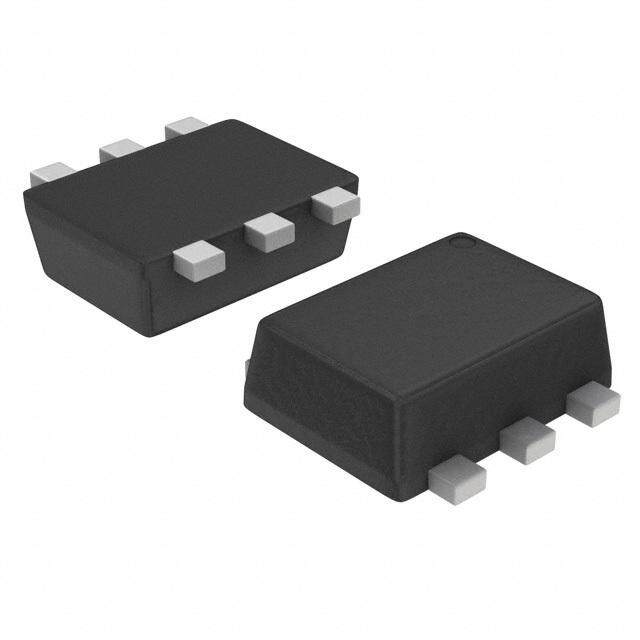
| 描述 | TRANS DUAL NPN 45V 25MA TO78-6 |
| 产品分类 | 晶体管(BJT) - 阵列 |
| 品牌 | Analog Devices Inc |
| 数据手册 | |
| 产品图片 |
|
| 产品型号 | MAT01AH |
| rohs | 含铅 / 不符合限制有害物质指令(RoHS)规范要求 |
| 产品系列 | - |
| 不同 Ib、Ic时的 Vce饱和值(最大值) | 800mV @ 1mA,10mA |
| 不同 Ic、Vce 时的DC电流增益(hFE)(最小值) | - |
| 供应商器件封装 | TO-78-6 |
| 功率-最大值 | 500mW |
| 包装 | 管件 |
| 安装类型 | 通孔 |
| 封装/外壳 | TO-78-6 金属罐 |
| 晶体管类型 | 2 NPN(双)配对 |
| 标准包装 | 1 |
| 电压-集射极击穿(最大值) | 45V |
| 电流-集电极(Ic)(最大值) | 25mA |
| 电流-集电极截止(最大值) | 300nA |
| 频率-跃迁 | 450MHz |


- 商务部:美国ITC正式对集成电路等产品启动337调查
- 曝三星4nm工艺存在良率问题 高通将骁龙8 Gen1或转产台积电
- 太阳诱电将投资9.5亿元在常州建新厂生产MLCC 预计2023年完工
- 英特尔发布欧洲新工厂建设计划 深化IDM 2.0 战略
- 台积电先进制程称霸业界 有大客户加持明年业绩稳了
- 达到5530亿美元!SIA预计今年全球半导体销售额将创下新高
- 英特尔拟将自动驾驶子公司Mobileye上市 估值或超500亿美元
- 三星加码芯片和SET,合并消费电子和移动部门,撤换高东真等 CEO
- 三星电子宣布重大人事变动 还合并消费电子和移动部门
- 海关总署:前11个月进口集成电路产品价值2.52万亿元 增长14.8%


PDF Datasheet 数据手册内容提取
Matched Monolithic Dual Transistor Data Sheet MAT01 FEATURES PIN CONNECTION DIAGRAM Low V (V match): 40 µV typical, 100 µV maximum MAT01 OS BE TOP VIEW Low TCVOS: 0.5 µV/°C maximum (Not to Scale) High h : 500 minimum FE Excellent h linearity from 10 nA to 10 mA C1 1 6 C2 FE Low noise voltage: 0.23 µV p-p from 0.1 Hz to 10 Hz High breakdown: 45 V min B1 2 5 B2 APPLICATIONS E1 3 4 E2 WLoewig nho siscea,l eosp amp, front end N1.O STUEBSSTRATE IS CONNECTEDTO CASE. 00282-001 Current mirror and current sink/source Figure 1. Low noise instrumentation amplifiers Voltage controlled attenuators Log amplifiers GENERAL DESCRIPTION The MAT01 is a monolithic dual NPN transistor. An exclusive High h is provided over a six decade range of collector FE silicon nitride triple passivation process provides excellent current, including an exceptional h of 590 at a collector FE stability of critical parameters over both temperature and time. current of only 10 nA. The high gain at low collector current Matching characteristics include offset voltage of 40 µV, makes the MAT01 ideal for use in low power, low level input temperature drift of 0.15 µV/°C, and h matching of 0.7%. stages. FE Rev. D Document Feedback Information furnished by Analog Devices is believed to be accurate and reliable. However, no responsibility is assumed by Analog Devices for its use, nor for any infringements of patents or other One Technology Way, P.O. Box 9106, Norwood, MA 02062-9106, U.S.A. rights of third parties that may result from its use. Specifications subject to change without notice. No license is granted by implication or otherwise under any patent or patent rights of Analog Devices. Tel: 781.329.4700 ©1973–2014 Analog Devices, Inc. All rights reserved. Trademarks and registered trademarks are the property of their respective owners. Technical Support www.analog.com
MAT01 Data Sheet TABLE OF CONTENTS Features .............................................................................................. 1 ESD Caution...................................................................................5 Applications ....................................................................................... 1 Typical Performance Characteristics ..............................................6 Pin Connection Diagram ................................................................ 1 Test Circuits ........................................................................................8 General Description ......................................................................... 1 Applications Information .................................................................9 Revision History ............................................................................... 2 Typical Applications ....................................................................... 10 Specifications ..................................................................................... 3 Outline Dimensions ....................................................................... 11 Electrical Characteristics ............................................................. 3 Ordering Guide .......................................................................... 11 Absolute Maximum Ratings ............................................................ 5 REVISION HISTORY 9/14—Rev. C to Rev. D 2/02—Rev. A to Rev. B Changes to Figure 4 and Figure 7 ................................................... 6 Edits to Features................................................................................. 1 Deleted Wafer Test Limits ................................................................ 3 4/13—Rev. B to Rev. C Deleted DICE Characteristics .......................................................... 3 Updated Format .................................................................. Universal Edits to Table 5 ................................................................................... 7 Added Applications Section, Deleted Figure 2, Renumbered Sequentially ................................................................ 1 Deleted Table 3, Renumbered Sequentially................................... 4 Changes to Table 3 ............................................................................ 5 Changes to Typical Performance Characteristics Section ........... 6 Updated Outline Dimensions ....................................................... 11 Changes to Ordering Guide .......................................................... 11 Rev. D | Page 2 of 12
Data Sheet MAT01 SPECIFICATIONS ELECTRICAL CHARACTERISTICS V = 15 V, I = 10 µA, T = 25°C, unless otherwise noted. CB C A Table 1. MAT01AH MAT01GH Parameter Symbol Test Conditions/Comments Min Typ Max Min Typ Min Unit VOLTAGE Breakdown Voltage BV I = 100 µA 45 45 V CEO C Offset Voltage V 0.04 0.1 0.10 0.5 mV OS Offset Voltage Stability First Month1 V /Time 2.0 2.0 µV/Mo OS Long Term2 0.2 0.2 µV/Mo CURRENT Offset Current I 0.1 0.6 0.2 3.2 nA OS Bias Current I 13 20 18 40 nA B Current Gain h I = 10 nA 590 430 FE C I = 10 µA 500 770 250 560 C I = 10 mA 840 610 C Current Gain Match ∆h I = 10 µA 0.7 3.0 1.0 8.0 % FE C 100 nA ≤ I ≤ 10 mA 0.8 1.2 % C NOISE Low Frequency Noise Voltage e p-p 0.1 Hz to 10 Hz3 0.23 0.4 0.23 0.4 µV p-p n Broadband Noise Voltage e rms 1 Hz to 10 kHz 0.60 0.60 µV rms n Noise Voltage Density e f = 10 Hz3 7.0 9.0 7.0 9.0 nV/√Hz n O f = 100 Hz3 6.1 7.6 6.1 7.6 nV/√Hz O f = 1000 Hz3 6.0 7.5 6.0 7.5 nV/√Hz O OFFSET VOLTAGE/CURRENT Offset Voltage Change ∆V /∆V 0 ≤ V ≤ 30 V 0.5 3.0 0.8 8.0 µV/V OS CB CB Offset Current Change ∆I /∆V 0 ≤ V ≤ 30 V 2 15 3 70 pA/V OS CB CB LEAKAGE Collector to Base Leakage Current I V = 30 V, I = 04 15 50 25 200 pA CBO CB E Collector to Emitter Leakage Current I V = 30 V, V = 04, 5 50 200 90 400 pA CES CE BE Collector to Collector Leakage Current I V = 30 V5 20 200 30 400 pA CC CC SATURATION Collector Saturation Voltage V I = 0.1 mA, I = 1 mA 0.12 0.20 0.12 0.25 V CE(SAT) B C I = 1 mA, I = 10 mA 0.8 0.8 V B C GAIN BANDWIDTH PRODUCT f V = 10 V, I = 10 mA 450 450 MHz T CE C CAPACITANCE Output Capacitance C V = 15 V, I = 0 2.8 2.8 pF OB CB E Collector to Collector Capacitance C V = 0 8.5 8.5 pF CC CC 1 Exclude first hour of operation to allow for stabilization. 2 Parameter describes long-term average drift after first month of operation. 3 Sample tested. 4 The collector to base (ICBO) and collector to emitter (ICES) leakage currents can be reduced by a factor of 2 to 10 times by connecting the substrate (package) to a potential that is lower than either collector voltage. 5 ICC and ICES are guaranteed by measurement of ICBO. Rev. D | Page 3 of 12
MAT01 Data Sheet V = 15 V, I = 10 µA, −55°C ≤ T ≤ +125°C, unless otherwise noted. CB C A Table 2. MAT01AH MAT01GH Parameter Symbol Test Conditions/Comments Min Typ Max Min Typ Min Unit OFFSET VOLTAGE/CURRENT Offset Voltage V 0.06 0.15 0.14 0.70 mV OS Average Offset Voltage Drift1 TCV 0.15 0.50 0.35 1.8 µV/°C OS Offset Current I 0.9 8.0 1.5 15.0 nA OS Average Offset Current Drift2 TCI 10 90 15 150 pA/°C OS BIAS CURRENT Ι 28 60 36 130 nA Β CURRENT GAIN h 167 400 77 300 FE LEAKAGE CURRENT Collector to Base Leakage Current I T = 125°C, V = 30 V, I = 03 15 80 25 200 nA CBO A CB E Collector to Emitter Leakage Current I T = 125°C, V = 30 V, V = 01, 3 50 300 90 400 nA CES A CE BE Collector to Collector Leakage Current I T = 125°C, V = 30 V1 30 200 50 400 nA CC A CC ( ) V 1 Guaranteed by VOS test TCVOS≅ OTSforVOS<<VBE , T = 298 K for TA = 25°C. 2 Guaranteed by IOS test limits over temperature. 3 The collector to base (ICBO) and collector to emitter (ICES) leakage currents can be reduced by a factor of 2 to 10 times by connecting the substrate (package) to a potential that is lower than either collector voltage. Rev. D | Page 4 of 12
Data Sheet MAT01 ABSOLUTE MAXIMUM RATINGS Stresses above those listed under Absolute Maximum Ratings Table 3. may cause permanent damage to the device. This is a stress Parameter1 Rating rating only; functional operation of the device at these or any Breakdown Voltage of other conditions above those indicated in the operational Collector to Base Voltage (BV ) 45 V CBO section of this specification is not implied. Exposure to absolute Collector to Emitter Voltage (BV ) 45 V CEO maximum rating conditions for extended periods may affect Collector to Collector Voltage (BV ) 45 V CC device reliability. Emitter to Emitter Voltage (BV ) 45 V EE Emitter to Base Voltage (BV )2 5 V EBO Current ESD CAUTION Collector (I ) 25 mA C Emitter (I) 25 mA E Total Power Dissipation Case Temperature ≤ 40°C3 1.8 W Ambient Temperature ≤ 70°C4 500 mW Temperature Range Operating −55°C to +125°C Junction −55°C to +150°C Storage −65°C to +150°C Lead Temperature (Soldering, 60 sec) 300°C 1 Absolute maximum ratings apply to packaged devices. 2 Application of reverse bias voltages in excess of rating shown can result in degradation of hFE and hFE matching characteristics. Do not attempt to measure BVEBO greater than the 5 V rating. 3 Rating applies to applications using heat sinking to control case temperature. Derate linearity at 16.4 mW/°C for case temperatures above 40°C. 4 Rating applies to applications not using heat sinking; device in free air only. Derate linearity at 6.3 mW/°C for ambient temperatures above 70°C. Rev. D | Page 5 of 12
MAT01 Data Sheet TYPICAL PERFORMANCE CHARACTERISTICS 200 V) 10 OV < VCB < 30V E (µ 8 G A T 6 L LTAGE (µV) 150 MAT01G OFFSET VO 42 DDEEVVICICEE B A SET VO 100 NGE IN –20 DEVICE C F A DEVICE D OF MAT01A CH –4 50 E UT –6 L 0 00282-002 ABSO –1–08 00282-005 –75 –25 0 25 50 75 100 125 150 0 1 2 3 4 5 6 7 8 9 10 11 12 13 TEMPERATURE (°C) TIME (Months) Figure 2. Offset Voltage vs. Temperature Figure 5. Offset Voltage vs. Time 1000 1000 MAT01A MAT01A 800 800 h)FE MAT01G h)fe N ( 600 N ( MAT01G AI AI G G NT NT 600 RE 400 RE R R U U C C 400 200 100nA < IC < 25mA 0 VTAC B= =2 51°5CV 00282-003 200 O(EVX C< LVUCDBE <S 3 I0CVBO) 00282-006 1n 10n 100n 1µ 10µ 100µ 1m 10m 100m –75 –50 –25 0 25 50 75 100 125 COLLECTOR CURRENT (A) TEMPERATURE (°C) Figure 3. Current Gain vs. Collector Current Figure 6. Current Gain vs. Temperature 1000 100 TA = 25°C TA = 25°C Hz) Hz) √ √ V/ A/ n p TY ( 100 TY ( 10 SI SI N N E E D D TAGE RENT WOICR =S T1 0CµAASE IC = 300µA TYPICAL L R VO 10 IC = 10µA WORST CASE CU 1 E E NOIS IC = 10µA TYPICAL NOIS IC = 10µA TYPICAL 1 IC = 300µA TYPICAL 00282-004 0.1 00282-007 0.1 1 10 100 10k 10k 0.1 1 10 100 1k 10k FREQUENCY (Hz) FREQUENCY (Hz) Figure 4. Noise Voltage Density vs. Frequency Figure 7. Noise Current Density vs. Frequency Rev. D | Page 6 of 12
Data Sheet MAT01 10mA 1000 1mA MAT01 Hz) 500 TA = 25°C M ENT (I)C10100µµAA Δ < 0.3mV RODUCT ( 120000 TVAC E= =2 51°0CV R P MAT01 R H U 1µA T 50 R C Δ < 0.1mV WID O100nA D 20 LLECT 10nA N BAN 10 CO 1nA Y-GAI 5 10100ppAA Δ < 0.3mV Δ ≈S DTERVAIIAGTHIOT NL IFNREOM 00282-008 UNIT 12 00282-010 0 100 200 300 400 500 600 700 800 1µA 10µA 100µA 1mA 10mA 100mA BASE TO EMITTER VOLTAGE (mV) COLLECTOR CURRENT (IC) Figure 8. Collector Current vs. Base to Emitter Voltage Figure 10. Unity-Gain Bandwidth vs. Collector Current 100 MAT01 IC = 10 × IB GE (V) 10 TA = +125°C A T L O V ON 1 TA = +25°C TI A R TU TA = –55°C A S 0.1 0.01 00282-009 0.01 0.1 1 10 100 COLLECTOR CURRENT (mA) Figure 9. Saturation Voltage vs. Collector Current Rev. D | Page 7 of 12
MAT01 Data Sheet TEST CIRCUITS +16.5V +16.5V 50kΩ* 20kΩ 50kΩ* 50kΩ* VOUT OP1177 –15V TEST S1A S1B UNITS S1A S1B 110%0kΩ VOS CLOSEDCLOSED VOUT1 1V PER mV 1MΩ 1MΩ* IOS OPEN OPEN VOUT2 – VOUT1 1V PER nA MAT01 100pF 100pF 100kΩ 1% 20µA *MATCHEDTO 0.01% V– 00282-011 Figure 11. Matching Measurement Circuit +15V 50kΩ* SPECTRUM ANALYZER +15V OR 50kΩ* 50kΩ* QUAN-TECH V01 S3 B AINCA NLOYIZSEER NDEONISSEITY 2181/2283 A S2 3.3kΩ S1A S1B –15V 2.5MΩ LOW V02 FREQUENCY NOISE 4MΩ MAT01 4MΩ 4kΩ 4.7µF 2pF 2pF 100Ω 720kΩ 20µA –15V *MATCHEDTO 0.01% TEST S1A S1B S2 S3** READING NOI(SPEE RV OTLRTAANGSEIS DTEONRS)ITY CLOSED CLOSED CLOSED A V01/√2 NOI(SPEE RC UTRRRAENNSTIS DTEONRS)ITY OPEN OPEN CLOSED A V01/(√2 × 4MΩ) **LA(ORAWENF DFE RBRE RRQEEUDFEETNROC TYINO NP TOUHITSE)E THRCOLOWS PEODSICTLIOONS EODF THOEP SEWNITCHB V02PEA25K,0-T0O0-PEAK 00282-012 Figure 12. Noise Measurement Circuit Rev. D | Page 8 of 12
Data Sheet MAT01 APPLICATIONS INFORMATION Application of reverse bias voltages to the emitter to base junctions Stray thermoelectric voltages generated by dissimilar metals at in excess of ratings (5 V) may result in degradation of h and the contacts to the input terminals can prevent realization of the FE h matching characteristics. Check circuit designs to ensure predicted drift performance. Maintain both input terminals at FE that reverse bias voltages above 5 V cannot be applied during the same temperature, preferably close to the temperature of the transient conditions, such as at circuit turn-on and turn-off. device package. Rev. D | Page 9 of 12
MAT01 Data Sheet TYPICAL APPLICATIONS 1mA VREF Q1 Q2 R1 1.5kΩ VREF ≈ 7.0V TCVREF ≈ 100ppm/°C RO≈40Ω NOTES 12 .. hRINF1CE MR OAEFYA QSBI1EN IGASD RRJ1EU DCSUATCEUEDSDET SBO YA M OPINOPIESMRIITZAIEVT EITO CCNVH ORAEFNF GB.REE INA KTDCOVRWENF. MODE. 00282-013 Figure 13. Precision Reference UPTO 100 FEET +15V –15V CABLE DIFFERENTIAL EO = 10mV/K SENSINGPAIR AMPLIFIERAND MAT01H CURRENT SOURCES °C K EO –55°C = 218K = 2.18V +25°C = 298K = 2.98V 3-DIGIT DPM +125°C = 398K = 3.98V F0UVLTLO S C+1A0LVE 00282-014 Figure 14. Basic Digital Thermometer Readout in Degrees Kelvin (K) UPTO 100FT. +15V –15V CABLE DIFFERENTIAL EO = 10mV/K SENSINGPAIR AMPLIFIERAND MAT01H CURRENT SOURCES HIGH 2 1/2 DIGIT DPM BIPOLAR DIFFERENTIAL 2.73V + LOW INPUTS POWER SUPPLY – MEOE T–E2.R7 3DVISPLAYS + 1–+252555°°°CCC === +–+010...522555VVV 00282-015 Figure 15. Digital Thermometer with Readout in °C Rev. D | Page 10 of 12
Data Sheet MAT01 OUTLINE DIMENSIONS REFERENCE PLANE 0.750 (19.05) 0.185 (4.70) 0.500 (12.70) 0.165 (4.19) 0.250 (6.35) MIN 0.100 (2.54) BSC 0.050 (1.27) MAX 0.160 (4.06) 0.110 (2.79) 4 0.370 (9.40)0.335 (8.51) 0.335 (8.51)0.305 (7.75) (0B5..2S00C80) 32 5 6 00..004257 ((10..1649)) 0.019 (0.48) 0.100 1 (2.54) 0.040 (1.02) MAX 0.016 (0.41) BSC 0.034 (0.86) 0.021 (0.53) 0.027 (0.69) 0.045 (1.14) 0.016 (0.41) 45° 0.010 (0.25) BSC BASE & SEATING PLANE C(RINOEFNPETARRREOENNLCLTEIHN EOGSN EDLSIYM)AEANNRDSEI AORRNOESU NANORDEET DAIN-PO IPFNRFCO HINPECRSHI;A METEQIL UFLIOIVMRAE LUTEESNRET DISNI M FDOEERNSSIGIONN.S 022306-A Figure 16. 6-Pin Metal Header Package [TO-78] (H-06) Dimensions shown in inches and (millimeters) ORDERING GUIDE Model1 V Maximum (T = 25°C) Temperature Range Package Description Package Option OS A MAT01AH 0.1 mV −55°C to +125°C 6-Pin Metal Header Package [TO-78] H-06 MAT01AHZ 0.1 mV −55°C to +125°C 6-Pin Metal Header Package [TO-78] H-06 MAT01GH 0.5 mV −55°C to +125°C 6-Pin Metal Header Package [TO-78] H-06 MAT01GHZ 0.5 mV −55°C to +125°C 6-Pin Metal Header Package [TO-78] H-06 1 Z = RoHS Compliant Part. Rev. D | Page 11 of 12
MAT01 Data Sheet NOTES ©1973–2014 Analog Devices, Inc. All rights reserved. Trademarks and registered trademarks are the property of their respective owners. D00282-0-9/14(D) Rev. D | Page 12 of 12
Mouser Electronics Authorized Distributor Click to View Pricing, Inventory, Delivery & Lifecycle Information: A nalog Devices Inc.: MAT01AH MAT01GHZ MAT01AHZ MAT01GH