ICGOO在线商城 > 分立半导体产品 > 晶体管 - 双极 (BJT) - 阵列 > ULN2803ADWR
 Datasheet下载
- 型号: ULN2803ADWR
- 制造商: Texas Instruments
- 库位|库存: xxxx|xxxx
- 要求:
| 数量阶梯 | 香港交货 | 国内含税 |
| +xxxx | $xxxx | ¥xxxx |
查看当月历史价格
查看今年历史价格
ULN2803ADWR产品简介:
ICGOO电子元器件商城为您提供ULN2803ADWR由Texas Instruments设计生产,在icgoo商城现货销售,并且可以通过原厂、代理商等渠道进行代购。 ULN2803ADWR价格参考¥2.01-¥2.51。Texas InstrumentsULN2803ADWR封装/规格:晶体管 - 双极 (BJT) - 阵列, Bipolar (BJT) Transistor Array 8 NPN Darlington 50V 500mA Surface Mount 18-SOIC。您可以下载ULN2803ADWR参考资料、Datasheet数据手册功能说明书,资料中有ULN2803ADWR 详细功能的应用电路图电压和使用方法及教程。
ULN2803ADWR是Texas Instruments推出的一款高电压、大电流达林顿晶体管阵列,内部集成了8个NPN达林顿对管,每个通道可承受最高50V的负载电压和500mA的持续电流。该器件广泛应用于需要驱动较高功率负载的数字控制场景。

典型应用场景包括:工业控制中的继电器、电磁阀、步进电机等执行元件的驱动;打印机、扫描仪、数控设备等办公自动化和工业自动化设备中的电机控制;LED点阵显示屏或多路LED指示灯的动态扫描驱动;以及各类微控制器(如单片机、DSP、FPGA)与外围大电流负载之间的接口缓冲与电平转换。

ULN2803ADWR内置续流二极管,可有效抑制感性负载断电时产生的反向电动势,保护驱动电路,特别适合驱动继电器、电机等感性负载。其输入端兼容TTL和5V CMOS电平,便于与各类逻辑电路直接连接,无需额外电平转换。

由于采用SOIC-18封装,ULN2803ADWR体积小巧,适合高密度PCB布局,广泛用于空间受限但需多路驱动能力的应用中。凭借高可靠性与稳定性,该器件在工业、消费电子及汽车电子辅助系统中均有广泛应用。
| 参数 | 数值 |
| 产品目录 | |
| 描述 | TRANS 8 NPN DARL 50V 500MA 18SO达林顿晶体管 TRANSISTOR ARRAYS |
| 产品分类 | 晶体管(BJT) - 阵列分离式半导体 |
| 品牌 | Texas Instruments |
| 产品手册 | |
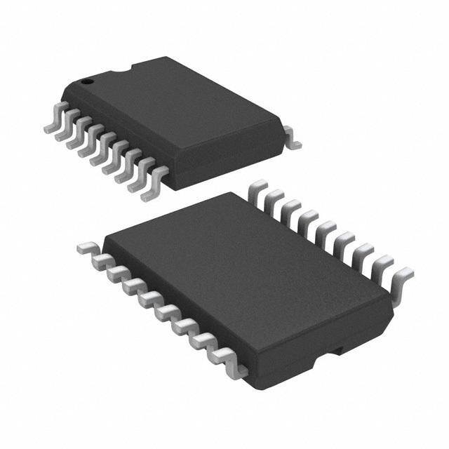
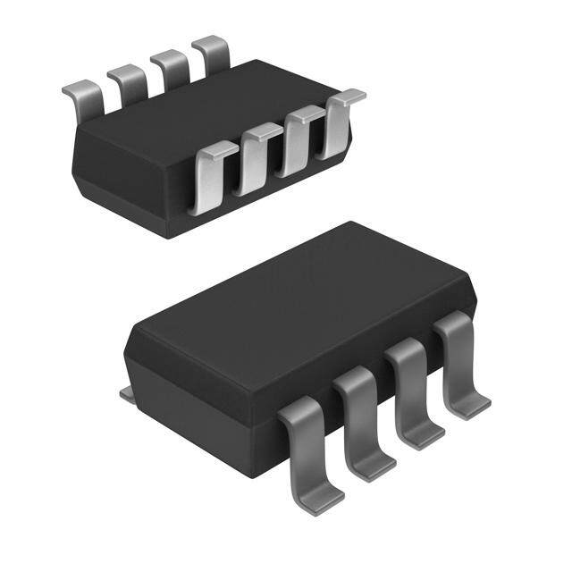
| 产品图片 |
|
| rohs | 符合RoHS无铅 / 符合限制有害物质指令(RoHS)规范要求 |
| 产品系列 | 晶体管,达林顿晶体管,Texas Instruments ULN2803ADWR- |
| 数据手册 | |
| 产品型号 | ULN2803ADWR |
| 不同 Ib、Ic时的 Vce饱和值(最大值) | 1.6V @ 500µA, 350mA |
| 不同 Ic、Vce 时的DC电流增益(hFE)(最小值) | - |
| 产品目录页面 | |
| 产品种类 | |
| 供应商器件封装 | 18-SOIC |
| 其它名称 | 296-15777-1 |
| 功率-最大值 | - |
| 包装 | 剪切带 (CT) |
| 商标 | Texas Instruments |
| 安装类型 | 表面贴装 |
| 安装风格 | SMD/SMT |
| 封装 | Reel |
| 封装/外壳 | 18-SOIC(0.295",7.50mm 宽) |
| 封装/箱体 | SOIC-18 |
| 工厂包装数量 | 2000 |
| 晶体管极性 | NPN |
| 晶体管类型 | 8 NPN 达林顿 |
| 最大工作温度 | + 150 C |
| 最大直流电集电极电流 | 0.5 A |
| 最小工作温度 | - 65 C |
| 标准包装 | 1 |
| 电压-集射极击穿(最大值) | 50V |
| 电流-集电极(Ic)(最大值) | 500mA |
| 电流-集电极截止(最大值) | - |
| 系列 | ULN2803A |
| 配置 | Octal |
| 集电极—发射极最大电压VCEO | 50 V |
| 频率-跃迁 | - |


- 商务部:美国ITC正式对集成电路等产品启动337调查
- 曝三星4nm工艺存在良率问题 高通将骁龙8 Gen1或转产台积电
- 太阳诱电将投资9.5亿元在常州建新厂生产MLCC 预计2023年完工
- 英特尔发布欧洲新工厂建设计划 深化IDM 2.0 战略
- 台积电先进制程称霸业界 有大客户加持明年业绩稳了
- 达到5530亿美元!SIA预计今年全球半导体销售额将创下新高
- 英特尔拟将自动驾驶子公司Mobileye上市 估值或超500亿美元
- 三星加码芯片和SET,合并消费电子和移动部门,撤换高东真等 CEO
- 三星电子宣布重大人事变动 还合并消费电子和移动部门
- 海关总署:前11个月进口集成电路产品价值2.52万亿元 增长14.8%


PDF Datasheet 数据手册内容提取
Product Order Technical Tools & Support & Folder Now Documents Software Community ULN2803A SLRS049H–FEBRUARY1997–REVISEDFEBRUARY2017 ULN2803A Darlington Transistor Arrays 1 Features 3 Description • 500-mA-RatedCollectorCurrent The ULN2803A device is a 50 V, 500 mA Darlington 1 transistor array. The device consists of eight NPN (SingleOutput) Darlington pairs that feature high-voltage outputs with • High-VoltageOutputs:50V common-cathode clamp diodes for switching • OutputClampDiodes inductive loads. The collector-current rating of each • InputsCompatibleWithVariousTypesofLogic Darlington pair is 500 mA. The Darlington pairs may beconnectedinparallelforhighercurrentcapability. 2 Applications Applications include relay drivers, hammer drivers, lamp drivers, display drivers (LED and gas • RelayDrivers discharge), line drivers, and logic buffers. The • HammerDrivers ULN2803A device has a 2.7-kΩ series base resistor • LampDrivers for each Darlington pair for operation directly with • DisplayDrivers(LEDandGasDischarge) TTLor5-VCMOSdevices. • LineDrivers DeviceInformation(1) • LogicBuffers PARTNUMBER PACKAGE BODYSIZE(NOM) • StepperMotors ULN2803ADW SOIC(18) 11.55mm×7.50mm • IPCamera (1) For all available packages, see the orderable addendum at • HVACValveandLEDDotMatrix theendofthedatasheet. LogicDiagram 1 18 1B 1C 2 17 2B 2C 3 16 3B 3C 4 15 4B 4C 5 14 5B 5C 6 13 6B 6C 7 12 7B 7C 8 11 8B 8C 10 COM 1 An IMPORTANT NOTICE at the end of this data sheet addresses availability, warranty, changes, use in safety-critical applications, intellectualpropertymattersandotherimportantdisclaimers.PRODUCTIONDATA.
ULN2803A SLRS049H–FEBRUARY1997–REVISEDFEBRUARY2017 www.ti.com Table of Contents 1 Features.................................................................. 1 8.3 FeatureDescription...................................................9 2 Applications........................................................... 1 8.4 DeviceFunctionalModes..........................................9 3 Description............................................................. 1 9 ApplicationandImplementation........................ 10 4 RevisionHistory..................................................... 2 9.1 ApplicationInformation............................................10 9.2 TypicalApplication .................................................10 5 PinConfigurationandFunctions......................... 3 10 PowerSupplyRecommendations..................... 12 6 Specifications......................................................... 4 11 Layout................................................................... 12 6.1 AbsoluteMaximumRatings......................................4 6.2 ESDRatings..............................................................4 11.1 LayoutGuidelines.................................................12 6.3 RecommendedOperatingConditions.......................4 11.2 LayoutExample....................................................12 6.4 ThermalInformation..................................................4 12 DeviceandDocumentationSupport................. 13 6.5 ElectricalCharacteristics...........................................5 12.1 ReceivingNotificationofDocumentationUpdates13 6.6 SwitchingCharacteristics..........................................5 12.2 CommunityResources..........................................13 6.7 TypicalCharacteristics..............................................5 12.3 Trademarks...........................................................13 7 ParameterMeasurementInformation..................6 12.4 ElectrostaticDischargeCaution............................13 12.5 Glossary................................................................13 8 DetailedDescription.............................................. 9 13 Mechanical,Packaging,andOrderable 8.1 Overview...................................................................9 Information........................................................... 13 8.2 FunctionalBlockDiagram.........................................9 4 Revision History NOTE:Pagenumbersforpreviousrevisionsmaydifferfrompagenumbersinthecurrentversion. ChangesfromRevisionG(January2015)toRevisionH Page • DeletedobsoleteorderableULN2803ANandremovedallreferencestoNpackage............................................................ 1 • AddedStoragetemperature,T inAbsoluteMaximumRatings........................................................................................... 4 stg • DeletedV fromRecommendedOperatingConditions........................................................................................................... 4 I • AddedAmbienttemperature,T inRecommendedOperatingConditions............................................................................. 4 A • ChangedcoilsupplyvoltagespecificationsinDesignParameters...................................................................................... 11 • AddedReceivingNotificationofDocumentationUpdatessectionandCommunityResourcessection ............................. 13 ChangesfromRevisionF(January2014)toRevisionG Page • AddedApplications,DeviceInformationtable,PinFunctionstable,ESDRatingstable,ThermalInformationtable, TypicalCharacteristics,FeatureDescriptionsection,DeviceFunctionalModes,ApplicationandImplementation section,PowerSupplyRecommendationssection,Layoutsection,DeviceandDocumentationSupportsection,and Mechanical,Packaging,andOrderableInformationsection.................................................................................................. 1 ChangesfromRevisionE(July2006)toRevisionF Page • UpdateddocumenttonewTIdatasheetformat-nospecificationchanges......................................................................... 1 • DeletedOrderingInformationtable........................................................................................................................................ 1 2 SubmitDocumentationFeedback Copyright©1997–2017,TexasInstrumentsIncorporated ProductFolderLinks:ULN2803A
ULN2803A www.ti.com SLRS049H–FEBRUARY1997–REVISEDFEBRUARY2017 5 Pin Configuration and Functions DWPackage 18-PinSOIC TopView 1B 1 18 1C 2B 2 17 2C 3B 3 16 3C 4B 4 15 4C 5B 5 14 5C 6B 6 13 6C 7B 7 12 7C 8B 8 11 8C GND 9 10 COM Not to scale PinFunctions PIN TYPE DESCRIPTION NAME NO. 1B 1 2B 2 3B 3 4B 4 I Channel1through8Darlingtonbaseinput 5B 5 6B 6 7B 7 8B 8 1C 18 2C 17 3C 16 4C 15 O Channel1through8Darlingtoncollectoroutput 5C 14 6C 13 7C 12 8C 11 GND 9 — Commonemittersharedbyallchannels(typicallytiedtoground) COM 10 I/O Commoncathodenodeforflybackdiodes(requiredforinductiveloads) Copyright©1997–2017,TexasInstrumentsIncorporated SubmitDocumentationFeedback 3 ProductFolderLinks:ULN2803A
ULN2803A SLRS049H–FEBRUARY1997–REVISEDFEBRUARY2017 www.ti.com 6 Specifications 6.1 Absolute Maximum Ratings at25°Cfree-airtemperature(unlessotherwisenoted)(1) MIN MAX UNIT V Collector-emittervoltage 50 V CE V Inputvoltage(2) 30 V I Peakcollectorcurrent 500 mA I(clamp) Outputclampcurrent 500 mA Totalsubstrate-terminalcurrent –2.5 A T Junctiontemperature –65 150 °C J T Storagetemperature –65 150 °C stg (1) StressesbeyondthoselistedunderAbsoluteMaximumRatingsmaycausepermanentdamagetothedevice.Thesearestressratings only,whichdonotimplyfunctionaloperationofthedeviceattheseoranyotherconditionsbeyondthoseindicatedunderRecommended OperatingConditions.Exposuretoabsolute-maximum-ratedconditionsforextendedperiodsmayaffectdevicereliability. (2) Allvoltagevalues,unlessotherwisenoted,arewithrespecttotheemitter/substrateterminalGND. 6.2 ESD Ratings VALUE UNIT Humanbodymodel(HBM),perANSI/ESDA/JEDECJS-001(1) ±2000 V Electrostaticdischarge V (ESD) Chargeddevicemodel(CDM),perJEDECspecificationJESD22-C101(2) ±500 (1) JEDECdocumentJEP155statesthat500-VHBMallowssafemanufacturingwithastandardESDcontrolprocess. (2) JEDECdocumentJEP157statesthat250-VCDMallowssafemanufacturingwithastandardESDcontrolprocess. 6.3 Recommended Operating Conditions overoperatingfree-airtemperaturerange(unlessotherwisenoted) MIN MAX UNIT V Collector-emittervoltage 0 50 V CE T Ambienttemperature –40 85 °C A 6.4 Thermal Information ULN2803A THERMALMETRIC(1) DW(SOIC) UNIT 18PINS R Junction-to-ambientthermalresistance 66.4 °C/W θJA R Junction-to-case(top)thermalresistance 29.5 °C/W θJC(top) R Junction-to-boardthermalresistance 33.0 °C/W θJB ψ Junction-to-topcharacterizationparameter 6.0 °C/W JT ψ Junction-to-boardcharacterizationparameter 32.5 °C/W JB R Junction-to-case(bottom)thermalresistance N/A °C/W θJC(bot) (1) Formoreinformationabouttraditionalandnewthermalmetrics,seetheSemiconductorandICPackageThermalMetricsapplication report. 4 SubmitDocumentationFeedback Copyright©1997–2017,TexasInstrumentsIncorporated ProductFolderLinks:ULN2803A
ULN2803A www.ti.com SLRS049H–FEBRUARY1997–REVISEDFEBRUARY2017 6.5 Electrical Characteristics atT =25°Cfree-airtemperature(unlessotherwisenoted) A ULN2803A PARAMETER TESTCONDITIONS UNIT MIN TYP MAX V =50V, I Collectorcutoffcurrent CE I =0 50 μA CEX seeFigure3 I V =50V, I =500μA, I Off-stateinputcurrent CE C 50 65 μA I(off) T =70°C seeFigure4 A I Inputcurrent V =3.85V, SeeFigure5 0.93 1.35 mA I(on) I I =200mA 2.4 C V =2V, V On-stateinputvoltage CE I =250mA 2.7 V I(on) seeFigure6 C I =300mA 3 C I =250μA, I I =100mA 0.9 1.1 seeFigure7 C I =350μA, V Collector-emittersaturationvoltage I I =200mA 1 1.3 V CE(sat) seeFigure7 C I =500μA, I I =350mA 1.3 1.6 seeFigure7 C I Clampdiodereversecurrent V =50V, seeFigure8 50 μA R R V Clampdiodeforwardvoltage I =350mA seeFigure9 1.7 2 V F F C Inputcapacitance V =0, f=1MHz 15 25 pF i I 6.6 Switching Characteristics T =25°C A PARAMETER TESTCONDITIONS MIN TYP MAX UNIT tPLH Propagationdelaytime,low-tohigh-leveloutput VS=50V,CL=15pF,RL=163Ω, 130 ns t Propagationdelaytime,high-tolow-leveloutput SeeFigure10 20 PHL V High-leveloutputvoltageafterswitching V =50V,I =300mA,seeFigure11 V –20 mV OH S O S 6.7 Typical Characteristics μ μ μ μ μ μ Figure1.Collector-EmitterSaturationVoltagevsCollector Figure2.Collector-EmitterSaturationVoltagevsTotal Current(OneDarlington) CollectorCurrent(TwoDarlingtonsinParallel) Copyright©1997–2017,TexasInstrumentsIncorporated SubmitDocumentationFeedback 5 ProductFolderLinks:ULN2803A
ULN2803A SLRS049H–FEBRUARY1997–REVISEDFEBRUARY2017 www.ti.com 7 Parameter Measurement Information Open VCE Open VCE IC ICEX II(off) Open Figure3.I TestCircuit Figure4.I TestCircuit CEX I(off) Open Open II IC VI Open VI VCE Figure5.I TestCircuit Figure6.V TestCircuit I(on) I(on) Open VR IC hFE= II IR II IC Open VCE Figure7.h ,V TestCircuit Figure8.I TestCircuit FE CE(sat) R IF VF Open Figure9.V TestCircuit F 6 SubmitDocumentationFeedback Copyright©1997–2017,TexasInstrumentsIncorporated ProductFolderLinks:ULN2803A
ULN2803A www.ti.com SLRS049H–FEBRUARY1997–REVISEDFEBRUARY2017 Parameter Measurement Information (continued) Input Open VS= 50 V RL= 163Ω Pulse Generator Output (seeNoteA) CL= 15 pF (see Note B) Test Circuit <5 ns <10 ns VIH Input 90% 90% (see Note C) 50% 50% 10% 10% 0 0.5µs tPHL tPLH VOH 50% 50% Output VoltageWaveforms A. Thepulsegeneratorhasthefollowingcharacteristics:PRR=12.5kHz,Z =50Ω. O B. C includesprobeandjigcapacitance. L C. V =3V IH Figure10. PropagationDelayTimes Copyright©1997–2017,TexasInstrumentsIncorporated SubmitDocumentationFeedback 7 ProductFolderLinks:ULN2803A
ULN2803A SLRS049H–FEBRUARY1997–REVISEDFEBRUARY2017 www.ti.com Parameter Measurement Information (continued) VS Input 2 mH 163Ω Pulse Generator Output (seeNoteA) CL= 15 pF (see Note B) Test Circuit <5 ns <10 ns VIH Input 90% 90% (see Note C) 1.5 V 1.5 V 10% 10% 0 40µs VOH Output VoltageWaveforms A. Thepulsegeneratorhasthefollowingcharacteristics:PRR=12.5kHz,Z =50Ω. O B. C includesprobeandjigcapacitance. L C. V =3V IH Figure11. Latch-UpTest 8 SubmitDocumentationFeedback Copyright©1997–2017,TexasInstrumentsIncorporated ProductFolderLinks:ULN2803A
ULN2803A www.ti.com SLRS049H–FEBRUARY1997–REVISEDFEBRUARY2017 8 Detailed Description 8.1 Overview This standard device has proven ubiquity and versatility across a wide range of applications. This is due to its integrationof8Darlingtontransistorsthatarecapableofsinkingupto500mAandwideGPIOrangecapability. The ULN2803A is comprised of eight high voltage, high current NPN Darlington transistor pairs. All units feature a common emitter and open collector outputs. To maximize their effectiveness, these units contain suppression diodes for inductive loads. The ULN2803A has a series base resistor to each Darlington pair, thus allowing operation directly with TTL or CMOS operating at supply voltages of 5 V or 3.3 V. The ULN2803A offers solutions to a great many interface needs, including solenoids, relays, lamps, small motors, and LEDs. Applications requiring sink currents beyond the capability of a single output may be accommodated by paralleling theoutputs. 8.2 Functional Block Diagram COM 2.7kΩ Output C Input B 7.2 kΩ 3 kΩ E 8.3 Feature Description Each channel of ULN2803A consists of Darlington connected NPN transistors. This connection creates the effect of a single transistor with a very-high current gain. The very high β allows for high output current drive with a very-lowinputcurrent,essentiallyequatingtooperationwithlowGPIOvoltages. The GPIO voltage is converted to base current through the 2.7-kΩ resistor connected between the input and baseofthepredriverDarlingtonNPN. The diodes connected between the output and COM pin are used to suppress the kick-back voltage from an inductive load that is excited when the NPN drivers are turned off (stop sinking) and the stored energy in the coilscausesareversecurrenttoflowintothecoilsupplythroughthekick-backdiode. In normal operation, the diodes on base and collector pins to emitter will be reverse biased. If these diode are forward biased, internal parasitic NPN transistors will draw (a nearly equal) current from other (nearby) device pins. 8.4 Device Functional Modes 8.4.1 InductiveLoadDrive When the COM pin is tied to the coil supply voltage, ULN2803A is able to drive inductive loads and suppress the kick-backvoltagethroughtheinternalfreewheelingdiodes. 8.4.2 ResistiveLoadDrive When driving resistive loads, COM can be left unconnected or connected to the load voltage supply. If multiple suppliesareused,connecttothehighestvoltagesupply. Copyright©1997–2017,TexasInstrumentsIncorporated SubmitDocumentationFeedback 9 ProductFolderLinks:ULN2803A
ULN2803A SLRS049H–FEBRUARY1997–REVISEDFEBRUARY2017 www.ti.com 9 Application and Implementation NOTE Information in the following applications sections is not part of the TI component specification, and TI does not warrant its accuracy or completeness. TI’s customers are responsible for determining suitability of components for their purposes. Customers should validateandtesttheirdesignimplementationtoconfirmsystemfunctionality. 9.1 Application Information ULN2803A will typically be used to drive a high voltage and/or current peripheral from an MCU or logic device that cannot tolerate these conditions. The following design is a common application of ULN2803A, driving inductive loads. This includes motors, solenoids, and relays. Each load type can be modeled by what is seen in Figure12. 9.2 Typical Application VSUP ULN2803A IN1 OUT1 IN2 OUT2 3.3 V Logic IN3 OUT3 IN4 OUT4 3.3 V Logic IN5 OUT5 IN6 OUT6 3.3 V Logic IN7 OUT7 IN8 OUT8 VSUP GND COM Copyright © 2017,Texas Instruments Incorporated Figure12. ULN2803AasInductiveLoadDriver 10 SubmitDocumentationFeedback Copyright©1997–2017,TexasInstrumentsIncorporated ProductFolderLinks:ULN2803A
ULN2803A www.ti.com SLRS049H–FEBRUARY1997–REVISEDFEBRUARY2017 Typical Application (continued) 9.2.1 DesignRequirements Forthisdesignexample,usetheparameterslistedinTable1astheinputparameters. Table1.DesignParameters DESIGNPARAMETER EXAMPLEVALUE GPIOvoltage 3.3or5V Coilsupplyvoltage 12to50V Numberofchannels 8 Outputcurrent(R ) 20to300mAperchannel COIL Dutycycle 100% 9.2.2 DetailedDesignProcedure WhenusingULN2803Ainacoildrivingapplication,determinethefollowing: • Inputvoltagerange • Temperaturerange • Outputanddrivecurrent • Powerdissipation 9.2.2.1 DriveCurrent The coil current is determined by the coil voltage (VSUP), coil resistance, and output low voltage (V or OL V ). CE(SAT) I =(V –V )/R (1) COIL SUP CE(SAT) COIL 9.2.2.2 OutputLowVoltage The output low voltage (V ) is the same thing as V and can be determined by Figure 1, Figure 2, or OL CE(SAT) ElectricalCharacteristics. 9.2.2.3 PowerDissipationandTemperature The number of coils driven is dependent on the coil current and on-chip power dissipation. To determine the numberofcoilspossible,useEquation2tocalculateULN2803Aon-chippowerdissipationP . D N P = åV ´I D OLi Li i=1 where • Nisthenumberofchannelsactivetogether. • V istheOUT pinvoltagefortheloadcurrentI .ThisisthesameasV (2) OLi i Li CE(SAT) To ensure the reliability of ULN2803A and the system, the on-chip power dissipation must be lower that or equal tothemaximumallowablepowerdissipation(P )dictatedbyEquation3. D ( ) T -T PD = J(MAX) A (MAX) q JA where • T isthetargetmaximumjunctiontemperature. J(MAX) • T istheoperatingambienttemperature. A • θ isthepackagejunctiontoambientthermalresistance. (3) JA TI recommends to limit ULN2803A IC’s die junction temperature to <125°C. The IC junction temperature is directlyproportionaltotheon-chippowerdissipation. Copyright©1997–2017,TexasInstrumentsIncorporated SubmitDocumentationFeedback 11 ProductFolderLinks:ULN2803A
ULN2803A SLRS049H–FEBRUARY1997–REVISEDFEBRUARY2017 www.ti.com 9.2.3 ApplicationCurves The following curves were generated with ULN2803A driving an OMRON G5NB relay – V = 5.0 V; V = 12 V in sup andR =2.8kΩ COIL 13 14 12 11 12 10 V 9 V 10 e - 8 e - g g 8 olta 7 olta v 6 v ut ut 6 p 5 p ut ut O 4 O 4 3 2 2 1 0 0 -0.004 0 0.004 0.008 0.012 0.016 -0.004 0 0.004 0.008 0.012 0.016 Time (s) Time (s) D001 D001 Figure13.OutputResponseWithActivationofCoil(Turn Figure14.OutputResponseWithDe-ActivationofCoil On) (TurnOff) 10 Power Supply Recommendations This part does not need a power supply; however, the COM pin is typically tied to the system power supply. When this is the case, make sure that the output voltage does not heavily exceed the COM pin voltage. This will heavily forward bias the flyback diodes and cause a large current to flow into COM, potentially damaging the on- chipmetaloroverheatingthepart. 11 Layout 11.1 Layout Guidelines Thin traces can be used on the input due to the low current logic that is typically used to drive ULN2803A. Take care to separate the input channels as much as possible, as to eliminate crosstalk. TI recommends thick traces for the output, in order to drive high currents as desired. Wire thickness can be determined by the trace material'scurrentdensityanddesireddrivecurrent. Because all of the channels currents return to a common emitter, it is best to size that trace width to be very wide.Someapplicationsrequireupto2.5A. 11.2 Layout Example 1B 1 18 1C 2B 2 17 2C 3B 3 16 3C 4B 4 15 4C 5B 5 14 5C 6B 6 13 6C 7B 7 12 7C 8B 8 11 8C GND 9 10 COM GND Figure15. PackageLayout 12 SubmitDocumentationFeedback Copyright©1997–2017,TexasInstrumentsIncorporated ProductFolderLinks:ULN2803A
ULN2803A www.ti.com SLRS049H–FEBRUARY1997–REVISEDFEBRUARY2017 12 Device and Documentation Support 12.1 Receiving Notification of Documentation Updates To receive notification of documentation updates, navigate to the device product folder on ti.com. In the upper right corner, click on Alert me to register and receive a weekly digest of any product information that has changed.Forchangedetails,reviewtherevisionhistoryincludedinanyreviseddocument. 12.2 Community Resources The following links connect to TI community resources. Linked contents are provided "AS IS" by the respective contributors. They do not constitute TI specifications and do not necessarily reflect TI's views; see TI's Terms of Use. TIE2E™OnlineCommunity TI'sEngineer-to-Engineer(E2E)Community.Createdtofostercollaboration amongengineers.Ate2e.ti.com,youcanaskquestions,shareknowledge,exploreideasandhelp solveproblemswithfellowengineers. DesignSupport TI'sDesignSupport QuicklyfindhelpfulE2Eforumsalongwithdesignsupporttoolsand contactinformationfortechnicalsupport. 12.3 Trademarks E2EisatrademarkofTexasInstruments. Allothertrademarksarethepropertyoftheirrespectiveowners. 12.4 Electrostatic Discharge Caution This integrated circuit can be damaged by ESD. Texas Instruments recommends that all integrated circuits be handled with appropriateprecautions.Failuretoobserveproperhandlingandinstallationprocedurescancausedamage. ESDdamagecanrangefromsubtleperformancedegradationtocompletedevicefailure.Precisionintegratedcircuitsmaybemore susceptibletodamagebecauseverysmallparametricchangescouldcausethedevicenottomeetitspublishedspecifications. 12.5 Glossary SLYZ022—TIGlossary. Thisglossarylistsandexplainsterms,acronyms,anddefinitions. 13 Mechanical, Packaging, and Orderable Information The following pages include mechanical, packaging, and orderable information. This information is the most current data available for the designated devices. This data is subject to change without notice and revision of thisdocument.Forbrowser-basedversionsofthisdatasheet,refertotheleft-handnavigation. Copyright©1997–2017,TexasInstrumentsIncorporated SubmitDocumentationFeedback 13 ProductFolderLinks:ULN2803A
PACKAGE OPTION ADDENDUM www.ti.com 6-Feb-2020 PACKAGING INFORMATION Orderable Device Status Package Type Package Pins Package Eco Plan Lead/Ball Finish MSL Peak Temp Op Temp (°C) Device Marking Samples (1) Drawing Qty (2) (6) (3) (4/5) ULN2803ADW ACTIVE SOIC DW 18 40 Green (RoHS NIPDAU Level-2-260C-1 YEAR -40 to 85 ULN2803A & no Sb/Br) ULN2803ADWG4 ACTIVE SOIC DW 18 40 Green (RoHS NIPDAU Level-2-260C-1 YEAR -40 to 85 ULN2803A & no Sb/Br) ULN2803ADWR ACTIVE SOIC DW 18 2000 Green (RoHS NIPDAU Level-2-260C-1 YEAR -40 to 85 ULN2803A & no Sb/Br) ULN2803ADWRG4 ACTIVE SOIC DW 18 2000 Green (RoHS NIPDAU Level-2-260C-1 YEAR -40 to 85 ULN2803A & no Sb/Br) (1) The marketing status values are defined as follows: ACTIVE: Product device recommended for new designs. LIFEBUY: TI has announced that the device will be discontinued, and a lifetime-buy period is in effect. NRND: Not recommended for new designs. Device is in production to support existing customers, but TI does not recommend using this part in a new design. PREVIEW: Device has been announced but is not in production. Samples may or may not be available. OBSOLETE: TI has discontinued the production of the device. (2) RoHS: TI defines "RoHS" to mean semiconductor products that are compliant with the current EU RoHS requirements for all 10 RoHS substances, including the requirement that RoHS substance do not exceed 0.1% by weight in homogeneous materials. Where designed to be soldered at high temperatures, "RoHS" products are suitable for use in specified lead-free processes. TI may reference these types of products as "Pb-Free". RoHS Exempt: TI defines "RoHS Exempt" to mean products that contain lead but are compliant with EU RoHS pursuant to a specific EU RoHS exemption. Green: TI defines "Green" to mean the content of Chlorine (Cl) and Bromine (Br) based flame retardants meet JS709B low halogen requirements of <=1000ppm threshold. Antimony trioxide based flame retardants must also meet the <=1000ppm threshold requirement. (3) MSL, Peak Temp. - The Moisture Sensitivity Level rating according to the JEDEC industry standard classifications, and peak solder temperature. (4) There may be additional marking, which relates to the logo, the lot trace code information, or the environmental category on the device. (5) Multiple Device Markings will be inside parentheses. Only one Device Marking contained in parentheses and separated by a "~" will appear on a device. If a line is indented then it is a continuation of the previous line and the two combined represent the entire Device Marking for that device. (6) Lead/Ball Finish - Orderable Devices may have multiple material finish options. Finish options are separated by a vertical ruled line. Lead/Ball Finish values may wrap to two lines if the finish value exceeds the maximum column width. Important Information and Disclaimer:The information provided on this page represents TI's knowledge and belief as of the date that it is provided. TI bases its knowledge and belief on information provided by third parties, and makes no representation or warranty as to the accuracy of such information. Efforts are underway to better integrate information from third parties. TI has taken and Addendum-Page 1
PACKAGE OPTION ADDENDUM www.ti.com 6-Feb-2020 continues to take reasonable steps to provide representative and accurate information but may not have conducted destructive testing or chemical analysis on incoming materials and chemicals. TI and TI suppliers consider certain information to be proprietary, and thus CAS numbers and other limited information may not be available for release. In no event shall TI's liability arising out of such information exceed the total purchase price of the TI part(s) at issue in this document sold by TI to Customer on an annual basis. Addendum-Page 2
PACKAGE MATERIALS INFORMATION www.ti.com 14-Jun-2019 TAPE AND REEL INFORMATION *Alldimensionsarenominal Device Package Package Pins SPQ Reel Reel A0 B0 K0 P1 W Pin1 Type Drawing Diameter Width (mm) (mm) (mm) (mm) (mm) Quadrant (mm) W1(mm) ULN2803ADWR SOIC DW 18 2000 330.0 24.4 10.9 12.0 2.7 12.0 24.0 Q1 PackMaterials-Page1
PACKAGE MATERIALS INFORMATION www.ti.com 14-Jun-2019 *Alldimensionsarenominal Device PackageType PackageDrawing Pins SPQ Length(mm) Width(mm) Height(mm) ULN2803ADWR SOIC DW 18 2000 370.0 355.0 55.0 PackMaterials-Page2
None
None
None
IMPORTANTNOTICEANDDISCLAIMER TI PROVIDES TECHNICAL AND RELIABILITY DATA (INCLUDING DATASHEETS), DESIGN RESOURCES (INCLUDING REFERENCE DESIGNS), APPLICATION OR OTHER DESIGN ADVICE, WEB TOOLS, SAFETY INFORMATION, AND OTHER RESOURCES “AS IS” AND WITH ALL FAULTS, AND DISCLAIMS ALL WARRANTIES, EXPRESS AND IMPLIED, INCLUDING WITHOUT LIMITATION ANY IMPLIED WARRANTIES OF MERCHANTABILITY, FITNESS FOR A PARTICULAR PURPOSE OR NON-INFRINGEMENT OF THIRD PARTY INTELLECTUAL PROPERTY RIGHTS. These resources are intended for skilled developers designing with TI products. You are solely responsible for (1) selecting the appropriate TI products for your application, (2) designing, validating and testing your application, and (3) ensuring your application meets applicable standards, and any other safety, security, or other requirements. These resources are subject to change without notice. TI grants you permission to use these resources only for development of an application that uses the TI products described in the resource. Other reproduction and display of these resources is prohibited. No license is granted to any other TI intellectual property right or to any third party intellectual property right. TI disclaims responsibility for, and you will fully indemnify TI and its representatives against, any claims, damages, costs, losses, and liabilities arising out of your use of these resources. TI’s products are provided subject to TI’s Terms of Sale (www.ti.com/legal/termsofsale.html) or other applicable terms available either on ti.com or provided in conjunction with such TI products. TI’s provision of these resources does not expand or otherwise alter TI’s applicable warranties or warranty disclaimers for TI products. Mailing Address: Texas Instruments, Post Office Box 655303, Dallas, Texas 75265 Copyright © 2020, Texas Instruments Incorporated