ICGOO在线商城 > 分立半导体产品 > 晶体管 - 双极 (BJT) - 阵列 > SN75468DR
 Datasheet下载
- 型号: SN75468DR
- 制造商: Texas Instruments
- 库位|库存: xxxx|xxxx
- 要求:
| 数量阶梯 | 香港交货 | 国内含税 |
| +xxxx | $xxxx | ¥xxxx |
查看当月历史价格
查看今年历史价格
SN75468DR产品简介:
ICGOO电子元器件商城为您提供SN75468DR由Texas Instruments设计生产,在icgoo商城现货销售,并且可以通过原厂、代理商等渠道进行代购。 SN75468DR价格参考。Texas InstrumentsSN75468DR封装/规格:晶体管 - 双极 (BJT) - 阵列, Bipolar (BJT) Transistor Array 7 NPN Darlington 100V 500mA Surface Mount 16-SOIC。您可以下载SN75468DR参考资料、Datasheet数据手册功能说明书,资料中有SN75468DR 详细功能的应用电路图电压和使用方法及教程。
SN75468DR是Texas Instruments(德州仪器)生产的一款双极性晶体管阵列器件,属于晶体管-双极(BJT)-阵列类别。该器件内部集成了达林顿对管结构,具有高电流增益和较强的驱动能力,常用于需要将微弱控制信号转换为较大负载电流的场合。

其典型应用场景包括继电器驱动、步进电机或直流电机控制、LED显示驱动、电源开关电路以及工业自动化控制系统等。由于其内置续流二极管,特别适用于感性负载(如继电器和电机),可有效抑制关断时产生的反向电动势,提高系统可靠性。

SN75468DR采用16引脚SOIC封装,适合在紧凑型电路板上使用,广泛应用于工业控制设备、打印机、复印机、消费类电子产品和汽车电子模块中。其工作温度范围较宽(-40°C 至 +105°C),适应严苛环境下的稳定运行。此外,该器件具备较高的耐压能力和输出电流能力(每通道可达500mA),能够直接驱动多种中低功率负载,简化电路设计。

综上所述,SN75468DR是一款高集成度、高可靠性的达林顿阵列器件,适用于各类需要高效驱动能力的中低频应用场合,尤其适合工业与消费类控制系统的功率驱动需求。
| 参数 | 数值 |
| 产品目录 | |
| 描述 | TRANS 7 NPN DARL 100V 500MA 16SO达林顿晶体管 Hi Vltg Darlington Transistor Arrays |
| 产品分类 | 晶体管(BJT) - 阵列分离式半导体 |
| 品牌 | Texas Instruments |
| 产品手册 | |
| 产品图片 |
|
| rohs | 符合RoHS无铅 / 符合限制有害物质指令(RoHS)规范要求 |
| 产品系列 | 晶体管,达林顿晶体管,Texas Instruments SN75468DR- |
| 数据手册 | |
| 产品型号 | SN75468DR |
| 不同 Ib、Ic时的 Vce饱和值(最大值) | 1.6V @ 500µA, 350mA |
| 不同 Ic、Vce 时的DC电流增益(hFE)(最小值) | - |
| 产品目录页面 | |
| 产品种类 | |
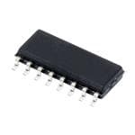
| 供应商器件封装 | 16-SOIC |
| 其它名称 | 296-26653-2 |
| 功率-最大值 | - |
| 包装 | 带卷 (TR) |
| 单位重量 | 141.700 mg |
| 商标 | Texas Instruments |
| 安装类型 | 表面贴装 |
| 安装风格 | SMD/SMT |
| 封装 | Reel |
| 封装/外壳 | 16-SOIC(0.154",3.90mm 宽) |
| 封装/箱体 | SOIC-16 |
| 工厂包装数量 | 2500 |
| 晶体管极性 | NPN |
| 晶体管类型 | 7 NPN 达林顿 |
| 最大工作温度 | + 70 C |
| 最大直流电集电极电流 | 0.5 A |
| 最大集电极截止电流 | 500 uA |
| 最小工作温度 | - 65 C |
| 标准包装 | 2,500 |
| 电压-集射极击穿(最大值) | 100V |
| 电流-集电极(Ic)(最大值) | 500mA |
| 电流-集电极截止(最大值) | - |
| 系列 | SN75468 |
| 配置 | Array 7 |
| 集电极—发射极最大电压VCEO | 100 V |
| 频率-跃迁 | - |


- 商务部:美国ITC正式对集成电路等产品启动337调查
- 曝三星4nm工艺存在良率问题 高通将骁龙8 Gen1或转产台积电
- 太阳诱电将投资9.5亿元在常州建新厂生产MLCC 预计2023年完工
- 英特尔发布欧洲新工厂建设计划 深化IDM 2.0 战略
- 台积电先进制程称霸业界 有大客户加持明年业绩稳了
- 达到5530亿美元!SIA预计今年全球半导体销售额将创下新高
- 英特尔拟将自动驾驶子公司Mobileye上市 估值或超500亿美元
- 三星加码芯片和SET,合并消费电子和移动部门,撤换高东真等 CEO
- 三星电子宣布重大人事变动 还合并消费电子和移动部门
- 海关总署:前11个月进口集成电路产品价值2.52万亿元 增长14.8%


PDF Datasheet 数据手册内容提取
Product Sample & Technical Tools & Support & Folder Buy Documents Software Community SN75468,SN75469 SLRS023E–DECEMBER1976–REVISEDJANUARY2015 SN7546x Darlington Transistor Arrays 1 Features 3 Description • 500-mARatedCollectorCurrent(SingleOutput) The SN75468 and SN75469 are high-voltage, high- 1 current Darlington transistor arrays. Each consists of • High-VoltageOutput100V seven NPN Darlington pairs that feature high-voltage • OutputClampDiodes outputs with common-cathode clamp diodes for • InputsCompatibleWithVariousTypesofLogic switching inductive loads. The collector-current rating of each Darlington pair is 500 mA. The Darlington • RelayDriverApplications pairs may be paralleled for higher current capability. • Higher-VoltageVersionsofULN2003Aand Applications include relay drivers, hammer drivers, ULN2004A,forCommercialTemperaturerange lamp drivers, display drivers (LED and gas discharge),linedrivers,andlogicbuffers. 2 Applications The SN75468 has a 2700-Ω series base resistor for • RelayDrivers each Darlington pair for operation directly with TTL or • HammerDrivers 5-V CMOS. The SN75469 has a 10.5-kΩ series base resistor to allow its operation directly with CMOS or • LampDrivers PMOS that use supply voltages of 6 to 15 V. The • DisplayDrivers(LEDandGasDischarge) requiredinputcurrentisbelowthatoftheSN75468. • LineDrivers DeviceInformation(1) • LogicBuffers PARTNUMBER PACKAGE(PIN) BODYSIZE(NOM) D(16) 9.90mm×3.91mm SN7546x N(16) 19.30mm×6.35mm NS(16) 10.30mm×5.30mm (1) For all available packages, see the orderable addendum at theendofthedatasheet. 4 Simplified Schematic 1 An IMPORTANT NOTICE at the end of this data sheet addresses availability, warranty, changes, use in safety-critical applications, intellectualpropertymattersandotherimportantdisclaimers.PRODUCTIONDATA.
SN75468,SN75469 SLRS023E–DECEMBER1976–REVISEDJANUARY2015 www.ti.com Table of Contents 1 Features.................................................................. 1 9.2 FunctionalBlockDiagram.........................................9 2 Applications........................................................... 1 9.3 FeatureDescription...................................................9 3 Description............................................................. 1 9.4 DeviceFunctionalModes..........................................9 4 SimplifiedSchematic............................................. 1 10 ApplicationandImplementation........................ 10 10.1 ApplicationInformation..........................................10 5 RevisionHistory..................................................... 2 10.2 TypicalApplication ...............................................10 6 PinConfigurationandFunctions......................... 3 10.3 SystemExamples.................................................12 7 Specifications......................................................... 4 11 PowerSupplyRecommendations..................... 14 7.1 AbsoluteMaximumRatings......................................4 12 Layout................................................................... 14 7.2 ESDRatings..............................................................4 12.1 LayoutGuidelines.................................................14 7.3 RecommendedOperatingConditions.......................4 12.2 LayoutExample....................................................14 7.4 ThermalInformation..................................................4 13 DeviceandDocumentationSupport................. 15 7.5 ElectricalCharacteristics...........................................5 7.6 SwitchingCharacteristics..........................................5 13.1 RelatedLinks........................................................15 7.7 TypicalCharacteristics..............................................6 13.2 Trademarks...........................................................15 13.3 ElectrostaticDischargeCaution............................15 8 ParameterMeasurementInformation..................7 13.4 Glossary................................................................15 9 DetailedDescription.............................................. 9 14 Mechanical,Packaging,andOrderable 9.1 Overview...................................................................9 Information........................................................... 15 5 Revision History ChangesfromRevisionD(November2004)toRevisionE Page • AddedApplications,DeviceInformationtable,PinFunctionstable,ESDRatingstable,ThermalInformationtable, TypicalCharacteristics,FeatureDescriptionsection,DeviceFunctionalModes,ApplicationandImplementation section,PowerSupplyRecommendationssection,Layoutsection,DeviceandDocumentationSupportsection,and Mechanical,Packaging,andOrderableInformationsection.................................................................................................. 1 • DeletedOrderingInformationtable........................................................................................................................................ 1 2 SubmitDocumentationFeedback Copyright©1976–2015,TexasInstrumentsIncorporated ProductFolderLinks:SN75468 SN75469
SN75468,SN75469 www.ti.com SLRS023E–DECEMBER1976–REVISEDJANUARY2015 6 Pin Configuration and Functions PinFunctions PIN TYPE DESCRIPTION NAME NO. <1:7>B 1-7 I Channel1through7darlingtonbaseinput <1:7>C 16-10 O Channel1through7darlingtoncollectoroutput E 7 — CommonEmmittersharedbyallchannels(typicallytiedtoground) COM 8 I/O Commoncathodenodeforflybackdiodes(requiredforinductiveloads) Copyright©1976–2015,TexasInstrumentsIncorporated SubmitDocumentationFeedback 3 ProductFolderLinks:SN75468 SN75469
SN75468,SN75469 SLRS023E–DECEMBER1976–REVISEDJANUARY2015 www.ti.com 7 Specifications 7.1 Absolute Maximum Ratings overoperatingfree-airtemperaturerange(unlessotherwisenoted)(1) MIN MAX UNIT V Collector-emittervoltage 100 V CE V Inputvoltage(2) 30 V I Peakcollectorcurrent 500 mA I Outputclampcurrent 500 mA OK Totalemitter-terminalcurrent –2.5 A T Operatingvirtualjunctiontemperature 150 °C J T Storagetemperaturerange –65 150 °C stg (1) StressesbeyondthoselistedunderAbsoluteMaximumRatingsmaycausepermanentdamagetothedevice.Thesearestressratings only,whichdonotimplyfunctionaloperationofthedeviceattheseoranyotherconditionsbeyondthoseindicatedunderRecommended OperatingConditions.Exposuretoabsolute-maximum-ratedconditionsforextendedperiodsmayaffectdevicereliability. (2) Allvoltagevaluesarewithrespecttotheemitter/substrateterminalE,unlessotherwisenoted. 7.2 ESD Ratings VALUE UNIT Humanbodymodel(HBM),perANSI/ESDA/JEDECJS-001,allpins(1) ±2000 V(ESD) Electrostaticdischarge Chargeddevicemodel(CDM),perJEDECspecificationJESD22-C101, V allpins(2) ±500 (1) JEDECdocumentJEP155statesthat500-VHBMallowssafemanufacturingwithastandardESDcontrolprocess. (2) JEDECdocumentJEP157statesthat250-VCDMallowssafemanufacturingwithastandardESDcontrolprocess. 7.3 Recommended Operating Conditions overoperatingfree-airtemperaturerange(unlessotherwisenoted) MIN MAX UNIT V 0 5 V I V 0 100 V CC T JunctionTemperature –40 125 °C J 7.4 Thermal Information SN7546x THERMALMETRIC(1) D UNIT 16PINS R Junction-to-ambientthermalresistance 73 θJA R Junction-to-case(top)thermalresistance 40.3 θJC(top) R Junction-to-boardthermalresistance 38.9 θJB °C/W ψ Junction-to-topcharacterizationparameter 10.9 JT ψ Junction-to-boardcharacterizationparameter 38.7 JB R Junction-to-case(bottom)thermalresistance N/A θJC(bot) (1) Formoreinformationabouttraditionalandnewthermalmetrics,seetheICPackageThermalMetricsapplicationreport,SPRA953. 4 SubmitDocumentationFeedback Copyright©1976–2015,TexasInstrumentsIncorporated ProductFolderLinks:SN75468 SN75469
SN75468,SN75469 www.ti.com SLRS023E–DECEMBER1976–REVISEDJANUARY2015 7.5 Electrical Characteristics T =25°C(unlessotherwisenoted) A SN75468 SN75469 PARAMETER TESTCONDITIONS(1) UNIT MIN TYP MAX MIN TYP MAX IC=125mA IC=200mA 2.4 IC=250mA 2.7 VI(on) On-stateinputvoltage VCE=2V V IC=275mA IC=300mA 3 IC=350mA II=250µA,IC=100mA 0.9 1.1 0.9 1.1 VCE(sat) Collector-emittersaturationvoltage II=350µA,IC=100mA 1 1.3 1 1.3 V II=500µA,IC=100mA 1.2 1.6 1.2 1.6 VF Clamp-diodeforwardvoltage IF=350mA 1.7 2 1.7 2 V VCE=100V,II=0 50 50 ICEX collectorcutoffcurrent VCE=100V, II=0 100 100 µA TA=70°C VI=1V 500 II(off) Off-stateinputcurrent VCE=50V,IC=500µA,TA=70°C 50 65 50 65 µA VI=3.85V 0.93 1.35 II Inputcurrent VI=5V 0.35 0.5 mA VI=12V 1 1.45 VR=100V 50 50 IR Clamp-diodereversecurrent µA VR=100V,TA=70°C 100 10 Ci InputCapacitance VI=0,f=1MHz 15 25 15 25 pF (1) Allelectricalcharacteristicsaremeasuredwith0.1-µFcapacitorsconnectedatREF,CT,andV toGND. CC 7.6 Switching Characteristics T =25°Cfree-airtemperature A PARAMETER TESTCONDITIONS(1) MIN TYP MAX UNIT Propagationdelaytime,low-to-high-level tPLH output VS=20V,RL=163Ω,CL=15pF, 0.25 1 µs Propagationdelaytime,high-to-low-level SeeFigure14 tPHL output 0.25 1 µs VOH High-leveloutputvoltageafterswitching VFiSgu=re5014V,IO=300mA,See VS–20 mV (1) Allswitchingcharacteristicsaremeasuredwith0.1-µFcapacitorsconnectedatREFandV toGND. CC Copyright©1976–2015,TexasInstrumentsIncorporated SubmitDocumentationFeedback 5 ProductFolderLinks:SN75468 SN75469
SN75468,SN75469 SLRS023E–DECEMBER1976–REVISEDJANUARY2015 www.ti.com 7.7 Typical Characteristics Figure1.Collector-EmitterSaturationVoltage Figure2.Collector-EmitterSaturationVoltage vs vs CollectorCurrent(OneDarlington) TotalCollectorCurrent(TwoDarlingtonsinParallel) Figure3.OutputCurrentvsInputCurrent Figure4.DPackageMaximumCollectorCurrent vs DutyCycle Figure5.NPackageMaximumCollectorCurrent vs DutyCycle 6 SubmitDocumentationFeedback Copyright©1976–2015,TexasInstrumentsIncorporated ProductFolderLinks:SN75468 SN75469
SN75468,SN75469 www.ti.com SLRS023E–DECEMBER1976–REVISEDJANUARY2015 8 Parameter Measurement Information Figure6.I Figure7.I CEX CES Figure8.I Figure9.I I(off) I Figure10.V Figure11.h ,V I(on) FE CE(sat) Figure12.I Figure13.V R F Copyright©1976–2015,TexasInstrumentsIncorporated SubmitDocumentationFeedback 7 ProductFolderLinks:SN75468 SN75469
SN75468,SN75469 SLRS023E–DECEMBER1976–REVISEDJANUARY2015 www.ti.com Parameter Measurement Information (continued) A. Thepulsegeneratorhasthefollowingcharacteristics:PRR=12.5kHz,Z =50Ω. O B. CLincludesprobeandjigcapacitance. C. Fortestingthe’468,V =3V;forthe’469,V =8V. IH IH Figure14. TestCircuitandVoltageWaveforms A. Thepulsegeneratorhasthefollowingcharacteristics:PRR=12.5kHz,Z =50Ω. O B. CLincludesprobeandjigcapacitance. C. Fortestingthe’468,V =3V;forthe’469,V =8V. IH IH Figure15. Latch-UpTestCircuitandVoltageWaveforms 8 SubmitDocumentationFeedback Copyright©1976–2015,TexasInstrumentsIncorporated ProductFolderLinks:SN75468 SN75469
SN75468,SN75469 www.ti.com SLRS023E–DECEMBER1976–REVISEDJANUARY2015 9 Detailed Description 9.1 Overview This standard device has proven ubiquity and versatility across a wide range of applications. This is due to its integrationof7Darlingtontransistorsthatarecapableofsinkingupto500mAandwideGPIOrangecapability. The SN75468 comprises seven high voltage, high current NPN Darlington transistor pairs. All units feature a common emitter and open collector outputs. To maximize their effectiveness, these units contain suppression diodes for inductive loads. The SN75468 has a series base resistor to each Darlington pair, thus allowing operation directly with TTL or CMOS operating at supply voltages of 5.0 V or 3.3 V. The SN75468 offers solutions to a great many interface needs, including solenoids, relays, lamps, small motors, and LEDs. Applications requiring sink currents beyond the capability of a single output may be accommodated by paralleling theoutputs. Thisdevicecanoperateoverawidetemperaturerange(–40°Cto105°C). 9.2 Functional Block Diagram 9.3 Feature Description Each channel of SN75468 consists of Darlington connected NPN transistors. This connection creates the effect of a single transistor with a very high current gain (β2). This can be as high as 10,000 A/A at certain currents. The very high β allows for high output current drive with a very low input current, essentially equating to operationwithlowGPIOvoltages. The GPIO voltage is converted to base current via the 2.7 kΩ resistor connected between the input and base of the pre-driver Darlington NPN. The 7.2 kΩ & 3.0 kΩ resistors connected between the base and emitter of each respectiveNPNactaspull-downsandsuppresstheamountofleakagethatmayoccurfromtheinput. The diodes connected between the output and COM pin is used to suppress the kick-back voltage from an inductive load that is excited when the NPN drivers are turned off (stop sinking) and the stored energy in the coilscausesareversecurrenttoflowintothecoilsupplyviathekick-backdiode. In normal operation the diodes on base and collector pins to emitter will be reversed biased. If these diode are forward biased, internal parasitic NPN transistors will draw (a nearly equal) current from other (nearby) device pins. 9.4 Device Functional Modes 9.4.1 InductiveLoadDrive When the COM pin is tied to the coil supply voltage, SN75468 is able to drive inductive loads and supress the kick-backvoltageviatheinternalfreewheelingdiodes. 9.4.2 ResistiveLoadDrive Whendrivingaresistiveload,apull-upresistorisneededinorderforSN75468tosinkcurrentandfortheretobe alogichighlevel.TheCOMpincanbeleftfloatingfortheseapplications. Copyright©1976–2015,TexasInstrumentsIncorporated SubmitDocumentationFeedback 9 ProductFolderLinks:SN75468 SN75469
SN75468,SN75469 SLRS023E–DECEMBER1976–REVISEDJANUARY2015 www.ti.com 10 Application and Implementation NOTE Information in the following applications sections is not part of the TI component specification, and TI does not warrant its accuracy or completeness. TI’s customers are responsible for determining suitability of components for their purposes. Customers should validateandtesttheirdesignimplementationtoconfirmsystemfunctionality. 10.1 Application Information SN75468 will typically be used to drive a high voltage and/or current peripheral from an MCU or logic device that cannot tolerate these conditions. The following design is a common application of SN75468, driving inductive loads.Thisincludesmotors,solenoids & relays.Eachloadtypecanbemodeledbywhat'sseeninFigure16. 10.2 Typical Application VSUP SN75468 IN1 OUT1 IN2 OUT2 3.3 V Logic IN3 OUT3 IN4 OUT4 3.3 V Logic IN5 OUT5 IN6 OUT6 3.3 V Logic IN7 OUT7 VSUP GND COM Figure16. SN75468asInductiveLoadDriver 10.2.1 DesignRequirements Forthisdesignexample,usetheparameterslistedinTable1astheinputparameters. Table1.DesignParameters DESIGNPARAMETER EXAMPLEVALUE GPIOVoltage 3.3Vor5.0V CoilSupplyVoltage 12Vto100V NumberofChannels 7 OutputCurrent(R ) 20mAto300mAperchannel COIL DutyCycle 100% 10 SubmitDocumentationFeedback Copyright©1976–2015,TexasInstrumentsIncorporated ProductFolderLinks:SN75468 SN75469
SN75468,SN75469 www.ti.com SLRS023E–DECEMBER1976–REVISEDJANUARY2015 10.2.2 DetailedDesignProcedure WhenusingSN75468inacoildrivingapplication,determinethefollowing: • Inputvoltagerange • Temperaturerange • Outputanddrivecurrent • Powerdissipation 10.2.2.1 DriveCurrent Thecoilcurrentisdeterminedbythecoilvoltage(VSUP),coilresistance & outputlowvoltage(V orV ). OL CE(SAT) I =(V –V )/R (1) COIL SUP CE(SAT) COIL 10.2.2.2 OutputLowVoltage The output low voltage (V ) is the same thing as V and can be determined by the Electrical OL CE(SAT) Characteristicstable,Figure1,orFigure2. 10.2.2.3 PowerDissipation &Temperature The number of coils driven is dependent on the coil current and on-chip power dissipation. The number of coils drivencanbedeterminedbyFigure4orFigure5. For a more accurate determination of number of coils possible, use the below equation to calculate SN75468 on- chippowerdissipationP : D N P = åV ´I D OLi Li i=1 Where: Nisthenumberofchannelsactivetogether. V istheOUT pinvoltagefortheloadcurrentI .ThisisthesameasV (2) OLi i Li CE(SAT) In order to guarantee reliability of SN75468 and the system the on-chip power dissipation must be lower that or equaltothemaximumallowablepowerdissipation(PD )dictatedbybelowequationEquation3. (MAX) ( ) T -T PD = J(MAX) A (MAX) q JA Where: T isthetargetmaximumjunctiontemperature. J(MAX) T istheoperatingambienttemperature. A θ isthepackagejunctiontoambientthermalresistance. (3) JA It is recommended to limit SN75468 IC’s die junction temperature to less than 125°C. The IC junction temperatureisdirectlyproportionaltotheon-chippowerdissipation. Copyright©1976–2015,TexasInstrumentsIncorporated SubmitDocumentationFeedback 11 ProductFolderLinks:SN75468 SN75469
SN75468,SN75469 SLRS023E–DECEMBER1976–REVISEDJANUARY2015 www.ti.com 10.2.3 ApplicationCurves The following curves were generated with SN75468 driving an OMRON G5NB relay – V = 5.0V; V = 12 V & in sup R =2.8kΩ COIL 13 14 12 11 12 10 V 9 V 10 e - 8 e - g g 8 olta 7 olta v 6 v ut ut 6 p 5 p ut ut O 4 O 4 3 2 2 1 0 0 -0.004 0 0.004 0.008 0.012 0.016 -0.004 0 0.004 0.008 0.012 0.016 Time (s) Time (s) D001 D001 Figure17.OutputResponseWithActivationofCoil(Turn Figure18.OutputResponseWithDe-activationofCoil On) (TurnOff) 10.3 System Examples Figure19. TTLtoLoadSchematic 12 SubmitDocumentationFeedback Copyright©1976–2015,TexasInstrumentsIncorporated ProductFolderLinks:SN75468 SN75469
SN75468,SN75469 www.ti.com SLRS023E–DECEMBER1976–REVISEDJANUARY2015 System Examples (continued) Figure20. BuffertoHigherCurrentLoadsSchematic Figure21. Pull-upResistorSchematic Copyright©1976–2015,TexasInstrumentsIncorporated SubmitDocumentationFeedback 13 ProductFolderLinks:SN75468 SN75469
SN75468,SN75469 SLRS023E–DECEMBER1976–REVISEDJANUARY2015 www.ti.com 11 Power Supply Recommendations This part does not need a power supply; however, the COM pin is typically tied to the system power supply. When this is the case, it is very important to make sure that the output voltage does not heavily exceed the COM pin voltage. This will heavily forward bias the fly-back diodes and cause a large current to flow into COM, potentiallydamagingtheon-chipmetalorover-heatingthepart. 12 Layout 12.1 Layout Guidelines Thin traces can be used on the input due to the low current logic that is typically used to drive SN75468. Care must be taken to separate the input channels as much as possible, as to eliminate cross-talk. Thick traces are recommendedfortheoutput,inordertodrivewhateverhighcurrentsthatmaybeneeded.Wirethicknesscanbe determinedbythetracematerial'scurrentdensityanddesireddrivecurrent. Since all of the channels currents return to a common emitter, it is best to size that trace width to be very wide. Someapplicationsrequireupto2.5A. 12.2 Layout Example 1B 1 16 1C 2B 2 15 2C 3B 3 14 3C 4B 4 13 4C 5B 5 12 5C 6B 6 11 6C 7B 7 10 7C E 8 9 VCOM GND Figure22. PackageLayout 14 SubmitDocumentationFeedback Copyright©1976–2015,TexasInstrumentsIncorporated ProductFolderLinks:SN75468 SN75469
SN75468,SN75469 www.ti.com SLRS023E–DECEMBER1976–REVISEDJANUARY2015 13 Device and Documentation Support 13.1 Related Links The table below lists quick access links. Categories include technical documents, support and community resources,toolsandsoftware,andquickaccesstosampleorbuy. Table2.RelatedLinks TECHNICAL TOOLS& SUPPORT& PARTS PRODUCTFOLDER SAMPLE&BUY DOCUMENTS SOFTWARE COMMUNITY SN75468 Clickhere Clickhere Clickhere Clickhere Clickhere SN75469 Clickhere Clickhere Clickhere Clickhere Clickhere 13.2 Trademarks Alltrademarksarethepropertyoftheirrespectiveowners. 13.3 Electrostatic Discharge Caution Thesedeviceshavelimitedbuilt-inESDprotection.Theleadsshouldbeshortedtogetherorthedeviceplacedinconductivefoam duringstorageorhandlingtopreventelectrostaticdamagetotheMOSgates. 13.4 Glossary SLYZ022—TIGlossary. Thisglossarylistsandexplainsterms,acronyms,anddefinitions. 14 Mechanical, Packaging, and Orderable Information The following pages include mechanical, packaging, and orderable information. This information is the most current data available for the designated devices. This data is subject to change without notice and revision of thisdocument.Forbrowser-basedversionsofthisdatasheet,refertotheleft-handnavigation. Copyright©1976–2015,TexasInstrumentsIncorporated SubmitDocumentationFeedback 15 ProductFolderLinks:SN75468 SN75469
PACKAGE OPTION ADDENDUM www.ti.com 24-Aug-2018 PACKAGING INFORMATION Orderable Device Status Package Type Package Pins Package Eco Plan Lead/Ball Finish MSL Peak Temp Op Temp (°C) Device Marking Samples (1) Drawing Qty (2) (6) (3) (4/5) SN75468D ACTIVE SOIC D 16 40 Green (RoHS CU NIPDAU Level-1-260C-UNLIM 0 to 70 SN75468 & no Sb/Br) SN75468DE4 ACTIVE SOIC D 16 40 Green (RoHS CU NIPDAU Level-1-260C-UNLIM 0 to 70 SN75468 & no Sb/Br) SN75468DR ACTIVE SOIC D 16 2500 Green (RoHS CU NIPDAU Level-1-260C-UNLIM 0 to 70 SN75468 & no Sb/Br) SN75468N ACTIVE PDIP N 16 25 Green (RoHS CU NIPDAU N / A for Pkg Type 0 to 70 SN75468N & no Sb/Br) SN75468NE4 ACTIVE PDIP N 16 25 Green (RoHS CU NIPDAU N / A for Pkg Type 0 to 70 SN75468N & no Sb/Br) SN75468NSR ACTIVE SO NS 16 2000 Green (RoHS CU NIPDAU Level-1-260C-UNLIM 0 to 70 SN75468 & no Sb/Br) SN75468NSRG4 ACTIVE SO NS 16 2000 Green (RoHS CU NIPDAU Level-1-260C-UNLIM 0 to 70 SN75468 & no Sb/Br) SN75469D ACTIVE SOIC D 16 40 Green (RoHS CU NIPDAU Level-1-260C-UNLIM 0 to 70 SN75469 & no Sb/Br) SN75469DE4 ACTIVE SOIC D 16 40 Green (RoHS CU NIPDAU Level-1-260C-UNLIM 0 to 70 SN75469 & no Sb/Br) SN75469DR ACTIVE SOIC D 16 2500 Green (RoHS CU NIPDAU Level-1-260C-UNLIM 0 to 70 SN75469 & no Sb/Br) SN75469N ACTIVE PDIP N 16 25 Green (RoHS CU NIPDAU N / A for Pkg Type 0 to 70 SN75469N & no Sb/Br) (1) The marketing status values are defined as follows: ACTIVE: Product device recommended for new designs. LIFEBUY: TI has announced that the device will be discontinued, and a lifetime-buy period is in effect. NRND: Not recommended for new designs. Device is in production to support existing customers, but TI does not recommend using this part in a new design. PREVIEW: Device has been announced but is not in production. Samples may or may not be available. OBSOLETE: TI has discontinued the production of the device. (2) RoHS: TI defines "RoHS" to mean semiconductor products that are compliant with the current EU RoHS requirements for all 10 RoHS substances, including the requirement that RoHS substance do not exceed 0.1% by weight in homogeneous materials. Where designed to be soldered at high temperatures, "RoHS" products are suitable for use in specified lead-free processes. TI may reference these types of products as "Pb-Free". RoHS Exempt: TI defines "RoHS Exempt" to mean products that contain lead but are compliant with EU RoHS pursuant to a specific EU RoHS exemption. Green: TI defines "Green" to mean the content of Chlorine (Cl) and Bromine (Br) based flame retardants meet JS709B low halogen requirements of <=1000ppm threshold. Antimony trioxide based flame retardants must also meet the <=1000ppm threshold requirement. Addendum-Page 1
PACKAGE OPTION ADDENDUM www.ti.com 24-Aug-2018 (3) MSL, Peak Temp. - The Moisture Sensitivity Level rating according to the JEDEC industry standard classifications, and peak solder temperature. (4) There may be additional marking, which relates to the logo, the lot trace code information, or the environmental category on the device. (5) Multiple Device Markings will be inside parentheses. Only one Device Marking contained in parentheses and separated by a "~" will appear on a device. If a line is indented then it is a continuation of the previous line and the two combined represent the entire Device Marking for that device. (6) Lead/Ball Finish - Orderable Devices may have multiple material finish options. Finish options are separated by a vertical ruled line. Lead/Ball Finish values may wrap to two lines if the finish value exceeds the maximum column width. Important Information and Disclaimer:The information provided on this page represents TI's knowledge and belief as of the date that it is provided. TI bases its knowledge and belief on information provided by third parties, and makes no representation or warranty as to the accuracy of such information. Efforts are underway to better integrate information from third parties. TI has taken and continues to take reasonable steps to provide representative and accurate information but may not have conducted destructive testing or chemical analysis on incoming materials and chemicals. TI and TI suppliers consider certain information to be proprietary, and thus CAS numbers and other limited information may not be available for release. In no event shall TI's liability arising out of such information exceed the total purchase price of the TI part(s) at issue in this document sold by TI to Customer on an annual basis. Addendum-Page 2
PACKAGE MATERIALS INFORMATION www.ti.com 6-Sep-2018 TAPE AND REEL INFORMATION *Alldimensionsarenominal Device Package Package Pins SPQ Reel Reel A0 B0 K0 P1 W Pin1 Type Drawing Diameter Width (mm) (mm) (mm) (mm) (mm) Quadrant (mm) W1(mm) SN75469DR SOIC D 16 2500 330.0 16.4 6.5 10.3 2.1 8.0 16.0 Q1 PackMaterials-Page1
PACKAGE MATERIALS INFORMATION www.ti.com 6-Sep-2018 *Alldimensionsarenominal Device PackageType PackageDrawing Pins SPQ Length(mm) Width(mm) Height(mm) SN75469DR SOIC D 16 2500 333.2 345.9 28.6 PackMaterials-Page2
None
None
None
None
IMPORTANTNOTICEANDDISCLAIMER TIPROVIDESTECHNICALANDRELIABILITYDATA(INCLUDINGDATASHEETS),DESIGNRESOURCES(INCLUDINGREFERENCE DESIGNS),APPLICATIONOROTHERDESIGNADVICE,WEBTOOLS,SAFETYINFORMATION,ANDOTHERRESOURCES“ASIS” ANDWITHALLFAULTS,ANDDISCLAIMSALLWARRANTIES,EXPRESSANDIMPLIED,INCLUDINGWITHOUTLIMITATIONANY IMPLIEDWARRANTIESOFMERCHANTABILITY,FITNESSFORAPARTICULARPURPOSEORNON-INFRINGEMENTOFTHIRD PARTYINTELLECTUALPROPERTYRIGHTS. TheseresourcesareintendedforskilleddevelopersdesigningwithTIproducts.Youaresolelyresponsiblefor(1)selectingtheappropriate TIproductsforyourapplication,(2)designing,validatingandtestingyourapplication,and(3)ensuringyourapplicationmeetsapplicable standards,andanyothersafety,security,orotherrequirements.Theseresourcesaresubjecttochangewithoutnotice.TIgrantsyou permissiontousetheseresourcesonlyfordevelopmentofanapplicationthatusestheTIproductsdescribedintheresource.Other reproductionanddisplayoftheseresourcesisprohibited.NolicenseisgrantedtoanyotherTIintellectualpropertyrightortoanythird partyintellectualpropertyright.TIdisclaimsresponsibilityfor,andyouwillfullyindemnifyTIanditsrepresentativesagainst,anyclaims, damages,costs,losses,andliabilitiesarisingoutofyouruseoftheseresources. TI’sproductsareprovidedsubjecttoTI’sTermsofSale(www.ti.com/legal/termsofsale.html)orotherapplicabletermsavailableeitheron ti.comorprovidedinconjunctionwithsuchTIproducts.TI’sprovisionoftheseresourcesdoesnotexpandorotherwisealterTI’sapplicable warrantiesorwarrantydisclaimersforTIproducts. MailingAddress:TexasInstruments,PostOfficeBox655303,Dallas,Texas75265 Copyright©2019,TexasInstrumentsIncorporated