ICGOO在线商城 > 分立半导体产品 > 晶体管 - 双极 (BJT) - 阵列 > ZXTDBM832TA
 Datasheet下载
- 型号: ZXTDBM832TA
- 制造商: Diodes Inc.
- 库位|库存: xxxx|xxxx
- 要求:
| 数量阶梯 | 香港交货 | 国内含税 |
| +xxxx | $xxxx | ¥xxxx |
查看当月历史价格
查看今年历史价格
ZXTDBM832TA产品简介:
ICGOO电子元器件商城为您提供ZXTDBM832TA由Diodes Inc.设计生产,在icgoo商城现货销售,并且可以通过原厂、代理商等渠道进行代购。 ZXTDBM832TA价格参考。Diodes Inc.ZXTDBM832TA封装/规格:晶体管 - 双极 (BJT) - 阵列, Bipolar (BJT) Transistor Array 2 NPN (Dual) 20V 4.5A 140MHz 1.7W Surface Mount 8-MLP (3x2)。您可以下载ZXTDBM832TA参考资料、Datasheet数据手册功能说明书,资料中有ZXTDBM832TA 详细功能的应用电路图电压和使用方法及教程。
ZXTDBM832TA是Diodes Incorporated推出的一款双极结型晶体管(BJT)阵列,内部集成了两个匹配的NPN晶体管,采用SOT-363小型封装,适用于空间受限的高密度电路设计。该器件具有良好的热稳定性和电气匹配性,常用于需要精确信号处理和高可靠性的场景。

典型应用场景包括:
1. 模拟信号处理电路:如差分放大器、电流镜电路,利用其匹配特性提升电路精度与温度稳定性;
2. 逻辑电平转换与驱动:在数字系统中实现不同电压域之间的信号转换,广泛应用于微控制器接口电路;
3. 电源管理与负载开关:作为小功率开关控制LED、传感器或其他外围设备的通断;
4. 便携式电子设备:因其小尺寸和低功耗特性,适合智能手机、可穿戴设备等对空间和功耗敏感的产品;
5. 工业控制与通信模块:用于信号调理、隔离驱动等场合,提升系统集成度与可靠性。

ZXTDBM832TA凭借其紧凑封装、良好匹配性和稳定性能,在消费电子、工业控制及通信领域具有广泛应用价值。
| 参数 | 数值 |
| 产品目录 | |
| 描述 | TRANS DUAL NPN 20V 4.5A 8MLP |
| 产品分类 | 晶体管(BJT) - 阵列 |
| 品牌 | Diodes/Zetex |
| 数据手册 | |
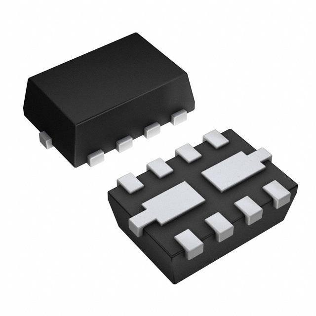
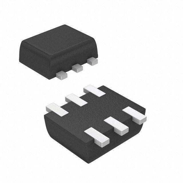
| 产品图片 |
|
| 产品型号 | ZXTDBM832TA |
| PCN过时产品 | |
| rohs | 无铅 / 符合限制有害物质指令(RoHS)规范要求 |
| 产品系列 | - |
| 不同 Ib、Ic时的 Vce饱和值(最大值) | 270mV @ 125mA,4.5A |
| 不同 Ic、Vce 时的DC电流增益(hFE)(最小值) | 200 @ 2A,2V |
| 供应商器件封装 | 8-MLP(3x2) |
| 其它图纸 |
|
| 功率-最大值 | 1.7W |
| 包装 | 带卷 (TR) |
| 安装类型 | 表面贴装 |
| 封装/外壳 | 8-MLP |
| 晶体管类型 | 2 NPN(双) |
| 标准包装 | 3,000 |
| 电压-集射极击穿(最大值) | 20V |
| 电流-集电极(Ic)(最大值) | 4.5A |
| 电流-集电极截止(最大值) | 25nA |
| 频率-跃迁 | 140MHz |


- 商务部:美国ITC正式对集成电路等产品启动337调查
- 曝三星4nm工艺存在良率问题 高通将骁龙8 Gen1或转产台积电
- 太阳诱电将投资9.5亿元在常州建新厂生产MLCC 预计2023年完工
- 英特尔发布欧洲新工厂建设计划 深化IDM 2.0 战略
- 台积电先进制程称霸业界 有大客户加持明年业绩稳了
- 达到5530亿美元!SIA预计今年全球半导体销售额将创下新高
- 英特尔拟将自动驾驶子公司Mobileye上市 估值或超500亿美元
- 三星加码芯片和SET,合并消费电子和移动部门,撤换高东真等 CEO
- 三星电子宣布重大人事变动 还合并消费电子和移动部门
- 海关总署:前11个月进口集成电路产品价值2.52万亿元 增长14.8%


PDF Datasheet 数据手册内容提取
ZXTDBM832 MPPS™ Miniature Package Power Solutions DUAL 20V NPN SILICON LOW SATURATION SWITCHING TRANSISTOR SUMMARY V =20V;R = 47m ;I = 4.5A CEO SAT C DESCRIPTION Packagedintheinnovative3mmx2mmMLP(MicroLeadedPackage)outline, thesenew4thgenerationlowsaturationdualtransistorsofferextremelylowon statelossesmakingthemidealforuseinDC-DCcircuitsandvariousdriving and power management functions. Additionally users gain several otherkey benefits: Performance capability equivalent to much largerpackges Improved circuit efficiency & power levels 3mm x 2mm (Dual die)MLP PCB area and device placement savings Lower package height (nom 0.9mm) C2 C1 Reduced component count FEATURES • Low Equivalent On Resistance B2 B1 • Extremely Low Saturation Voltage(150mV @1A) • h characterised up to 6A FE • I =4.5A Continuous Collector Current C E2 E1 • 3mm x 2mmMLP APPLICATIONS • DC - DC Converters • Charging circuits • Power switches PINOUT • Motor control ORDERING INFORMATION DEVICE REEL TAPE QUANTITY WIDTH PERREEL ZXTDCM832TA 7(cid:1)(cid:1) 8mm 3000 ZXTDCM832TC 13(cid:1)(cid:1) 8mm 10000 DEVICE MARKING 3mm x 2mmMLP DBB underside view ISSUE 1 - JUNE 2002 1
ZXTDBM832 ABSOLUTE MAXIMUM RATINGS. PARAMETER SYMBOL LIMIT UNIT Collector-BaseVoltage VCBO 40 V Collector-EmitterVoltage VCEO 20 V Emitter-BaseVoltage VEBO 7.5 V PeakPulseCurrent ICM 12 A ContinuousCollectorCurrent(a)(f) IC 4.5 A ContinuousCollectorCurrent(b)(f) IC 5 A BaseCurrent IB 1000 mA PowerDissipationatTA=25°C(a)(f) PD 1.5 W LinearDeratingFactor 12 mW/°C PowerDissipationatTA=25°C(b)(f) PD 2.45 W LinearDeratingFactor 19.6 mW/°C PowerDissipationatTA=25°C(c)(f) PD 1 W LinearDeratingFactor 8 mW/°C PowerDissipationatTA=25°C(d)(f) PD 1.13 W LinearDeratingFactor 9 mW/°C PowerDissipationatTA=25°C(d)(g) PD 1.7 W LinearDeratingFactor 13.6 mW/°C PowerDissipationatTA=25°C(e)(g) PD 3 W LinearDeratingFactor 24 mW/°C OperatingandStorageTemperatureRange Tj:Tstg -55 to +150 °C THERMAL RESISTANCE PARAMETER SYMBOL VALUE UNIT JunctiontoAmbient(a)(f) RθJA 83.3 °C/W JunctiontoAmbient(b)(f) RθJA 51 °C/W JunctiontoAmbient(c)(f) RθJA 125 °C/W JunctiontoAmbient(d)(f) RθJA 111 °C/W JunctiontoAmbient(d)(g) RθJA 73.5 °C/W JunctiontoAmbient(e)(g) RθJA 41.7 °C/W Notes (a) For a dual device surface mounted on 8 sq cm single sided 2oz copper on FR4 PCB, in still air conditionswith all exposed pads attached. The copper area is split down the centre line into two separate areas with one half connected to each half of the dual device. (b) Measured at t<5 secs for a dual device surface mounted on 8 sq cm single sided 2oz copper on FR4 PCB, in still air conditionswith all exposed pads attached.The copper area is split down the centre line into two separate areas with one half connected to each half of the dual device. (c) For a dual device surface mounted on 8 sq cm single sided 2oz copper on FR4 PCB, in still air conditionswith minimal lead connections only. (d) For a dual device surface mounted on 10 sq cm single sided 1oz copper on FR4 PCB, in still air conditionswith all exposed pads attached attached. The copper area is split down the centre line into two separate areas with one half connected to each half of the dual device. (e) For a dual device surface mounted on 85 sq cm single sided 2oz copper on FR4 PCB, in still air conditionswith all exposed pads attached attached. The copper area is split down the centre line into two separate areas with one half connected to each half of the dual device. (f) For a dual device with one active die. (g) For dual device with 2 active die running at equal power. (h) Repetitive rating - pulse width limited by max junction temperature. Refer to Transient Thermal Impedance graph. (i) The minimum copper dimensions required for mounting are no smaller than the exposed metal pads on the base of the device as shown in the package dimensions data. The thermal resistance for a dual device mounted on 1.5mm thick FR4 board using minimum copper 1 oz weight, 1mm wide tracks and one half of the device active isRth= 250°C/W giving a power rating ofPtot= 500mW. ISSUE 1 - JUNE 2002 2
ZXTDBM832 TYPICAL CHARACTERISTICS 3.5 nt(A) 10 VLiCmE(SiAtTe)d on(W) 23..50 2NoozteCu(e2)(ogz)Cu Tamb=25°C urre 1 DC pati 2.0 Note(a)(f) C 1s si 1ozCu or 100ms Dis 1.5 Note(d)(g) ect 0.1 10ms er 1.0 Coll0.01 NSoitneg(lae)(Pfu)lse,T =25°C 1ms100us Pow 0.5 1NoozteCu(d)(f) IC amb ax 0.0 0.1 1 10 M 0 25 50 75 100 125 150 V Collector-EmitterVoltage(V) Temperature(°C) CE SafeOperatingArea DeratingCurve 225 W) 80 Note(a)(f) W) 200 1ozcopper C/ C/ 175 Note(f) ° ° 1ozcopper ( 60 ( 150 e e Note(g) c c an D=0.5 an 125 st 40 st 100 si si e e R R 75 mal 20 D=0.2 SinglePulse mal 50 2Noozteco(fp)per er D=0.05 er 25 2ozcopper h D=0.1 h Note(g) T 0 T 0 100µ 1m 10m 100m 1 10 100 1k 0.1 1 10 100 PulseWidth(s) BoardCuArea(sqcm) TransientThermalImpedance ThermalResistancevBoardArea 3.5 T =25°C 2ozcopper 3.0 Tamb=150°C Note(g) W) Cjomnaxtinuous 2.5 ( n o 2.0 2ozcopper ati Note(f) p 1.5 si s Di 1.0 1ozcopper PD 0.5 1ozcopper Note(g) Note(f) 0.0 0.1 1 10 100 BoardCuArea(sqcm) PowerDissipationvBoardArea ISSUE 1 - JUNE 2002 3
ZXTDBM832 ELECTRICAL CHARACTERISTICS (atT = 25°C unless otherwise stated). amb PARAMETER SYMBOL MIN. TYP. MAX. UNIT CONDITIONS. Collector-Base Breakdown V(BR)CBO 40 100 V IC=100(cid:1)A Voltage Collector-EmitterBreakdown V(BR)CEO 20 27 V IC=10mA* Voltage Emitter-Base BreakdownVoltage V(BR)EBO 7.5 8.2 V IE=100(cid:1)A CollectorCut-OffCurrent ICBO 25 nA VCB=32V EmitterCut-OffCurrent IEBO 25 nA VEB=6V CollectorEmitterCut-OffCurrent ICES 25 nA VCES=16V Collector-EmitterSaturation VCE(sat) 8 15 mV IC=0.1A,IB=10mA* Voltage 90 150 mV IC=1A,IB=10mA* 115 135 mV IC=2A,IB=50mA* 190 250 mV IC=3A,IB=100mA* 210 270 mV IC=4.5A,IB=125mA* Base-EmitterSaturationVoltage VBE(sat) 0.98 1.05 V IC=4.5A,IB=125mA* Base-EmitterTurn-OnVoltage VBE(on) 0.88 0.95 V IC=4.5A,VCE=2V* StaticForwardCurrentTransfer hFE 200 400 IC=10mA,VCE=2V* Ratio 300 450 IC=0.2A,VCE=2V* 200 360 IC=2A,VCE=2V* 100 180 IC=6A,VCE=2V* TransitionFrequency fT 100 140 MHz IC=50mA,VCE=10V f=100MHz OutputCapacitance Cobo 23 30 pF VCB=10V,f=1MHz Turn-OnTime t(on) 170 ns VCC=10V,IC=3A Turn-OffTime t(off) 400 ns IB1=IB2=10mA *Measured under pulsed conditions. Pulse width=300µs. Duty cycle≤2% ISSUE 1 - JUNE 2002 4
ZXTDBM832 TYPICAL CHARACTERISTICS 0.25 Tamb=25°C I/I=50 C B 0.20 100m 100°C V) I/I=100 V) 0.15 ( C B ( 25°C SAT)10m SAT)0.10 E( I/I=50 E( VC C B VC -55°C I/I=10 0.05 C B 1m 0.00 1m 10m 100m 1 10 1m 10m 100m 1 10 I CollectorCurrent(A) I CollectorCurrent(A) C C V vI V vI CE(SAT) C CE(SAT) C 630 1.2 VCE=2V 540 1.0 IC/IB=50 edGain 01..80 100°2C5°C 346500ain(h)FE (V) 0.8 -55°C ormalis 00..46 -55°C 128700ypicalG VBE(SAT) 0.6 25°C 100°C N 0.2 90T 0.4 0.0 0 1m 10m 100m 1 10 1m 10m 100m 1 10 I CollectorCurrent(A) I CollectorCurrent(A) C C h vI V vI FE C BE(SAT) C 1.0 V =2V CE 0.8 V) ( -55°C N) E(O 0.6 VB 25°C 0.4 100°C 1m 10m 100m 1 10 I CollectorCurrent(A) C V vI BE(ON) C ISSUE 1 - JUNE 2002 5
ZXTDBM832 MLP832 PACKAGE OUTLINE(3mm x 2mm Micro Leaded Package) CONTROLLING DIMENSIONS IN MILLIMETRES APPROX. CONVERTED DIMENSIONS IN INCHES MLP832 PACKAGE DIMENSIONS MILLIMETRES INCHES MILLIMETRES INCHES DIM DIM MIN. MAX. MIN. MAX. MIN. MAX. MIN. MAX. A 0.80 1.00 0.031 0.039 e 0.65REF 0.0256BSC A1 0.00 0.05 0.00 0.002 E 2.00BSC 0.0787 BSC A2 0.65 0.75 0.0255 0.0295 E2 0.43 0.63 0.017 0.0249 A3 0.15 0.25 0.006 0.0098 E4 0.16 0.36 0.006 0.014 b 0.24 0.34 0.009 0.013 L 0.20 0.45 0.0078 0.0157 b1 0.17 0.30 0.0066 0.0118 L2 0.125 0.00 0.005 D 3.00BSC 0.118BSC r 0.075BSC 0.0029BSC D2 0.82 1.02 0.032 0.040 (cid:2) 0(cid:3) 12(cid:3) 0(cid:3) 12(cid:3) D3 1.01 1.21 0.0397 0.0476 ©Zetexplc 2002 Europe Americas Asia Pacific Zetexplc ZetexGmbH ZetexInc Zetex(Asia) Ltd Fields New Road Streitfeldstraße19 700 Veterans Memorial Hwy 3701-04Metroplaza, Tower 1 Chadderton D-81673 München Hauppauge, NY11788 HingFongRoad Oldham, OL9 8NP KwaiFong United Kingdom Germany USA Hong Kong Telephone (44) 161 622 4422 Telefon: (49) 89 45 49 49 0 Telephone: (631) 360 2222 Telephone: (852) 26100 611 Fax: (44) 161 622 4420 Fax: (49) 89 45 49 49 49 Fax: (631) 360 8222 Fax: (852) 24250 494 uksales@zetex.com europe.sales@zetex.com usa.sales@zetex.com asia.sales@zetex.com These offices are supported by agents and distributors in major countries world-wide. Thispublicationisissuedtoprovideoutlineinformationonlywhich(unlessagreedbytheCompanyinwriting)maynotbeused,appliedorreproduced foranypurposeorformpartofanyorderorcontractorberegardedasarepresentationrelatingtotheproductsorservicesconcerned.TheCompany reserves the right to alter without notice the specification, design, price or conditions of supply of any product or service. Forthelatestproductinformation,logontowww.zetex.com ISSUE 1 - JUNE 2002 6