ICGOO在线商城 > 分立半导体产品 > 晶体管 - 双极 (BJT) - 阵列 > ZXTD617MCTA
 Datasheet下载
- 型号: ZXTD617MCTA
- 制造商: Diodes Inc.
- 库位|库存: xxxx|xxxx
- 要求:
| 数量阶梯 | 香港交货 | 国内含税 |
| +xxxx | $xxxx | ¥xxxx |
查看当月历史价格
查看今年历史价格
ZXTD617MCTA产品简介:
ICGOO电子元器件商城为您提供ZXTD617MCTA由Diodes Inc.设计生产,在icgoo商城现货销售,并且可以通过原厂、代理商等渠道进行代购。 ZXTD617MCTA价格参考。Diodes Inc.ZXTD617MCTA封装/规格:晶体管 - 双极 (BJT) - 阵列, Bipolar (BJT) Transistor Array 2 NPN (Dual) 15V 4.5A 120MHz 1.7W Surface Mount 8-DFN (3x2)。您可以下载ZXTD617MCTA参考资料、Datasheet数据手册功能说明书,资料中有ZXTD617MCTA 详细功能的应用电路图电压和使用方法及教程。
Diodes Incorporated的ZXTD617MCTA是一款双极性晶体管(BJT)阵列器件,常用于需要高增益、低噪声和良好高频性能的电子电路中。该器件内部包含多个BJT晶体管,适合需要多管协同工作的应用场景。

ZXTD617MCTA的主要应用场景包括:

1. 射频(RF)放大器:该器件具有良好的高频响应特性,适用于无线通信设备中的射频信号放大,如Wi-Fi模块、蓝牙模块和蜂窝通信系统。

2. 音频放大电路:由于其低噪声和高增益特性,ZXTD617MCTA也适用于音频前置放大器和低功率音频放大器设计。

3. 开关电路:在需要多个晶体管协同工作的多路开关或逻辑控制电路中,该器件可简化设计并节省PCB空间。

4. 传感器接口电路:用于传感器信号的放大与处理,尤其是在需要高精度和稳定性的工业控制和测量设备中。

5. 电源管理电路:在某些DC-DC转换器或负载开关中,可用于实现高效的电流控制和功率调节。

综上,ZXTD617MCTA适用于通信、音频处理、工业控制等多个领域,具备高性能与集成化优势,适合对空间和性能有要求的电子设计。
| 参数 | 数值 |
| 产品目录 | |
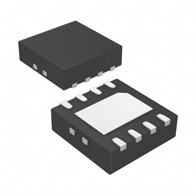
| 描述 | TRANS DUAL NPN 15V 4.5A 8DFN |
| 产品分类 | 晶体管(BJT) - 阵列 |
| 品牌 | Diodes Incorporated |
| 数据手册 | |
| 产品图片 |
|
| 产品型号 | ZXTD617MCTA |
| rohs | 无铅 / 符合限制有害物质指令(RoHS)规范要求 |
| RoHS指令信息 | http://diodes.com/download/4349 |
| 产品系列 | - |
| 不同 Ib、Ic时的 Vce饱和值(最大值) | 310mV @ 50mA,4.5A |
| 不同 Ic、Vce 时的DC电流增益(hFE)(最小值) | 200 @ 3A,2V |
| 供应商器件封装 | 8-DFN(3x2) |
| 其它名称 | ZXTD617MCTADKR |
| 功率-最大值 | 1.7W |
| 包装 | Digi-Reel® |
| 安装类型 | 表面贴装 |
| 封装/外壳 | 8-WDFN 裸露焊盘 |
| 晶体管类型 | 2 NPN(双) |
| 标准包装 | 1 |
| 电压-集射极击穿(最大值) | 15V |
| 电流-集电极(Ic)(最大值) | 4.5A |
| 电流-集电极截止(最大值) | 100nA |
| 频率-跃迁 | 120MHz |


- 商务部:美国ITC正式对集成电路等产品启动337调查
- 曝三星4nm工艺存在良率问题 高通将骁龙8 Gen1或转产台积电
- 太阳诱电将投资9.5亿元在常州建新厂生产MLCC 预计2023年完工
- 英特尔发布欧洲新工厂建设计划 深化IDM 2.0 战略
- 台积电先进制程称霸业界 有大客户加持明年业绩稳了
- 达到5530亿美元!SIA预计今年全球半导体销售额将创下新高
- 英特尔拟将自动驾驶子公司Mobileye上市 估值或超500亿美元
- 三星加码芯片和SET,合并消费电子和移动部门,撤换高东真等 CEO
- 三星电子宣布重大人事变动 还合并消费电子和移动部门
- 海关总署:前11个月进口集成电路产品价值2.52万亿元 增长14.8%


PDF Datasheet 数据手册内容提取
A Product Line of Diodes Incorporated ZXTD 617MC DUAL 15V NPN LOW SATURATION TRANSISTORS Features and Benefits Mechanical Data • BVCEO > 15V • Case: DFN3020B-8 • IC = 4.5A Continuous Collector Current • Case Material: Molded Plastic. “Green” Molding Compound. • Low Saturation Voltage (100mV max @ 1A) • Terminals: Pre-Plated NiPdAu leadframe • RSAT = 45 mΩ for a Low Equivalent On-Resistance • UL Flammability Rating 94V-0 • hFE specified up to 12A for high current gain hold up • Nominal Package Height: 0.8mm • Dual NPN saving footprint and component count • Moisture Sensitivity: Level 1 per J-STD-020 • Low profile 0.8mm high package for thin applications • Weight: 0.013 grams (approximate) • RθJA efficient, 40% lower than SOT26 • 6mm2 footprint, 50% smaller than TSOP6 and SOT26 • Lead-Free, RoHS Compliant (Note 1) Applications • Halogen and Antimony Free. “Green” Device (Note 2) • Qualified to AEC-Q101 Standards for High Reliability • DC-DC Converters • Charging circuits • Motor control • Power switches • Portable applications C2 C1 DFN3020B-8 C2 C2 C1 C1 B2 B1 C2 C1 E2 B2 E1 B1 E2 E1 Pin 1 Top View Bottom View NPN Transistor NPN Transistor Bottom View Pin-Out Equivalent Circuit Ordering Information Product Marking Reel size (inches) Tape width (mm) Quantity per reel ZXTD617MCTA DAA 7 8 3000 Notes: 1. No purposefully added lead. 2. Diodes Inc’s “Green” Policy can be found on our website at http://www.diodes.com Marking Information DAA = Product type marking code DAA Top view, dot denotes pin 1 ZXTD617MC 1 of 7 December 2010 Document Number DS31930 Rev. 3 - 2 www.diodes.com © Diodes Incorporated
A Product Line of Diodes Incorporated ZXTD617MC Maximum Ratings @TA = 25°C unless otherwise specified Characteristic Symbol Value Unit Collector-Base Voltage VCBO 40 Collector-Emitter Voltage VCEO 15 V Emitter-Base Voltage VEBO 7 Peak Pulse Current ICM 15 (Notes 3 & 6) 4.5 Continuous Collector Current (Notes 4 & 6) IC 5 A Base Current IB 1 Thermal Characteristics @ TA = 25°C unless otherwise specified Characteristic Symbol Value Unit 1.5 (Notes 3 & 6) 12 2.45 (Notes 4 & 6) Power Dissipation 19.6 W Linear Derating Factor PD 1.13 mW/°C (Notes 5 & 6) 8 1.7 (Notes 5 & 7) 13.6 (Notes 3 & 6) 83.3 (Notes 4 & 6) 51.0 Thermal Resistance, Junction to Ambient (Notes 5 & 6) RθJA 111 °C/W (Notes 5 & 7) 73.5 Thermal Resistance, Junction to Lead (Notes 6 & 8) RθJL 17.1 Operating and Storage Temperature Range TJ, TSTG -55 to +150 °C Notes: 3. For a dual device surface mounted on 28mm x 28mm (8cm2) FR4 PCB with high coverage of single sided 2 oz copper, in still air conditions; the device is measured when operating in a steady-state condition. The heatsink is split in half with the exposed collector pads connected to each half. 4. Same as note (3), except the device is measured at t <5 sec. 5. Same as note (3), except the device is surface mounted on 31mm x 31mm (10cm2) FR4 PCB with high coverage of single sided 1oz copper. 6. For a dual device with one active die. 7. For dual device with 2 active die running at equal power. 8. Thermal resistance from junction to solder-point (at the end of the collector lead). ZXTD617MC 2 of 7 December 2010 Document Number DS31930 Rev. 3 - 2 www.diodes.com © Diodes Incorporated
A Product Line of Diodes Incorporated ZXTD617MC Thermal Characteristics 2.0 10sqcm 1oz Cu ) 10 VCE(SAT) W) Two active die A Limited nt ( on ( 1.5 8sqcm 2oz Cu rre 1 DC ati One active die u p C 1s si 1.0 10sqcm 1oz Cu ctor 0.1 100ms 10ms Dis One active die Colle 8Osnqec mac t2ivoez dCieu 1ms 100us ower 0.5 I C0.01 Single Pulse, Tamb=25°C ax P 0.0 0.1 1 10 M 0 25 50 75 100 125 150 V Collector-Emitter Voltage (V) Temperature (°C) CE Safe Operating Area Derating Curve 225 ) 80 8sqcm 2oz Cu ) 200 W W 1oz Cu One active die C/ C/ 175 One active die ° ° 1oz Cu e ( 60 e ( 150 Two active die c c n D=0.5 n 125 a a st 40 st 100 si si e e 75 R D=0.2 Single Pulse R 2oz Cu al 20 al 50 One active die m D=0.05 m 2oz Cu r r 25 he D=0.1 he Two active die T 0 T 0 100µ 1m 10m 100m 1 10 100 1k 0.1 1 10 100 Pulse Width (s) Board Cu Area (sqcm) Transient Thermal Impedance Thermal Resistance v Board Area 3.5 T =25°C 2oz Cu amb 3.0 T =150°C Two active die ) j max W Continuous 2.5 ( n o 2.0 2oz Cu ati One active die p 1.5 si s Di 1.0 D 1oz Cu P 0.5 1oz Cu Two active die One active die 0.0 0.1 1 10 100 Board Cu Area (sqcm) Power Dissipation v Board Area ZXTD617MC 3 of 7 December 2010 Document Number DS31930 Rev. 3 - 2 www.diodes.com © Diodes Incorporated
A Product Line of Diodes Incorporated ZXTD617MC Electrical Characteristics @TA = 25°C unless otherwise specified Characteristic Symbol Min Typ Max Unit Test Condition Collector-Base Breakdown Voltage BVCBO 40 70 - V IC = 100µA Collector-Emitter Breakdown Voltage (Note 9) BVCEO 15 18 - V IC = 10mA Emitter-Base Breakdown Voltage BVEBO 7 8.2 - V IE = 100µA Collector Cutoff Current ICBO - - 100 nA VCB = 30V Emitter Cutoff Current IEBO - - 100 nA VEB = 6V Collector Emitter Cutoff Current ICES - - 100 nA VCES = 12V 200 415 - - IC = 10mA, VCE = 2V 300 450 - - IC = 200mA, VCE = 2V Static Forward Current Transfer Ratio (Note 9) hFE 200 320 - - IC = 3A, VCE = 2V 150 240 - - IC = 5A, VCE = 2V - 80 - - IC = 12A, VCE= 2V - 8 14 mV IC =0.1A, IB = 10mA - 70 100 mV IC = 1A, IB = 10mA Collector-Emitter Saturation Voltage (Note 9) VCE(sat) - 165 200 mV IC = 3A, IB = 50mA - 240 310 mV IC =4.5A, IB = 50mA - 200 - mV IC =4.5A, IB= 100mA Base-Emitter Turn-On Voltage (Note 9) VBE(on) - 0.88 0.96 V IC = 4.5A, VCE= 2V Base-Emitter Saturation Voltage (Note 9) VBE(sat) - 0.94 1.05 V IC = 4.5A, IB= 50mA Output Capacitance Cobo - 30 40 pF VCB = 10V. f = 1MHz Transition Frequency fT 80 120 - MHz Vf =C E1 =0 01M0VH,z I C = 50mA, Turn-on Time ton - 120 - ns VCC = 10V, IC = 1A Turn-off Time toff - 160 - ns IB1 = IB2 = 10mA Notes: 9. Measured under pulsed conditions. Pulse width ≤ 300 µs. Duty cycle ≤ 2% ZXTD617MC 4 of 7 December 2010 Document Number DS31930 Rev. 3 - 2 www.diodes.com © Diodes Incorporated
A Product Line of Diodes Incorporated ZXTD617MC Typical Electrical Characteristics 1 0.25 Tamb=25°C I/I=50 C B 0.20 100m V) V) 0.15 100°C ( ( AT) IC/IB=100 AT)0.10 25°C S S E(10m E( C C V I/I=50 V -55°C C B 0.05 I/I=10 C B 1m 0.00 1m 10m 100m 1 10 1m 10m 100m 1 10 I Collector Current (A) I Collector Current (A) C C V v I V v I CE(SAT) C CE(SAT) C 630 1.2 VCE=2V 540 1.0 IC/IB=50 100°C n 1.0 450)E ai hF malised G 000...468 25°-C55°C 123876000cal Gain ( (V)BE(SAT) 00..68 -55°C25°C or pi V 100°C N 0.2 90 Ty 0.4 0.0 0 1m 10m 100m 1 10 1m 10m 100m 1 10 I Collector Current (A) I Collector Current (A) C C h v I V v I FE C BE(SAT) C 1.0 V =2V CE 0.8 ) V -55°C ( N) 0.6 O E( 25°C B V 0.4 100°C 0.2 1m 10m 100m 1 10 I Collector Current (A) C V v I BE(ON) C ZXTD617MC 5 of 7 December 2010 Document Number DS31930 Rev. 3 - 2 www.diodes.com © Diodes Incorporated
A Product Line of Diodes Incorporated ZXTD617MC Package Outline Dimensions DFN3020B-8 A A3 Dim Min Max Typ A 0.77 0.83 0.80 A1 A1 0 0.05 0.02 A3 - - 0.15 D b 0.25 0.35 0.30 D 2.95 3.075 3.00 D2 0.82 1.02 0.92 D4 1.01 1.21 1.11 D4 D4 e - - 0.65 D2 E 1.95 2.075 2.00 E E2 E2 0.43 0.63 0.53 L 0.25 0.35 0.30 Z b e Z - - 0.375 L All Dimensions in mm Suggested Pad Layout C X Dimensions Value (in mm) Y1 C 0.650 G G1 G 0.285 G1 0.090 Y2 X 0.400 Y X1 1.120 Y 0.730 X1 Y1 0.500 Y2 0.365 ZXTD617MC 6 of 7 December 2010 Document Number DS31930 Rev. 3 - 2 www.diodes.com © Diodes Incorporated
A Product Line of Diodes Incorporated ZXTD617MC IMPORTANT NOTICE DIODES INCORPORATED MAKES NO WARRANTY OF ANY KIND, EXPRESS OR IMPLIED, WITH REGARDS TO THIS DOCUMENT, INCLUDING, BUT NOT LIMITED TO, THE IMPLIED WARRANTIES OF MERCHANTABILITY AND FITNESS FOR A PARTICULAR PURPOSE (AND THEIR EQUIVALENTS UNDER THE LAWS OF ANY JURISDICTION). Diodes Incorporated and its subsidiaries reserve the right to make modifications, enhancements, improvements, corrections or other changes without further notice to this document and any product described herein. Diodes Incorporated does not assume any liability arising out of the application or use of this document or any product described herein; neither does Diodes Incorporated convey any license under its patent or trademark rights, nor the rights of others. Any Customer or user of this document or products described herein in such applications shall assume all risks of such use and will agree to hold Diodes Incorporated and all the companies whose products are represented on Diodes Incorporated website, harmless against all damages. Diodes Incorporated does not warrant or accept any liability whatsoever in respect of any products purchased through unauthorized sales channel. Should Customers purchase or use Diodes Incorporated products for any unintended or unauthorized application, Customers shall indemnify and hold Diodes Incorporated and its representatives harmless against all claims, damages, expenses, and attorney fees arising out of, directly or indirectly, any claim of personal injury or death associated with such unintended or unauthorized application. Products described herein may be covered by one or more United States, international or foreign patents pending. Product names and markings noted herein may also be covered by one or more United States, international or foreign trademarks. LIFE SUPPORT Diodes Incorporated products are specifically not authorized for use as critical components in life support devices or systems without the express written approval of the Chief Executive Officer of Diodes Incorporated. As used herein: A. Life support devices or systems are devices or systems which: 1. are intended to implant into the body, or 2. support or sustain life and whose failure to perform when properly used in accordance with instructions for use provided in the labeling can be reasonably expected to result in significant injury to the user. B. A critical component is any component in a life support device or system whose failure to perform can be reasonably expected to cause the failure of the life support device or to affect its safety or effectiveness. Customers represent that they have all necessary expertise in the safety and regulatory ramifications of their life support devices or systems, and acknowledge and agree that they are solely responsible for all legal, regulatory and safety-related requirements concerning their products and any use of Diodes Incorporated products in such safety-critical, life support devices or systems, notwithstanding any devices- or systems-related information or support that may be provided by Diodes Incorporated. Further, Customers must fully indemnify Diodes Incorporated and its representatives against any damages arising out of the use of Diodes Incorporated products in such safety-critical, life support devices or systems. Copyright © 2010, Diodes Incorporated www.diodes.com ZXTD617MC 7 of 7 December 2010 Document Number DS31930 Rev. 3 - 2 www.diodes.com © Diodes Incorporated
Mouser Electronics Authorized Distributor Click to View Pricing, Inventory, Delivery & Lifecycle Information: D iodes Incorporated: ZXTD617MCTA