ICGOO在线商城 > 分立半导体产品 > 晶体管 - 双极 (BJT) - 阵列 > BC858CDXV6T1G
 Datasheet下载
- 型号: BC858CDXV6T1G
- 制造商: ON Semiconductor
- 库位|库存: xxxx|xxxx
- 要求:
| 数量阶梯 | 香港交货 | 国内含税 |
| +xxxx | $xxxx | ¥xxxx |
查看当月历史价格
查看今年历史价格
BC858CDXV6T1G产品简介:
ICGOO电子元器件商城为您提供BC858CDXV6T1G由ON Semiconductor设计生产,在icgoo商城现货销售,并且可以通过原厂、代理商等渠道进行代购。 BC858CDXV6T1G价格参考。ON SemiconductorBC858CDXV6T1G封装/规格:晶体管 - 双极 (BJT) - 阵列, Bipolar (BJT) Transistor Array 2 PNP (Dual) 30V 100mA 100MHz 500mW Surface Mount SOT-563。您可以下载BC858CDXV6T1G参考资料、Datasheet数据手册功能说明书,资料中有BC858CDXV6T1G 详细功能的应用电路图电压和使用方法及教程。
型号为 BC858CDXV6T1G 的晶体管属于 ON Semiconductor 生产的 双极型晶体管(BJT)阵列,常用于需要多个晶体管集成封装的电路设计中。该器件内部通常包含两个或多个独立的 NPN 或 PNP 晶体管,具有小型化、一致性好和布线简洁的优点。

 主要应用场景包括:

1. 信号放大电路:适用于音频、射频等小信号放大器的设计,尤其在便携式电子设备中节省空间。
2. 开关电路:用于数字电路中的逻辑控制、继电器驱动、LED 显示驱动等场合。
3. 接口电路:在微控制器与外围设备之间实现电平转换或电流增强功能。
4. 传感器电路:作为传感器信号处理中的增益调节或缓冲元件。
5. 消费类电子产品:如手机、平板电脑、智能穿戴设备等对体积敏感的产品中。
6. 工业自动化:用于 PLC 控制模块、继电器板卡等工业控制系统中。

该器件采用 SOT-26 或类似小型表面贴装封装,适合高密度 PCB 设计,并具备良好的热稳定性和可靠性。
| 参数 | 数值 |
| 产品目录 | |
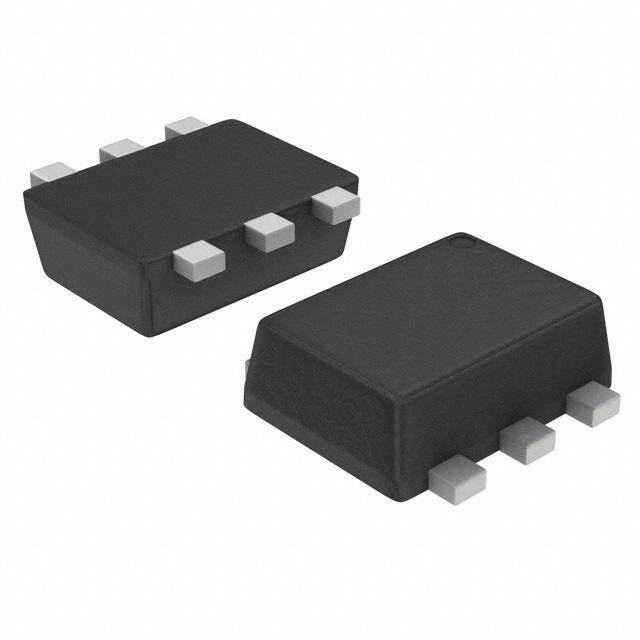
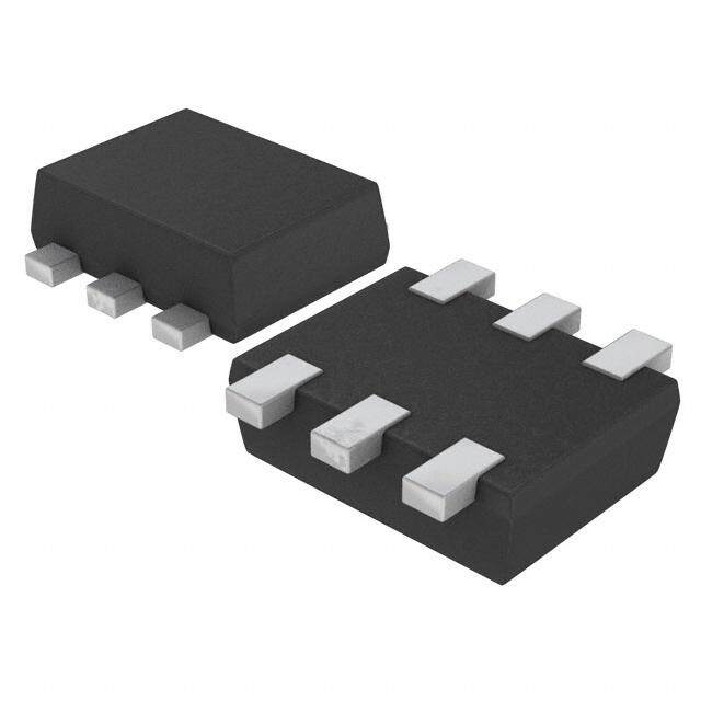
| 描述 | TRANS PNP DUAL 30V 100MA SOT-563两极晶体管 - BJT 100mA 30V Dual PNP |
| 产品分类 | 晶体管(BJT) - 阵列分离式半导体 |
| 品牌 | ON Semiconductor |
| 产品手册 | |
| 产品图片 |
|
| rohs | 符合RoHS无铅 / 符合限制有害物质指令(RoHS)规范要求 |
| 产品系列 | 晶体管,两极晶体管 - BJT,ON Semiconductor BC858CDXV6T1G- |
| 数据手册 | |
| 产品型号 | BC858CDXV6T1G |
| PCN组件/产地 | |
| PCN设计/规格 | |
| 不同 Ib、Ic时的 Vce饱和值(最大值) | 650mV @ 5mA,100mA |
| 不同 Ic、Vce 时的DC电流增益(hFE)(最小值) | 420 @ 2mA,5V |
| 产品种类 | 两极晶体管 - BJT |
| 供应商器件封装 | SOT-563 |
| 其它名称 | BC858CDXV6T1GOSDKR |
| 功率-最大值 | 500mW |
| 包装 | Digi-Reel® |
| 发射极-基极电压VEBO | 5 V |
| 商标 | ON Semiconductor |
| 增益带宽产品fT | 100 MHz |
| 安装类型 | 表面贴装 |
| 安装风格 | SMD/SMT |
| 封装 | Reel |
| 封装/外壳 | SOT-563,SOT-666 |
| 封装/箱体 | SOT-563-6 |
| 工厂包装数量 | 4000 |
| 晶体管极性 | PNP |
| 晶体管类型 | 2 PNP(双) |
| 最大功率耗散 | 357 mW |
| 最大工作温度 | + 150 C |
| 最大直流电集电极电流 | 0.1 A |
| 最小工作温度 | - 55 C |
| 标准包装 | 1 |
| 电压-集射极击穿(最大值) | 30V |
| 电流-集电极(Ic)(最大值) | 100mA |
| 电流-集电极截止(最大值) | 15nA (ICBO) |
| 直流集电极/BaseGainhfeMin | 420 |
| 系列 | BC858CDXV6 |
| 配置 | Dual |
| 集电极—发射极最大电压VCEO | - 30 V |
| 集电极—基极电压VCBO | - 30 V |
| 集电极—射极饱和电压 | - 0.65 V |
| 集电极连续电流 | - 0.1 A |
| 频率-跃迁 | 100MHz |


- 商务部:美国ITC正式对集成电路等产品启动337调查
- 曝三星4nm工艺存在良率问题 高通将骁龙8 Gen1或转产台积电
- 太阳诱电将投资9.5亿元在常州建新厂生产MLCC 预计2023年完工
- 英特尔发布欧洲新工厂建设计划 深化IDM 2.0 战略
- 台积电先进制程称霸业界 有大客户加持明年业绩稳了
- 达到5530亿美元!SIA预计今年全球半导体销售额将创下新高
- 英特尔拟将自动驾驶子公司Mobileye上市 估值或超500亿美元
- 三星加码芯片和SET,合并消费电子和移动部门,撤换高东真等 CEO
- 三星电子宣布重大人事变动 还合并消费电子和移动部门
- 海关总署:前11个月进口集成电路产品价值2.52万亿元 增长14.8%


PDF Datasheet 数据手册内容提取
BC858CDXV6T1, BC858CDXV6T5 Dual General Purpose Transistor PNP Dual http://onsemi.com This transistor is designed for general purpose amplifier applications. It is housed in the SOT−563 which is designed for low power surface mount applications. (3) (2) (1) Features • These are Pb−Free Devices Q1 Q2 MAXIMUM RATINGS (4) (5) (6) Rating Symbol Value Unit Collector−Emitter Voltage VCEO −30 V Collector−Base Voltage VCBO −30 V 6 Emitter−Base Voltage VEBO −5.0 V 1 Collector Current − Continuous IC −100 mAdc Maximum ratings are those values beyond which device damage can occur. Maximum ratings applied to the device are individual stress limit values (not SOT−563 normal operating conditions) and are not valid simultaneously. If these limits are CASE 463A exceeded, device functional operation is not implied, damage may occur and PLASTIC reliability may be affected. THERMAL CHARACTERISTICS MARKING DIAGRAMS Characteristic (One Junction Heated) Symbol Max Unit Total Device Dissipation, (Note 1) PD TA = 25°C 357 mW 3L M(cid:2) Derate above 25°C 2.9 mW/°C (cid:2) Thermal Resistance R(cid:2)JA 350 °C/W 1 Junction-to-Ambient (Note 1) Characteristic (Both Junctions Heated) Symbol Max Unit 3L =Device Code M =Date Code Total Device Dissipation, (Note 1) PD (cid:2) =Pb−Free Package TA = 25°C 500 mW Derate above 25°C 4.0 mW/°C (Note: Microdot may be in either location) Thermal Resistance R(cid:2)JA 250 °C/W ORDERING INFORMATION Junction-to-Ambient (Note 1) Device Package Shipping† Junction and Storage TJ, Tstg −55 to +150 °C Temperature Range BC858CDXV6T1 SOT−563 4000/Tape & Reel 1. FR−4 @ Minimum Pad BC858CDXV6T1G SOT−563 4000/Tape & Reel (Pb−Free) BC858CDXV6T5 SOT−563 8000/Tape & Reel BC858CDXV6T5G SOT−563 8000/Tape & Reel (Pb−Free) †For information on tape and reel specifications, including part orientation and tape sizes, please refer to our Tape and Reel Packaging Specifications Brochure, BRD8011/D. © Semiconductor Components Industries, LLC, 2005 1 Publication Order Number: October, 2005 − Rev. 3 BC858CDXV6T1/D
BC858CDXV6T1, BC858CDXV6T5 ELECTRICAL CHARACTERISTICS (TA = 25°C unless otherwise noted) Characteristic Symbol Min Typ Max Unit OFF CHARACTERISTICS Collector−Emitter Breakdown Voltage V(BR)CEO V (IC = −10 mA) −30 − − Collector−Emitter Breakdown Voltage V(BR)CES V (IC = −10 (cid:3)A, VEB = 0) −30 − − Collector−Base Breakdown Voltage V(BR)CBO V (IC = −10 (cid:3)A) −30 − − Emitter−Base Breakdown Voltage V(BR)EBO V (IE = −1.0 (cid:3)A) −5.0 − − Collector Cutoff Current (VCB = −30 V) ICBO − − −15 nA Collector Cutoff Current (VCB = −30 V, TA = 150°C) − − −4.0 (cid:3)A ON CHARACTERISTICS DC Current Gain hFE − (IC = −10 (cid:3)A, VCE = −5.0 V) − 270 − (IC = −2.0 mA, VCE = −5.0 V) 420 520 800 Collector−Emitter Saturation Voltage VCE(sat) V (IC = −10 mA, IB = −0.5 mA) − − −0.3 (IC = −100 mA, IB = −5.0 mA) − − −0.65 Base−Emitter Saturation Voltage VBE(sat) V (IC = −10 mA, IB = −0.5 mA) − −0.7 − (IC = −100 mA, IB = −5.0 mA) − −0.9 − Base−Emitter On Voltage VBE(on) V (IC = −2.0 mA, VCE = −5.0 V) −0.6 − −0.75 (IC = −10 mA, VCE = −5.0 V) − − −0.82 SMALL−SIGNAL CHARACTERISTICS Current−Gain − Bandwidth Product fT 100 − − MHz (IC = −10 mA, VCE = −5.0 Vdc, f = 100 MHz) Output Capacitance Cob − − 4.5 pF (VCB = −10 V, f = 1.0 MHz) Noise Figure NF − − 10 dB (IC = −0.2 mA, VCE = −5.0 Vdc, RS = 2.0 k(cid:4), f = 1.0 kHz, BW = 200 Hz) http://onsemi.com 2
BC858CDXV6T1, BC858CDXV6T5 TYPICAL CHARACTERISTICS 2.0 −1.0 AIN 1.5 VCE = −10 V −0.9 TA = 25°C T G TA = 25°C −0.8 VBE(sat) @ IC/IB = 10 N RE 1.0 S) −0.7 R T DC CU 0.7 E (VOL −−00..65 VBE(on) @ VCE = −10 V ZED 0.5 LTAG −0.4 LI O A V RM V, −0.3 O , NFE 0.3 −−00..21 VCE(sat) @ IC/IB = 10 h 0.2 0 −0.2 −0.5 −1.0 −2.0 −5.0 −10 −20 −50 −100 −200 −0.1 −0.2 −0.5 −1.0 −2.0 −5.0 −10 −20 −50 −100 I , COLLECTOR CURRENT (mAdc) I , COLLECTOR CURRENT (mAdc) C C Figure 1. Normalized DC Current Gain Figure 2. “Saturation” and “On” Voltages −2.0 1.0 LTAGE (V) −1.6 TA = 25°C T (mV/C)° 1.2 −55°C to +125°C O N R V CIE 1.6 E −1.2 FI T F T E EMI CO 2.0 CTOR− −0.8 I−C1 0= mA IC = −50 mA IC = −200 mA ATURE 2.4 V, COLLECE −0.4 IC = −20 mA IC = −100 mA , TEMPERVB 2.8 0 θ −0.02 −0.1 −1.0 −10 −20 −0.2 −1.0 −10 −100 I , BASE CURRENT (mA) I , COLLECTOR CURRENT (mA) B C Figure 3. Collector Saturation Region Figure 4. Base−Emitter Temperature Coefficient z) 10 H 400 M Cib CT ( 300 7.0 U D TA = 25°C RO 200 pF) 5.0 H P 150 V = −10 V TANCE ( 3.0 Cob NDWIDT 100 TAC E= 25°C C, CAPACI 2.0 GAIN − BA 8600 − 40 T N E 30 R R U 1.0 C 20 −0.4 −0.6 −1.0 −2.0 −4.0 −6.0 −10 −20 −30 −40 (cid:2), T −0.5 −1.0 −2.0 −3.0 −5.0 −10 −20 −30 −50 f V , REVERSE VOLTAGE (VOLTS) I , COLLECTOR CURRENT (mAdc) R C Figure 5. Capacitances Figure 6. Current−Gain − Bandwidth Product http://onsemi.com 3
BC858CDXV6T1, BC858CDXV6T5 PACKAGE DIMENSIONS SOT−563, 6 LEAD CASE 463A−01 ISSUE F D NOTES: A 1. DIMENSIONING AND TOLERANCING PER ANSI −X− Y14.5M, 1982. L 2. CONTROLLING DIMENSION: MILLIMETERS 3. MAXIMUM LEAD THICKNESS INCLUDES LEAD FINISH THICKNESS. MINIMUM LEAD THICKNESS 6 5 4 IS THE MINIMUM THICKNESS OF BASE MATERIAL. E −Y− HE MILLIMETERS INCHES 1 2 3 DIM MIN NOM MAX MIN NOM MAX A 0.50 0.55 0.60 0.020 0.021 0.023 b 0.17 0.22 0.27 0.007 0.009 0.011 b 65 PL C C 0.08 0.12 0.18 0.003 0.005 0.007 e 0.08 (0.003)M X Y DE 11..5100 11..6200 11..7300 00..005493 00..006427 00..006561 e 0.5 BSC 0.02 BSC L 0.10 0.20 0.30 0.004 0.008 0.012 HE 1.50 1.60 1.70 0.059 0.062 0.066 STYLE 1: PIN 1.EMITTER 1 2.BASE 1 3.COLLECTOR 2 4.EMITTER 2 5.BASE 2 6.COLLECTOR 1 SOLDERING FOOTPRINT* 0.3 0.0118 0.45 0.0177 1.0 1.35 0.0394 0.0531 0.5 0.5 (cid:2) (cid:3) 0.0197 0.0197 SCALE 20:1 mm inches *For additional information on our Pb−Free strategy and soldering details, please download the ON Semiconductor Soldering and Mounting Techniques Reference Manual, SOLDERRM/D. ON Semiconductor and are registered trademarks of Semiconductor Components Industries, LLC (SCILLC). SCILLC reserves the right to make changes without further notice to any products herein. SCILLC makes no warranty, representation or guarantee regarding the suitability of its products for any particular purpose, nor does SCILLC assume any liability arising out of the application or use of any product or circuit, and specifically disclaims any and all liability, including without limitation special, consequential or incidental damages. “Typical” parameters which may be provided in SCILLC data sheets and/or specifications can and do vary in different applications and actual performance may vary over time. All operating parameters, including “Typicals” must be validated for each customer application by customer’s technical experts. SCILLC does not convey any license under its patent rights nor the rights of others. SCILLC products are not designed, intended, or authorized for use as components in systems intended for surgical implant into the body, or other applications intended to support or sustain life, or for any other application in which the failure of the SCILLC product could create a situation where personal injury or death may occur. Should Buyer purchase or use SCILLC products for any such unintended or unauthorized application, Buyer shall indemnify and hold SCILLC and its officers, employees, subsidiaries, affiliates, and distributors harmless against all claims, costs, damages, and expenses, and reasonable attorney fees arising out of, directly or indirectly, any claim of personal injury or death associated with such unintended or unauthorized use, even if such claim alleges that SCILLC was negligent regarding the design or manufacture of the part. SCILLC is an Equal Opportunity/Affirmative Action Employer. This literature is subject to all applicable copyright laws and is not for resale in any manner. PUBLICATION ORDERING INFORMATION LITERATURE FULFILLMENT: N. American Technical Support: 800−282−9855 Toll Free ON Semiconductor Website: http://onsemi.com Literature Distribution Center for ON Semiconductor USA/Canada P.O. Box 61312, Phoenix, Arizona 85082−1312 USA Order Literature: http://www.onsemi.com/litorder Phone: 480−829−7710 or 800−344−3860 Toll Free USA/Canada Japan: ON Semiconductor, Japan Customer Focus Center Fax: 480−829−7709 or 800−344−3867 Toll Free USA/Canada 2−9−1 Kamimeguro, Meguro−ku, Tokyo, Japan 153−0051 For additional information, please contact your Email: orderlit@onsemi.com Phone: 81−3−5773−3850 local Sales Representative. http://onsemi.com BC858CDXV6T1/D 4
Mouser Electronics Authorized Distributor Click to View Pricing, Inventory, Delivery & Lifecycle Information: O N Semiconductor: BC858CDXV6T1G