ICGOO在线商城 > 分立半导体产品 > 晶体管 - FET,MOSFET - 单 > IRFI4227PBF
/IRFI4227PBF.jpg)
 Datasheet下载
- 型号: IRFI4227PBF
- 制造商: International Rectifier
- 库位|库存: xxxx|xxxx
- 要求:
| 数量阶梯 | 香港交货 | 国内含税 |
| +xxxx | $xxxx | ¥xxxx |
查看当月历史价格
查看今年历史价格
IRFI4227PBF产品简介:
ICGOO电子元器件商城为您提供IRFI4227PBF由International Rectifier设计生产,在icgoo商城现货销售,并且可以通过原厂、代理商等渠道进行代购。 IRFI4227PBF价格参考¥15.41-¥15.41。International RectifierIRFI4227PBF封装/规格:晶体管 - FET,MOSFET - 单, 通孔 N 沟道 200V 26A(Tc) 46W(Tc) TO-220AB 整包。您可以下载IRFI4227PBF参考资料、Datasheet数据手册功能说明书,资料中有IRFI4227PBF 详细功能的应用电路图电压和使用方法及教程。
Infineon Technologies的IRFI4227PBF是一款N沟道增强型MOSFET(金属氧化物半导体场效应晶体管),其主要应用场景包括:

1. 开关电源:该器件适用于各种开关电源设计,例如DC-DC转换器、反激式变换器和升压变换器。其低导通电阻(Rds(on))特性有助于提高效率,降低功耗。

2. 电机驱动:IRFI4227PBF可用于小型直流电机或步进电机的驱动电路中,提供高效的开关性能和良好的电流承载能力。

3. 负载切换:在需要频繁开启或关闭负载的应用中,如汽车电子系统中的负载切换,这款MOSFET可以快速响应并保持稳定运行。

4. 电池管理:用于电池保护和管理系统中,控制充电和放电过程,确保电池安全工作在规定范围内。

5. 逆变器:在小型光伏逆变器或其他类型的逆变器中作为功率开关元件使用,帮助实现交流与直流之间的转换。

6. 电信设备:适用于通信基础设施中的信号放大和处理模块,比如基站功率放大器等。

7. 消费类电子产品:如家用电器、笔记本电脑适配器等领域,提供高效能比的同时满足紧凑型设计需求。

总之,凭借其优秀的电气参数(如耐压值、电流容量及低导通电阻等),IRFI4227PBF非常适合应用于需要高性能功率转换和控制的各种场合。
| 参数 | 数值 |
| 产品目录 | |
| ChannelMode | Enhancement |
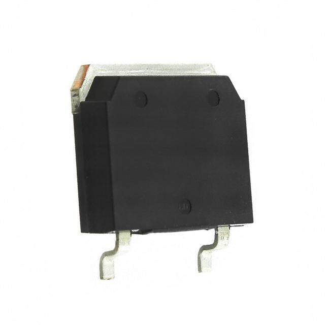
| 描述 | MOSFET N-CH 200V 26A TO-220FPMOSFET MOSFT 200V 26A 22mOhm 73nC |
| 产品分类 | FET - 单分离式半导体 |
| FET功能 | 标准 |
| FET类型 | MOSFET N 通道,金属氧化物 |
| Id-ContinuousDrainCurrent | 26 A |
| Id-连续漏极电流 | 26 A |
| 品牌 | International Rectifier |
| 产品手册 | |
| 产品图片 |
|
| rohs | 符合RoHS无铅 / 符合限制有害物质指令(RoHS)规范要求 |
| 产品系列 | 晶体管,MOSFET,International Rectifier IRFI4227PBFHEXFET® |
| 数据手册 | |
| 产品型号 | IRFI4227PBF |
| PCN组件/产地 | |
| PCN设计/规格 | |
| Pd-PowerDissipation | 46 W |
| Pd-功率耗散 | 46 W |
| Qg-GateCharge | 73 nC |
| Qg-栅极电荷 | 73 nC |
| RdsOn-Drain-SourceResistance | 25 mOhms |
| RdsOn-漏源导通电阻 | 25 mOhms |
| Vds-Drain-SourceBreakdownVoltage | 200 V |
| Vds-漏源极击穿电压 | 200 V |
| Vgs-Gate-SourceBreakdownVoltage | +/- 30 V |
| Vgs-栅源极击穿电压 | 30 V |
| 上升时间 | 19 ns |
| 下降时间 | 29 ns |
| 不同Id时的Vgs(th)(最大值) | 5V @ 250µA |
| 不同Vds时的输入电容(Ciss) | 4600pF @ 25V |
| 不同Vgs时的栅极电荷(Qg) | 110nC @ 10V |
| 不同 Id、Vgs时的 RdsOn(最大值) | 25 毫欧 @ 17A,10V |
| 产品培训模块 | http://www.digikey.cn/PTM/IndividualPTM.page?site=cn&lang=zhs&ptm=26250 |
| 产品种类 | MOSFET |
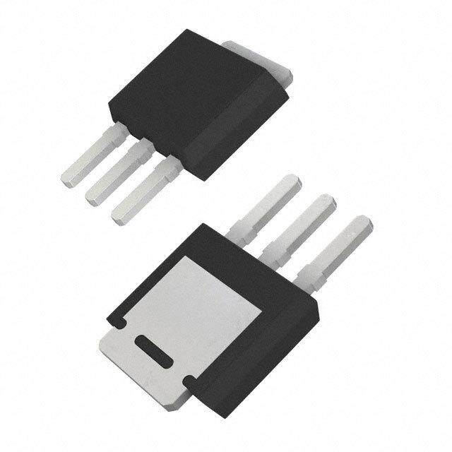
| 供应商器件封装 | TO-220AB 整包 |
| 典型关闭延迟时间 | 11 ns |
| 功率-最大值 | 46W |
| 功率耗散 | 46 W |
| 包装 | 管件 |
| 商标 | International Rectifier |
| 安装类型 | 通孔 |
| 安装风格 | Through Hole |
| 导通电阻 | 25 mOhms |
| 封装 | Tube |
| 封装/外壳 | TO-220-3 整包 |
| 封装/箱体 | TO-220FP-3 |
| 工厂包装数量 | 50 |
| 晶体管极性 | N-Channel |
| 最大工作温度 | + 150 C |
| 最小工作温度 | - 40 C |
| 栅极电荷Qg | 73 nC |
| 标准包装 | 50 |
| 正向跨导-最小值 | 47 S |
| 汲极/源极击穿电压 | 200 V |
| 漏极连续电流 | 26 A |
| 漏源极电压(Vdss) | 200V |
| 电流-连续漏极(Id)(25°C时) | 26A (Tc) |
| 设计资源 | http://www.irf.com/product-info/models/saber/irfi4227pbf.sinhttp://www.irf.com/product-info/models/spice/irfi4227pbf.spi |
| 通道模式 | Enhancement |
| 配置 | Single |
| 闸/源击穿电压 | +/- 30 V |


- 商务部:美国ITC正式对集成电路等产品启动337调查
- 曝三星4nm工艺存在良率问题 高通将骁龙8 Gen1或转产台积电
- 太阳诱电将投资9.5亿元在常州建新厂生产MLCC 预计2023年完工
- 英特尔发布欧洲新工厂建设计划 深化IDM 2.0 战略
- 台积电先进制程称霸业界 有大客户加持明年业绩稳了
- 达到5530亿美元!SIA预计今年全球半导体销售额将创下新高
- 英特尔拟将自动驾驶子公司Mobileye上市 估值或超500亿美元
- 三星加码芯片和SET,合并消费电子和移动部门,撤换高东真等 CEO
- 三星电子宣布重大人事变动 还合并消费电子和移动部门
- 海关总署:前11个月进口集成电路产品价值2.52万亿元 增长14.8%


PDF Datasheet 数据手册内容提取
IRFI4227PbF Features HEXFET® Power MOSFET Advanced Process Technology Key Parameters Key Parameters Optimized for PDP Sustain, Energy Recovery and Pass Switch Applications VDS max 200 V Low E Rating to Reduce Power PULSE V typ. 240 V DS (Avalanche) Dissipation in PDP Sustain, Energy Recovery and Pass Switch Applications RDS(ON) typ. @ 10V 21 m Low Q for Fast Response G I max @ T = 100°C 47 A RP C High Repetitive Peak Current Capability for T max 150 °C Reliable Operation J Short Fall & Rise Times for Fast Switching 150°C Operating Junction Temperature for Improved Ruggedness Repetitive Avalanche Capability for Robustness and Reliability S D G TO-220 Full-Pak G D S Gate Drain Source Description This HEXFET® Power MOSFET is specifically designed for Sustain; Energy Recovery & Pass switch applications in Plasma Display Panels. This MOSFET utilizes the latest processing techniques to achieve low on-resistance per silicon area and low EPULSE rating. Additional features of this MOSFET are 150°C operating junction temperature and high repetitive peak current capability. These features combine to make this MOSFET a highly efficient, robust and reliable device for PDP driving applications Standard Pack Base Part Number Package Type Orderable Part Number Form Quantity IRFI4227PbF TO-220 Full-Pak Tube 50 IRFI4227PbF Absolute Maximum Ratings Symbol Parameter Max. Units VGS Gate-to-Source Voltage ± 30 V I @ T = 25°C Continuous Drain Current, V @ 10V 26 D C GS I @ T = 100°C Continuous Drain Current, V @ 10V 17 D C GS A I Pulsed Drain Current 100 DM I @ T = 100°C Repetitive Peak Current 47 RP C P @T = 25°C Maximum Power Dissipation 46 W D C P @T = 100°C Maximum Power Dissipation 18 D C Linear Derating Factor 0.37 W/°C T Operating Junction and J -40 to + 150 T Storage Temperature Range °C STG Soldering Temperature, for 10 seconds (1.6mm from case) 300 Mounting torque, 6-32 or M3 screw 10 lbf•in (1.1N•m) Thermal Resistance Symbol Parameter Typ. Max. Units R Junction-to-Case ––– 2.73 JC °C/W R Junction-to-Ambient ––– 65 JA 1 2017-04-27
IRFI4227PbF Electrical Characteristics @ T = 25°C (unless otherwise specified) J Parameter Min. Typ. Max. Units Conditions V Drain-to-Source Breakdown Voltage 200 ––– ––– V V = 0V, I = 250µA (BR)DSS GS D V /T Breakdown Voltage Temp. Coefficient ––– 240 ––– mV/°C Reference to 25°C, I = 1mA (BR)DSS J D R Static Drain-to-Source On-Resistance ––– 21 25 m V = 10V, I = 17A DS(on) GS D V Gate Threshold Voltage 3.0 ––– 5.0 V GS(th) V = V , I = 250µA DS GS D V T Gate Threshold Voltage Temp. Coefficient ––– -11 ––– mV/°C GS(th)/ J ––– ––– 20 µA V = 200V, V = 0V I Drain-to-Source Leakage Current DS GS DSS ––– ––– 1.0 mA V = 200V,V = 0V,T =150°C DS GS J Gate-to-Source Forward Leakage ––– ––– 100 V = 20V I nA GS GSS Gate-to-Source Reverse Leakage ––– ––– -100 V = -20V GS gfs Forward Trans conductance 47 ––– ––– S V = 25V, I = 17A DS D Q Total Gate Charge ––– 73 110 I = 17A,V = 100V g nC D DS Q Gate-to-Drain Charge ––– 21 ––– V = 10V gd GS t Turn-On Delay Time ––– 17 ––– V = 100V, V = 10V d(on) DD GS t Rise Time ––– 19 ––– I = 17A r ns D t Turn-Off Delay Time ––– 11 ––– R = 2.5 d(off) G t Fall Time ––– 29 ––– See Fig. 22 f t Shoot Through Blocking Time 100 ––– ––– ns V = 160V,V = 15V,R = 4.7 st DD GS G L = 220nH, C = 0.4µF, V = 15V ––– 570 ––– GS V = 160V, R = 4.7T = 25°C E Energy per Pulse µJ DD G J PULSE L = 220nH, C = 0.4µF, V = 15V ––– 910 ––– GS V = 160V, R = 4.7T = 100°C DD G J C Input Capacitance ––– 4600 ––– V = 0V iss GS C Output Capacitance ––– 460 ––– V = 25V oss DS pF C Reverse Transfer Capacitance ––– 91 ––– ƒ = 1.0MHz rss C eff. Effective Output Capacitance ––– 360 ––– V = 0V, V = 20V to 160V oss GS DS Between lead, L Internal Drain Inductance ––– 4.5 ––– D 6mm (0.25in.) nH from package L Internal Source Inductance ––– 7.5 ––– S and center of die contact Avalanche Characteristics Parameter Typ. Max. Units E Single Pulse Avalanche Energy ––– 54 AS mJ E Repetitive Avalanche Energy ––– 4.6 AR V Repetitive Avalanche Voltage 240 ––– V DS(Avalanche) I Avalanche Current ––– 16 A AS Diode Characteristics Parameter Min. Typ. Max. Units Conditions Continuous Source Current MOSFET symbol I @ T = 25°C ––– ––– 26 S C (Body Diode) showing the A Pulsed Source Current integral reverse I ––– ––– 100 SM (Body Diode) p-n junction diode. V Diode Forward Voltage ––– ––– 1.3 V T = 25°C,I = 17A,V = 0V SD J S GS t Reverse Recovery Time ––– 93 140 ns T = 25°C ,I = 17A, V = 50V rr J F DD Q Reverse Recovery Charge ––– 350 520 nC di/dt = 100A/µs rr Notes: Repetitive rating; pulse width limited by max. junction temperature. starting T = 25°C, L = 0.44mH, R = 25, I = 16A. J G AS Pulse width 400µs; duty cycle 2%. R is measured at T of approximately 90°C. θ J Half sine wave with duty cycle = 0.25, ton=1μsec. 2 2017-04-27
IRFI4227PbF VGS VGS TOP 15V 7.0V TOP 15V )An(t e 100 BOTTOM 1870..00VVV )An(t e 100 BOTTOM 1870..00VVV 7.0V urr urr C C e e c c ru ru o o S S -o -o n-t n-t ia ia Dr Dr , D 10 , D 10 I I 60µs PULSE WIDTH 60µs PULSE WIDTH Tj = 25°C Tj = 150°C 0.1 1 10 100 0.1 1 10 100 V , Drain-to-Source Voltage (V) V , Drain-to-Source Voltage (V) DS DS Fig. 1. Typical Output Characteristics Fig. 2. Typical Output Characteristics 1000.0 3.0 VDS = 25V e c ID = 17A n t )en 100.0 60µs PULSE WIDTH atRessi 2.5 VGS = 10V urr On 2.0 Cce Souron--tDa ri,ID 110..00 TJ = 150°C TJ = 25°C oucerSo--tanriD, Rn) DoS(d)azeliNmor ( 011...505 0.1 0.0 3.0 4.0 5.0 6.0 7.0 8.0 -60 -40 -20 0 20 40 60 80 100 120 140 160 VGS, Gate-to-Source Voltage (V) TJ , Junction Temperature (°C) Fig. 3. Typical Transfer Characteristics Fig. 4. Normalized On-Resistance vs. Temperature 1000 1000 L = 220nH L = 220nH 900 C = 0.4µF C = Variable 100°C 100°C 800 800 25°C 25°C J) µJ) µe( 700 se( 600 slu 600 lpu per er p yp 500 gy 400 gre 400 rne n E E 300 200 200 0 100 130 140 150 160 170 180 190 110 120 130 140 150 160 170 I Peak Drain Current (A) V Drain-to -Source Voltage (V) D, DS, Fig 5. Typical E vs. Drain-to-Source Voltage Fig 6. Typical E vs. Drain Current PULSE PULSE 3 2017-04-27
IRFI4227PbF 1400 1000.0 L = 220nH 1200 J) 1000 CC== 00..43µµFF A()ent 100.0 TJ = 150°C eµ( C= 0.2µF Curr slpu 800 n ia er Dr 10.0 gyp 600 erse TJ = 25°C Ener 400 v,Re D 1.0 S I 200 VGS = 0V 0 0.1 25 50 75 100 125 150 0.2 0.4 0.6 0.8 1.0 1.2 1.4 Temperature (°C) VSD, Source-to-Drain Voltage (V) Fig. 7. Typical E vs. Temperature Fig 8. Typical Source-Drain Diode Forward Voltage PULSE 8000 20 VGS = 0V, f = 1 MHZ ID= 17A Ciss = Cgs + Cgd, Cds SHORTED 6000 CCrossss == CCdgsd + Cgd V)(ge 16 VVDDSS== 116000VV )F aolt VDS= 40V p V e( Ciss e 12 c c anitc 4000 urSo apaC o-te- 8 C, Coss atG 2000 , SG 4 V Crss 0 0 1 10 100 1000 0 20 40 60 80 100 120 VDS, Drain-to-Source Voltage (V) QG Total Gate Charge (nC) Fig 9. Typical Capacitance vs.Drain-to-Source Voltage Fig 10. Typical Gate Charge vs. Gate-to-Source Voltage 30 1000 OPERATION IN THIS AREA LIMITED BY RDS(on) )A )A en(t 100 1µsec n(t 20 Curr eurr ce 10µsec Canri DI , D 10 urSoot-anr-iD 110 100µsec , D Tc = 25°C I Tj = 150°C Single Pulse 0 0.1 25 50 75 100 125 150 1 10 100 1000 TC , CaseTemperature (°C) VDS , Drain-to-Source Voltage (V) Fig 11. Maximum Drain Current vs. Case Temperature Fig 12. Maximum Safe Operating Area 4 2017-04-27
IRFI4227PbF ) 0.16 240 e( c ID = 17A J)m ID an y( 200 TOP 2.5A stResi 0.12 ngerE B O T T O M 31.60AA On che 160 e an ucr 0.08 alv 120 o A Sot- an-i TJ = 125°C e Pus le 80 rD 0.04 ngl ), on iSS, 40 (S TJ = 25°C EA D R 0.00 0 5 6 7 8 9 10 25 50 75 100 125 150 VGS, Gate-to-Source Voltage (V) Starting TJ, Junction Temperature (°C) Fig. 14. Maximum Avalanche Energy Vs. Temperature Fig. 13. On-Resistance Vs. Gate Voltage 5.0 80 ton= 1µs V) Duty cycle = 0.25 ( ageltVod 44..05 ID = 250µA A)(t enurr 60 HSqaulfa Srein Pe uWlsaeve lo C eshhr 3.5 ak Pe 40 e t e tGa) Sh(t 3.0 evtitiRep 20 G 2.5 V 2.0 0 -75 -50 -25 0 25 50 75 100 125 150 25 50 75 100 125 150 TJ , Temperature ( °C ) Case Temperature (°C) Fig. 15. Threshold Voltage vs. Temperature Fig. 16. Typical Repetitive peak Current vs. Case temperature 10 ) D = 0.50 C 1 J h 0.20 Zt ( e sonpseR la 0.1 0000....10000152 JJ1C1i= iRiR1R1 2R22R2 R33R33 CC R00i. .4(9°4C098/7W58 ) 00..10i 00(s50e31c27)97 m Ci= iRi 1.3717 2.0127 reh 0.01 T SINGLE PULSE Notes: ( THERMAL RESPONSE ) 1. Duty Factor D = t1/t2 2. Peak Tj = P dm x Zthjc + Tc 0.001 1E-006 1E-005 0.0001 0.001 0.01 0.1 1 10 t1 , Rectangular Pulse Duration (sec) Fig 17. Maximum Effective Transient Thermal Impedance, Junction-to-Case 5 2017-04-27
IRFI4227PbF Fig 18. Diode Reverse Recovery Test Circuit for N-Channel HEXFET® Power MOSFETs Fig 19a. Unclamped Inductive Test Circuit Fig 19b. Unclamped Inductive Waveforms Fig 20a. Gate Charge Test Circuit Fig 20b. Gate Charge Waveform 6 2017-04-27
IRFI4227PbF Fig 21a. t and E Test Circuit Fig 21b. t Test Waveforms st PULSE st Fig 21c. E Test Waveforms PULSE Fig 22a. Switching Time Test Circuit Fig 22b. Switching Time Waveforms 7 2017-04-27
IRFI4227PbF TO-220 Full-Pak Package Outline (Dimensions are shown in millimeters (inches)) TO-220 Full-Pak Part Marking Information TO-220AB Full-Pak packages are not recommended for Surface Mount Application. Note: For the most current drawing please refer to website at http://www.irf.com/package/ 8 2017-04-27
IRFI4227PbF Qualification Information Industrial Qualification Level (per JEDEC JESD47F) † Moisture Sensitivity Level TO-220 Full-Pak N/A RoHS Compliant Yes † Applicable version of JEDEC standard at the time of product release. Revision History Date Comments Changed datasheet with Infineon logo - all pages. 04/27/2017 Corrected Package Outline on page 8. Added disclaimer on last page. Trademarks of Infineon Technologies AG µHVIC™, µIPM™, µPFC™, AU-ConvertIR™, AURIX™, C166™, CanPAK™, CIPOS™, CIPURSE™, CoolDP™, CoolGaN™, COOLiR™, CoolMOS™, CoolSET™, CoolSiC™, DAVE™, DI-POL™, DirectFET™, DrBlade™, EasyPIM™, EconoBRIDGE™, EconoDUAL™, EconoPACK™, EconoPIM™, EiceDRIVER™, eupec™, FCOS™, GaNpowIR™, HEXFET™, HITFET™, HybridPACK™, iMOTION™, IRAM™, ISOFACE™, IsoPACK™, LEDrivIR™, LITIX™, MIPAQ™, ModSTACK™, my-d™, NovalithIC™, OPTIGA™, OptiMOS™, ORIGA™, PowIRaudio™, PowIRStage™, PrimePACK™, PrimeSTACK™, PROFET™, PRO-SIL™, RASIC™, REAL3™, SmartLEWIS™, SOLID FLASH™, SPOC™, StrongIRFET™, SupIRBuck™, TEMPFET™, TRENCHSTOP™, TriCore™, UHVIC™, XHP™, XMC™ Trademarks updated November 2015 Other Trademarks All referenced product or service names and trademarks are the property of their respective owners. Edition 2016-04-19 IMPORTANT NOTICE For further information on the product, technology, The information given in this document shall in no Published by event be regarded as a guarantee of conditions or delivery terms and conditions and prices please contact your nearest Infineon Technologies office Infineon Technologies AG characteristics (“Beschaffenheitsgarantie”) . (www.infineon.com). 81726 Munich, Germany With respect to any examples, hints or any typical values stated herein and/or any information Please note that this product is not qualified © 2016 Infineon Technologies AG. regarding the application of the product, Infineon according to the AEC Q100 or AEC Q101 documents All Rights Reserved. Technologies hereby disclaims any and all of the Automotive Electronics Council. warranties and liabilities of any kind, including without limitation warranties of non-infringement Do you have a question about this of intellectual property rights of any third party. WARNINGS document? Due to technical requirements products may Email: erratum@infineon.com In addition, any information given in this contain dangerous substances. For information on document is subject to customer’s compliance the types in question please contact your nearest with its obligations stated in this document and Infineon Technologies office. any applicable legal requirements, norms and Document reference standards concerning customer’s products and Except as otherwise explicitly approved by Infineon ifx1 any use of the product of Infineon Technologies in Technologies in a written document signed by customer’s applications. authorized representatives of Infineon Technologies, Infineon Technologies’ products The data contained in this document is exclusively may not be used in any applications where a intended for technically trained staff. It is the failure of the product or any consequences of the responsibility of customer’s technical use thereof can reasonably be expected to result in departments to evaluate the suitability of the personal injury. product for the intended application and the completeness of the product information given in this document with respect to such application. 9 2017-04-27
Mouser Electronics Authorized Distributor Click to View Pricing, Inventory, Delivery & Lifecycle Information: I nfineon: IRFI4227PBF