ICGOO在线商城 > 分立半导体产品 > 晶体管 - FET,MOSFET - 单 > DMN2300UFD-7
 Datasheet下载
- 型号: DMN2300UFD-7
- 制造商: Diodes Inc.
- 库位|库存: xxxx|xxxx
- 要求:
| 数量阶梯 | 香港交货 | 国内含税 |
| +xxxx | $xxxx | ¥xxxx |
查看当月历史价格
查看今年历史价格
DMN2300UFD-7产品简介:
ICGOO电子元器件商城为您提供DMN2300UFD-7由Diodes Inc.设计生产,在icgoo商城现货销售,并且可以通过原厂、代理商等渠道进行代购。 DMN2300UFD-7价格参考。Diodes Inc.DMN2300UFD-7封装/规格:晶体管 - FET,MOSFET - 单, 表面贴装 N 沟道 20V 1.21A(Ta) 470mW(Ta) X1-DFN1212-3。您可以下载DMN2300UFD-7参考资料、Datasheet数据手册功能说明书,资料中有DMN2300UFD-7 详细功能的应用电路图电压和使用方法及教程。
Diodes Incorporated的DMN2300UFD-7是一款N沟道增强型MOSFET(金属氧化物场效应晶体管),其应用场景非常广泛,尤其适用于需要高效、低功耗和小尺寸解决方案的电子设备中。以下是该型号MOSFET的一些典型应用场景:

 1. 电源管理
   DMN2300UFD-7常用于各种电源管理电路中,如DC-DC转换器、线性稳压器等。它能够提供高效的开关性能,降低导通电阻(Rds(on)),从而减少功率损耗,提高整体效率。此外,它的低栅极电荷特性使得它在高频开关应用中表现出色,适合用于笔记本电脑、智能手机和平板电脑等便携式设备的电源管理系统。

 2. 负载开关
   在负载开关应用中,DMN2300UFD-7可以作为开关元件,控制电流的通断。它能够在低电压下快速响应,确保系统的稳定性和可靠性。例如,在USB接口、电池管理系统和其他需要精确控制电流的应用中,该MOSFET可以有效防止过流、短路等问题,保护电路免受损坏。

 3. 电机驱动
   该MOSFET也适用于小型电机驱动应用,如风扇、泵和小型机器人等。它可以提供足够的电流驱动能力,同时保持较低的功耗和发热。通过精确控制电机的启停和转速,DMN2300UFD-7有助于提高系统的响应速度和能效。

 4. 信号切换
   在信号切换电路中,DMN2300UFD-7可以用作高速开关,实现不同信号路径之间的切换。由于其低导通电阻和快速开关特性,它能够确保信号的完整性,减少信号失真和噪声干扰。这种应用场景常见于通信设备、音频处理系统等。

 5. 消费电子
   该MOSFET广泛应用于消费电子产品中,如智能手表、可穿戴设备、智能家居产品等。这些设备通常对体积和功耗有严格要求,而DMN2300UFD-7的小封装(DFN2020-6)和低功耗特性使其成为理想选择。

 总结
DMN2300UFD-7凭借其优异的电气性能、紧凑的封装和广泛的适用性,成为许多电子设备中不可或缺的关键组件。无论是电源管理、负载开关、电机驱动还是信号切换,它都能为设计人员提供可靠的解决方案,满足现代电子产品的高性能需求。
| 参数 | 数值 |
| 产品目录 | |
| ChannelMode | Enhancement |
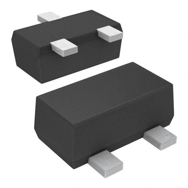
| 描述 | MOSFET N-CH 20V 1.73A 3UDFNMOSFET MOSFET BVDSS: 8V-24V X1-DFN1212-3,3K |
| 产品分类 | FET - 单分离式半导体 |
| FET功能 | 逻辑电平门 |
| FET类型 | MOSFET N 通道,金属氧化物 |
| Id-ContinuousDrainCurrent | 1.73 A |
| Id-连续漏极电流 | 1.73 A |
| 品牌 | Diodes Incorporated |
| 产品手册 | |
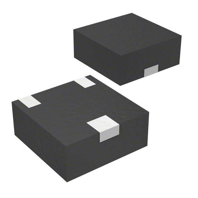
| 产品图片 |
|
| rohs | 符合RoHS无铅 / 符合限制有害物质指令(RoHS)规范要求 |
| 产品系列 | 晶体管,MOSFET,Diodes Incorporated DMN2300UFD-7- |
| 数据手册 | |
| 产品型号 | DMN2300UFD-7 |
| Pd-PowerDissipation | 0.96 W |
| Pd-功率耗散 | 960 mW |
| Qg-GateCharge | 2 nC |
| Qg-栅极电荷 | 2 nC |
| RdsOn-Drain-SourceResistance | 200 mOhms |
| RdsOn-漏源导通电阻 | 200 mOhms |
| RoHS指令信息 | http://diodes.com/download/4349 |
| Vds-Drain-SourceBreakdownVoltage | 20 V |
| Vds-漏源极击穿电压 | 20 V |
| Vgs-Gate-SourceBreakdownVoltage | +/- 8 V |
| Vgs-栅源极击穿电压 | 8 V |
| 上升时间 | 6.93 ns |
| 下降时间 | 10.62 ns |
| 不同Id时的Vgs(th)(最大值) | 950mV @ 250µA |
| 不同Vds时的输入电容(Ciss) | 67.62pF @ 25V |
| 不同Vgs时的栅极电荷(Qg) | 2nC @ 4.5V |
| 不同 Id、Vgs时的 RdsOn(最大值) | 200 毫欧 @ 900mA,4.5V |
| 产品种类 | MOSFET |
| 供应商器件封装 | X1-DFN1212-3 |
| 其它名称 | DMN2300UFD-7DITR |
| 典型关闭延迟时间 | 21.71 ns |
| 功率-最大值 | 470mW |
| 包装 | 带卷 (TR) |
| 商标 | Diodes Incorporated |
| 安装类型 | 表面贴装 |
| 安装风格 | SMD/SMT |
| 封装 | Reel |
| 封装/外壳 | 3-UDFN |
| 封装/箱体 | DFN1212-3 |
| 晶体管极性 | N-Channel |
| 最大工作温度 | + 150 C |
| 最小工作温度 | - 55 C |
| 标准包装 | 3,000 |
| 正向跨导-最小值 | 40 mS |
| 漏源极电压(Vdss) | 20V |
| 电流-连续漏极(Id)(25°C时) | 1.21A (Ta) |
| 系列 | DMN2300 |
| 通道模式 | Enhancement |
| 配置 | Single |


- 商务部:美国ITC正式对集成电路等产品启动337调查
- 曝三星4nm工艺存在良率问题 高通将骁龙8 Gen1或转产台积电
- 太阳诱电将投资9.5亿元在常州建新厂生产MLCC 预计2023年完工
- 英特尔发布欧洲新工厂建设计划 深化IDM 2.0 战略
- 台积电先进制程称霸业界 有大客户加持明年业绩稳了
- 达到5530亿美元!SIA预计今年全球半导体销售额将创下新高
- 英特尔拟将自动驾驶子公司Mobileye上市 估值或超500亿美元
- 三星加码芯片和SET,合并消费电子和移动部门,撤换高东真等 CEO
- 三星电子宣布重大人事变动 还合并消费电子和移动部门
- 海关总署:前11个月进口集成电路产品价值2.52万亿元 增长14.8%


PDF Datasheet 数据手册内容提取
A Product Line of Diodes Incorporated DMN2300UFD 20V N-CHANNEL ENHANCEMENT MODE MOSFET Product Summary Features and Benefits ID max • Low Gate Threshold Voltage V(BR)DSS RDS(on) Max TA = 25°C • Fast Switching Speed (Notes 4) • “Lead Free”, RoHS Compliant (Note 1) 200mΩ @ VGS = 4.5V 1.73A • Halogen and Antimony Free. "Green" Device (Note 2) 20V 260mΩ @ VGS = 2.5V 1.50A • ESD Protected Gate 2KV 400mΩ @ VGS = 1.8V 1.27A • Qualified to AEC-Q101 Standards for High Reliability 500mΩ @ VGS = 1.5V 1.15A Mechanical Data Description and Applications • Case: X1-DFN1212-3 This MOSFET has been designed to minimize the on-state resistance • Case Material: Molded Plastic, “Green” Molding Compound. (RDS(on)) and yet maintain superior switching performance, making it UL Flammability Classification Rating 94V-0 ideal for high efficiency power management applications. • Moisture Sensitivity: Level 1 per J-STD-020 • Terminals: Finish (cid:1755) NiPdAu over Copper leadframe. Solderable • Load switch per MIL-STD-202, Method 208 • Weight: 0.005 grams (approximate) Drain X1-DFN1212-3 Body Diode Gate Gate Protection Source Diode Top View Bottom View Equivalent Circuit Pin-out Top view Ordering Information (Note 3) Part Number Marking Reel size (inches) Tape width (mm) Quantity per reel DMN2300UFD-7 KS2 7 8 3000 Notes: 1. No purposefully added lead 2. Diodes Inc's "Green" policy can be found on our website at http://www.diodes.com. 3. For packaging details, go to our website at http://www.diodes.com. Marking Information KS2 = Product Type Marking Code YM = Date Code Marking Y = Year (ex: Y = 2011) M = Month (ex: 9 = September) Date Code Key Year 2011 2012 2013 2014 2015 2016 2017 Code Y Z A B C D E Month Jan Feb Mar Apr May Jun Jul Aug Sep Oct Nov Dec Code 1 2 3 4 5 6 7 8 9 O N D DMN2300UFD 1 of 7 September 2011 Datasheet Number: DS35443 Rev. 2 - 2 www.diodes.com © Diodes Incorporated
A Product Line of Diodes Incorporated DMN2300UFD Maximum Ratings @TA = 25°C unless otherwise specified Characteristic Symbol Value Unit Drain-Source Voltage VDSS 20 V Gate-Source Voltage VGSS ±8 V TA = 25°C (Note 4) 1.73 Steady Continuous Drain Current State TA = 85°C (Note 4) ID 1.34 A TA = 25°C (Note 5) 1.21 Pulsed Drain Current (Note 6) IDM 6.0 A Thermal Characteristics @TA = 25°C unless otherwise specified Characteristic Symbol Value Unit (Note 4) 0.96 W Power Dissipation (Note 5) PD 0.47 W (Note 4) 130 °C/W Thermal Resistance, Junction to Ambient (Note 5) RθJA 265 °C/W Operating and Storage Temperature Range TJ, TSTG -55 to +150 °C Notes: 4. For a device surface mounted on 15mm x 15mm x 1.6mm FR4 PCB with high coverage of 2oz copper, in still air conditions; the device is measured when operating in a steady-state condition. 5. Same as note 4, except the device is mounted on minimum recommended pad layout. 6. Device mounted on minimum recommended pad layout test board, 10µs pulse duty cycle = 1%. Thermal Characteristics 10 10 W) 9 SRiθnJgAl e= P1u3l6s°eC/W ID(A) @PW=1ms ID(A) RLiDmSit(eOdN) PEAK TRANSIENT POWER ( 345678 RTJθ J-A T (At) = = P R*RθJθAJA*r(t) I, DRAIN CURRENT (A)D 00.0.111 ID(AI) D(@A) D@CI P D(WA)=I 1D@(0AsP) W@=IP1sD(WA=)1 0@0PmsW=1@0PmWs=100µs k), 2 P(p 1 TTJA( M= A2X5)° =C 150°C ID(A) @ Single Pulse PW=10µs 0 0.001 0.00010.001 0.01 0.1 1 10 100 1000 0.1 1 10 100 t1, PULSE DURATION TIME (sec) VDS, DRAIN-SOURCE VOLTAGE (V) Fig. 1 Single Pulse Maximum Power Dissipation Fig. 2 SOA, Safe Operation Area DMN2300UFD 2 of 7 September 2011 Datasheet Number: DS35443 Rev. 2 - 2 www.diodes.com © Diodes Incorporated
A Product Line of Diodes Incorporated DMN2300UFD 1 CE D = 0.7 N D = 0.5 A T S D = 0.3 SI D = 0.9 E R AL 0.1 D = 0.1 M R E D = 0.05 H T T N D = 0.02 E NSI0.01 D = 0.01 A R r(t), T D = 0.005 RRDθθuJJtyAA (C=t) y 1=c3 lre6(,t° )CD */ W=R θt1JA/ t2 D = Single Pulse 0.001 0.000001 0.00001 0.0001 0.001 0.01 0.1 1 10 100 1,000 t1, PULSE DURATION TIMES (sec) Fig. 3 Transient Thermal Resistance Electrical Characteristics @TA = 25°C unless otherwise specified Characteristic Symbol Min Typ Max Unit Test Condition OFF CHARACTERISTICS (Note 7) Drain-Source Breakdown Voltage BVDSS 20 - - V VGS = 0V, ID = 250μA Zero Gate Voltage Drain Current TJ = 25°C IDSS - - 1 μA VDS = 20V, VGS = 0V Gate-Source Leakage IGSS - - ±10 μA VGS = ±8V, VDS = 0V ON CHARACTERISTICS (Note 7) Gate Threshold Voltage VGS(th) 0.45 - 0.95 V VDS = VGS, ID = 250μA 200 VGS = 4.5V, ID = 900mA Static Drain-Source On-Resistance RDS (ON) - - 246000 mΩ VVGGSS == 21..58VV,, IIDD == 870000mmAA 500 VGS = 1.5V, ID = 200mA Forward Transfer Admittance |Yfs| 40 - - mS VDS = 3V, ID = 300mA Diode Forward Voltage VSD - 0.7 1.2 V VGS = 0V, IS = 300mA DYNAMIC CHARACTERISTICS Input Capacitance Ciss - 67.62 - pF Output Capacitance Coss - 9.74 - pF fV =D S1 .=0 M25HVz, VGS = 0V, Reverse Transfer Capacitance Crss - 7.58 - pF Gate Resistance Rg - 68.51 - Ω VDS = 0V, VGS = 0V, f = 1MHz Total Gate Charge (Note 8) Qg - 0.89 2 nC GGaattee--SDorauirnc eC hCahragreg e QQggds -- 00..1164 -- nnCC IVDG =S 1=A 4 .5V, VDS = 15V, Turn-On Delay Time tD(on) - 4.92 - ns Turn-On Rise Time tr - 6.93 - ns VDS = 10V, ID = 1A Turn-Off Delay Time tD(off) - 21.71 - ns VGS = 10V, RG = 6Ω Turn-Off Fall Time tf - 10.62 - ns Notes: 7. Short duration pulse test used to minimize self-heating effect. 8. Guarantee by design. DMN2300UFD 3 of 7 September 2011 Datasheet Number: DS35443 Rev. 2 - 2 www.diodes.com © Diodes Incorporated
A Product Line of Diodes Incorporated DMN2300UFD 2.0 2.0 VGS = 4.5V VGS = 2.5V VDS = 5V VGS = 2.0V A) 1.5 VGS = 1.8V A) 1.5 NT ( VGS = 1.5V NT ( E E R R R R CU 1.0 CU 1.0 N N AI AI R R D D I, D 0.5 I, D 0.5 TA = 150°C TA = 125°C TA = 85°C VGS = 1.2V TA = 25°C TA = -55°C 0 0 0 1 2 3 4 5 0 0.5 1 1.5 2 2.5 3 V , DRAIN-SOURCE VOLTAGE (V) V , GATE-SOURCE VOLTAGE (V) DS GS Fig. 4 Typical Output Characteristic Fig. 5 Typical Transfer Characteristic 1 0.6 CE ()Ω VGS = 1.5V CE ()Ω 0.5 VGS = 4.5V N N A 0.8 A T T S S ESI ESI 0.4 R R N- 0.6 N- O O CE CE 0.3 TA = 125°C TA = 150°C R R SOU 0.4 VGS = 1.8V SOU 0.2 N- N- TA = 85°C RAI VGS = 2.5V RAI TA = 25°C D 0.2 D , ON) VGS = 4.5V , ON)0.1 TA = -55°C RDS( 0 RDS( 0 0 0.2 0.4 0.6 0.8 1 0 0.4 0.8 1.2 1.6 2 ID, DRAIN-SOURCE CURRENT (A) ID, DRAIN CURRENT (A) Fig. 6 Typical On-Resistance Fig. 7 Typical On-Resistance vs. Drain Current and Gate Voltage vs. Drain Current and Temperature 0.6 0.6 )Ω )Ω ANCE ( 0.5 VGS = 1.8V ANCE ( 0.5 VGS = 1.5V TA = 150°C TA = 125°C T T ESIS 0.4 TA = 125°C TA = 150°C ESIS 0.4 TA = 85°C N-R N-R TA = 25°C O O RCE 0.3 TA = 85°C RCE 0.3 TA = -55°C OU TA = 25°C OU S 0.2 S 0.2 N- N- RAI TA = -55°C RAI R, DDS(ON)0.10 R, DDS(ON)0.10 0 0.2 0.4 0.6 0.8 1 0 0.2 0.4 0.6 0.8 1 ID, DRAIN CURRENT (A) ID, DRAIN CURRENT (A) Fig. 8 Typical On-Resistance Fig. 9 Typical On-Resistance vs. Drain Current and Temperature vs. Drain Current and Temperature DMN2300UFD 4 of 7 September 2011 Datasheet Number: DS35443 Rev. 2 - 2 www.diodes.com © Diodes Incorporated
A Product Line of Diodes Incorporated DMN2300UFD 1.7 0.6 IVDG =S 5=0 20.m5VA E ()Ω D) 1.5 NC 0.5 R, DRAIN-SOURCE DSONRESISTANCE (NORMALIZE 011...913 VIGDS =V I=D G1 4.S=0. 5A=5V 01m.5AV IVDG =S 1=0 10.m8VA AIN-SOURCE ON-RESISTA 000...234 VIDG S= =5 01m.5AV IVDG =S 1=0 10.m8VA N- DR VGS = 4.5V O 0.7 , SON 0.1 IVDG =S 5=0 20.m5VA ID = 1.0A D R 0.5 0 -50 -25 0 25 50 75 100 125 150 -50 -25 0 25 50 75 100 125 150 T , AMBIENT TEMPERATURE (°C) T , AMBIENT TEMPERATURE (°C) A A Fig. 10 On-Resistance Variation with Temperature Fig. 11 On-Resistance Variation with Temperature 1.2 2.0 V) E ( 1.0 G 1.6 TA A) OL T ( V 0.8 ID = 1mA N OLD URRE 1.2 TA = 25°C ESH 0.6 ID = 250µA E C R C H R 0.8 T U E 0.4 O T S GA , S , H) 0.2 I 0.4 T S( G V 0 0 -50 -25 0 25 50 75 100 125 150 0 0.2 0.4 0.6 0.8 1.0 1.2 TA, AMBIENT TEMPERATURE (°C) VSD, SOURCE-DRAIN VOLTAGE (V) Fig. 12 Gate Threshold Variation vs. Ambient Temperature Fig. 13 Diode Forward Voltage vs. Current 1,000 100,000 TA = 125°C A) A) 10,000 RRENT (n 100 RRENT (n 1,000 TA = 125°C TA = 150°C U U E C TA = 85°C E C TA = 85°C G G KA KA 100 TA = 25°C I, LEADSS 10 TTAA == 2-555°°CC I, LEAGSS 10 TA = -55°C 1 1 2 4 6 8 10 12 14 16 18 20 2 4 6 8 10 12 V , DRAIN-SOURCE VOLTAGE (V) V , GATE-SOURCE VOLTAGE (V) DS GS Fig. 14 Typical Leakage Current Fig.15 Leakage Current vs. Gate-Source Voltage vs. Drain-Source Voltage DMN2300UFD 5 of 7 September 2011 Datasheet Number: DS35443 Rev. 2 - 2 www.diodes.com © Diodes Incorporated
A Product Line of Diodes Incorporated DMN2300UFD 8 V) GE ( 6 VDS = 15V A ID = 1A T L O V E C R 4 U O S E- T A G 2 , S G V 0 0 0.5 1 1.5 2 2.5 3 Q , TOTAL GATE CHARGE (nC) g Fig. 16 Gate-Charge Characteristics Package Outline Dimensions A X1-DFN1212-3 A3 Dim Min Max Typ A1 A 0.47 0.53 0.50 D A1 0 0.05 0.02 A3 - - 0.13 e b 0.27 0.37 0.32 b1 0.17 0.27 0.22 D 1.15 1.25 1.20 E 1.15 1.25 1.20 b1 e - - 0.80 E (2x) L 0.25 0.35 0.30 All Dimensions in mm L b Suggested Pad Layout X Y Dimensions Value (in mm) C 0.80 X 0.42 Y2 X1 X1 0.32 (2x) Y 0.50 Y1 Y1 0.50 (2x) Y2 1.50 C DMN2300UFD 6 of 7 September 2011 Datasheet Number: DS35443 Rev. 2 - 2 www.diodes.com © Diodes Incorporated
A Product Line of Diodes Incorporated DMN2300UFD MPORTANT NOTICE DIODES INCORPORATED MAKES NO WARRANTY OF ANY KIND, EXPRESS OR IMPLIED, WITH REGARDS TO THIS DOCUMENT, INCLUDING, BUT NOT LIMITED TO, THE IMPLIED WARRANTIES OF MERCHANTABILITY AND FITNESS FOR A PARTICULAR PURPOSE (AND THEIR EQUIVALENTS UNDER THE LAWS OF ANY JURISDICTION). Diodes Incorporated and its subsidiaries reserve the right to make modifications, enhancements, improvements, corrections or other changes without further notice to this document and any product described herein. Diodes Incorporated does not assume any liability arising out of the application or use of this document or any product described herein; neither does Diodes Incorporated convey any license under its patent or trademark rights, nor the rights of others. Any Customer or user of this document or products described herein in such applications shall assume all risks of such use and will agree to hold Diodes Incorporated and all the companies whose products are represented on Diodes Incorporated website, harmless against all damages. Diodes Incorporated does not warrant or accept any liability whatsoever in respect of any products purchased through unauthorized sales channel. Should Customers purchase or use Diodes Incorporated products for any unintended or unauthorized application, Customers shall indemnify and hold Diodes Incorporated and its representatives harmless against all claims, damages, expenses, and attorney fees arising out of, directly or indirectly, any claim of personal injury or death associated with such unintended or unauthorized application. Products described herein may be covered by one or more United States, international or foreign patents pending. Product names and markings noted herein may also be covered by one or more United States, international or foreign trademarks. LIFE SUPPORT Diodes Incorporated products are specifically not authorized for use as critical components in life support devices or systems without the express written approval of the Chief Executive Officer of Diodes Incorporated. As used herein: A. Life support devices or systems are devices or systems which: 1. are intended to implant into the body, or 2. support or sustain life and whose failure to perform when properly used in accordance with instructions for use provided in the labeling can be reasonably expected to result in significant injury to the user. B. A critical component is any component in a life support device or system whose failure to perform can be reasonably expected to cause the failure of the life support device or to affect its safety or effectiveness. Customers represent that they have all necessary expertise in the safety and regulatory ramifications of their life support devices or systems, and acknowledge and agree that they are solely responsible for all legal, regulatory and safety-related requirements concerning their products and any use of Diodes Incorporated products in such safety-critical, life support devices or systems, notwithstanding any devices- or systems-related information or support that may be provided by Diodes Incorporated. Further, Customers must fully indemnify Diodes Incorporated and its representatives against any damages arising out of the use of Diodes Incorporated products in such safety-critical, life support devices or systems. Copyright © 2011, Diodes Incorporated www.diodes.com DMN2300UFD 7 of 7 September 2011 Datasheet Number: DS35443 Rev. 2 - 2 www.diodes.com © Diodes Incorporated
Mouser Electronics Authorized Distributor Click to View Pricing, Inventory, Delivery & Lifecycle Information: D iodes Incorporated: DMN2300UFD-7