ICGOO在线商城 > 分立半导体产品 > 晶体管 - FET,MOSFET - 单 > AOTF18N65
 Datasheet下载
- 型号: AOTF18N65
- 制造商: ALPHA&OMEGA
- 库位|库存: xxxx|xxxx
- 要求:
| 数量阶梯 | 香港交货 | 国内含税 |
| +xxxx | $xxxx | ¥xxxx |
查看当月历史价格
查看今年历史价格
AOTF18N65产品简介:
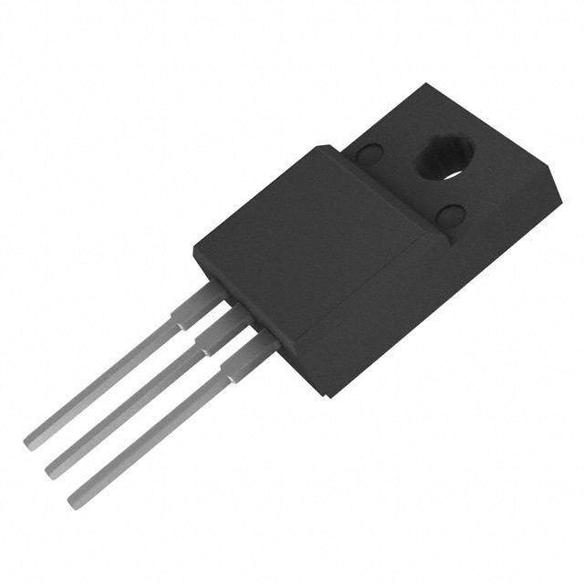
ICGOO电子元器件商城为您提供AOTF18N65由ALPHA&OMEGA设计生产,在icgoo商城现货销售,并且可以通过原厂、代理商等渠道进行代购。 AOTF18N65价格参考。ALPHA&OMEGAAOTF18N65封装/规格:晶体管 - FET,MOSFET - 单, 通孔 N 沟道 650V 18A(Tc) 50W(Tc) TO-220-3F。您可以下载AOTF18N65参考资料、Datasheet数据手册功能说明书,资料中有AOTF18N65 详细功能的应用电路图电压和使用方法及教程。
AOTF18N65 是 Alpha & Omega Semiconductor Inc. 生产的一款 N 沟道增强型 MOSFET,主要应用于电源管理和功率转换领域。该器件具有18A连续漏极电流和650V漏源击穿电压,适合中高功率应用。

主要应用场景包括:

1. 开关电源(SMPS):用于AC/DC转换器、DC/DC转换器等,具备高效率和低导通损耗,适合适配器、充电器、电源模块等设备。

2. 电机驱动:适用于电动工具、风扇、泵类等中小型电机控制电路,提供高效、可靠的开关性能。

3. 照明系统:如LED驱动电源、高压气体放电灯(HID)镇流器等,支持高频开关,提升能效。

4. 逆变器与UPS系统:用于不间断电源(UPS)或太阳能逆变器中,实现直流电到交流电的高效转换。

5. 工业自动化设备:在PLC、变频器、传感器供电模块中作为功率开关使用,具备良好的热稳定性和耐用性。

综上,AOTF18N65适用于需要高耐压、中等电流、高效率的功率电子设备,广泛用于工业、消费类及绿色能源领域。
| 参数 | 数值 |
| 产品目录 | |
| 描述 | MOSFET N-CH 600V 18A TO220F |
| 产品分类 | FET - 单 |
| FET功能 | 标准 |
| FET类型 | MOSFET N 通道,金属氧化物 |
| 品牌 | Alpha & Omega Semiconductor Inc |
| 数据手册 | |
| 产品图片 |
|
| 产品型号 | AOTF18N65 |
| rohs | 无铅 / 不符合限制有害物质指令(RoHS)规范要求 |
| 产品系列 | - |
| 不同Id时的Vgs(th)(最大值) | 4.5V @ 250µA |
| 不同Vds时的输入电容(Ciss) | 3785pF @ 25V |
| 不同Vgs时的栅极电荷(Qg) | 68nC @ 10V |
| 不同 Id、Vgs时的 RdsOn(最大值) | 390 毫欧 @ 9A,10V |
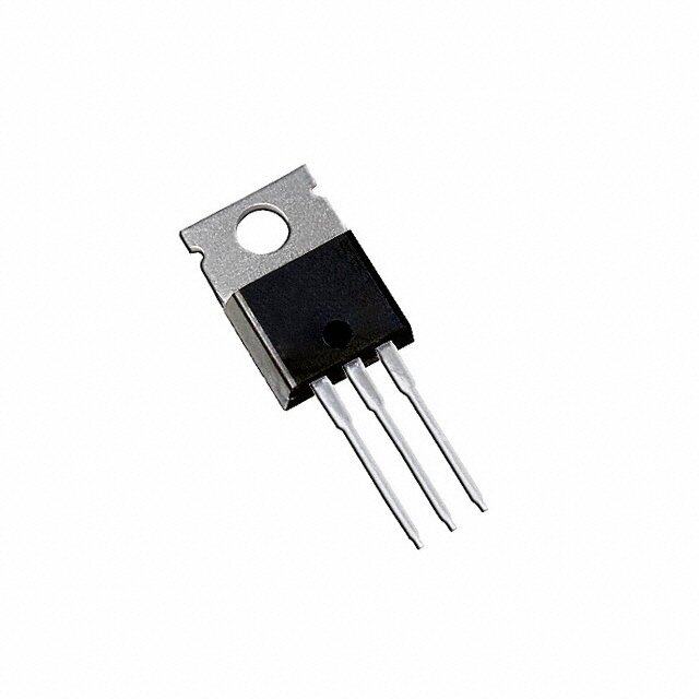
| 供应商器件封装 | TO-220F |
| 其它名称 | 785-1431-5 |
| 功率-最大值 | 50W |
| 包装 | 管件 |
| 安装类型 | 通孔 |
| 封装/外壳 | TO-220-3 整包 |
| 标准包装 | 50 |
| 漏源极电压(Vdss) | 650V |
| 电流-连续漏极(Id)(25°C时) | 18A (Tc) |


PDF Datasheet 数据手册内容提取
AOTF18N65 650V,18A N-Channel MOSFET General Description Product Summary The AOTF18N65 is fabricated using an advanced high VDS 750V@150℃ voltage MOSFET process that is designed to deliver high I (at V =10V) 18A D GS levels of performance and robustness in popular AC-DC R (at V =10V) < 0.39W DS(ON) GS applications.By providing low R , C and C along DS(on) iss rss with guaranteed avalanche capability this part can be adopted quickly into new and existing offline power supply designs. 100% UIS Tested 100% R Tested g For Halogen Free add "L" suffix to part number: AOTF18N65L Top View TO-220F D G D S S AOTF18N65 G Absolute Maximum Ratings T =25°C unless otherwise noted A Parameter Symbol AOTF18N65 Units Drain-Source Voltage V 650 V DS Gate-Source Voltage V ±30 V GS Continuous Drain TC=25°C I 18* Current T =100°C D 12* A C Pulsed Drain Current C I 80 DM Avalanche Current C I 6.3 A AR Repetitive avalanche energy C E 595 mJ AR Single pulsed avalanche energy G E 1190 mJ AS Peak diode recovery dv/dt dv/dt 5 V/ns T =25°C 50 W C P Power Dissipation B Derate above 25oC D 0.4 W/ oC Junction and Storage Temperature Range T, T -55 to 150 °C J STG Maximum lead temperature for soldering purpose, 1/8" from case for 5 seconds T 300 °C L Thermal Characteristics Parameter Symbol AOTF18N65 Units Maximum Junction-to-Ambient A,D RqJA 65 °C/W Maximum Junction-to-Case RqJC 2.5 °C/W * Drain current limited by maximum junction temperature. Rev0: Jul 2011 www.aosmd.com Page 1 of 5
AOTF18N65 Electrical Characteristics (T =25°C unless otherwise noted) J Symbol Parameter Conditions Min Typ Max Units STATIC PARAMETERS I =250µA, V =0V, T=25°C 650 BV Drain-Source Breakdown Voltage D GS J V DSS I =250µA, V =0V, T=150°C 750 D GS J BV Breakdown Voltage Temperature /∆TDJSS Coefficient ID=250µA, VGS=0V 0.7 V/ oC V =650V, V =0V 1 IDSS Zero Gate Voltage Drain Current VDS=520V, TG=S125°C 10 m A DS J I Gate-Body leakage current V =0V, V =±30V ±100 nA GSS DS GS V Gate Threshold Voltage V =5V, I =250m A 2.9 3.5 4.5 V GS(th) DS D R Static Drain-Source On-Resistance V =10V, I =9A 0.32 0.39 W DS(ON) GS D g Forward Transconductance V =40V, I =9A 20 S FS DS D V Diode Forward Voltage I =1A,V =0V 0.69 1 V SD S GS I Maximum Body-Diode Continuous Current* 18 A S I Maximum Body-Diode Pulsed Current 80 A SM DYNAMIC PARAMETERS C Input Capacitance 2270 3027 3785 pF iss C Output Capacitance V =0V, V =25V, f=1MHz 170 271 370 pF oss GS DS C Reverse Transfer Capacitance 12 22 32 pF rss R Gate resistance V =0V, V =0V, f=1MHz 0.7 1.4 2.1 W g GS DS SWITCHING PARAMETERS Q Total Gate Charge 44 56 68 nC g Q Gate Source Charge V =10V, V =520V, I =18A 9 12.4 15 nC gs GS DS D Q Gate Drain Charge 9 19.6 30 nC gd t Turn-On DelayTime 54 ns D(on) t Turn-On Rise Time V =10V, V =325V, I =18A, 83 ns r GS DS D ttDD((ooffff)) TTuurrnn--OOffff DDeellaayyTTiimmee RRGG==2255WW 114499 nnss t Turn-Off Fall Time 71 ns f trr Body Diode Reverse Recovery Time IF=18A,dI/dt=100A/m s,VDS=100V 520 655 790 ns Qrr Body Diode Reverse Recovery Charge IF=18A,dI/dt=100A/m s,VDS=100V 8 10 12 m C A. The value of RqJAis measured with the device in a still air environment with TA =25°C. B. The power dissipation P is based on T =150°C, using junction-to-case thermal resistance, and is more useful in setting the upper D J(MAX) dissipation limit for cases where additional heatsinking is used. C. Repetitive rating, pulse width limited by junction temperature T =150°C, Ratings are based on low frequency and duty cycles to keep initial J(MAX) T =25°C. J D. The RqJAis the sum of the thermal impedance from junction to case RqJCand case to ambient. E. The static characteristics in Figures 1 to 6 are obtained using <300 m s pulses, duty cycle 0.5% max. F. These curves are based on the junction-to-case thermal impedance which is measured with the device mounted to a large heatsink, assuming a maximum junction temperature of T =150°C. The SOA curve provides a single pulse rating. J(MAX) G. L=60mH, I =6.3A, V =150V, R =25Ω, Starting T=25°C AS DD G J THIS PRODUCT HAS BEEN DESIGNED AND QUALIFIED FOR THE CONSUMER MARKET. APPLICATIONS OR USES AS CRITICAL COMPONENTS IN LIFE SUPPORT DEVICES OR SYSTEMS ARE NOT AUTHORIZED. AOS DOES NOT ASSUME ANY LIABILITY ARISING OUT OF SUCH APPLICATIONS OR USES OF ITS PRODUCTS. AOS RESERVES THE RIGHT TO IMPROVE PRODUCT DESIGN, FUNCTIONS AND RELIABILITY WITHOUT NOTICE. Rev0: Jul 2011 www.aosmd.com Page 2 of 5
AOTF18N65 TYPICAL ELECTRICAL AND THERMAL CHARACTERISTICS 40 100 10V V =40V -55°C DS 30 6V 10 I(A)D 20 5.5V I(A)D 125°C 1 10 V =5V GS 25°C 0 0.1 0 5 10 15 20 25 30 0 2 4 6 8 10 Fig 1: On-RVeDgSio(nV oClthsa)racteristics Figure 2: TraVnGsSf(eVro Clths)aracteristics 0.6 3 0.5 VGS=10V stance 2.5 VIDG=S9=A10V si 2 e ) R W( n- N) 0.4 O 1.5 RDS(O alized 1 m 0.3 or N 0.5 0.2 0 0 10 20 30 40 -100 -50 0 50 100 150 200 I (A) Temperature (°C) Figure 3: On-ResistanceD vs. Drain Current and Gate Figure 4: On-Resistance vs. Junction Temperature VVoollttaaggee 1.2 1.0E+02 1.0E+01 ed) 1.1 1.0E4+000 z mali A) 125°C Nor 1 I(S 1.0E-01 ( SS 1.0E-02 25°C D V 0.9 B 1.0E-03 0.8 1.0E-04 -100 -50 0 50 100 150 200 0.0 0.2 0.4 0.6 0.8 1.0 TJ (°C) VSD(Volts) Figure 5:Break Down vs. Junction Temperature Figure 6: Body-Diode Characteristics (Note E) Rev0: Jul 2011 www.aosmd.com Page 3 of 5
AOTF18N65 TYPICAL ELECTRICAL AND THERMAL CHARACTERISTICS 15 10000 C iss V =520V 12 ID=S18A D F) 1000 p olts) 9 nce ( Coss V a (S cit VG 6 pa a 100 C C rss 3 0 10 0 20 40 60 80 100 0.1 1 10 100 Qg(nC) VDS(Volts) Figure 7: Gate-Charge Characteristics Figure 8: Capacitance Characteristics 20 100 10m s R DS(ON) limited A) 15 10 100m s (D g I ent ratin 10 (Amps)D 1 DC 110mmss urr I 0.1s C 5 0.1 1s T =150°C J(Max) T =25°C C 0 0.01 0 25 50 75 100 125 150 1 10 100 1000 TTCCAASSEE((°°CC)) VVDDSS((VVoollttss)) Figure 9: Current De-rating (Note B) Figure 10: Maximum Forward Biased Safe Operating Area for AOTF18N65 (Note F) 10 D=T /T In descending order on nsient nce 1 TRJq,JPCK==2T.C5+°PCDM/W.ZqJC.RqJC D=0.5, 0.3, 0.1, 0.05, 0.02, 0.01, single pulse Trasta d si ee malizmal R 0.1 PD Norher JCT 0.01 T Zq on T Single Pulse 0.001 0.00001 0.0001 0.001 0.01 0.1 1 10 100 Pulse Width (s) Figure 11: Normalized Maximum Transient Thermal Impedance for AOTF18N65 (Note F) Rev0: Jul 2011 www.aosmd.com Page 4 of 5
AOTF18N65 Gate Charge Test Circuit & Waveform Vgs Qg + 10V + VDC Qgs Qgd - Vds VDC - DUT Vgs Ig Charge Resistive Switching Test Circuit & Waveforms RL Vds Vds 90% + Vgs DUT Vdd VDC Rg - 10% Vgs Vgs td(on) tr td(off) tf ton toff Unclamped Inductive Switching (UIS) Test Circuit & Waveforms L 2 Vds E A R = 1/2 LI AR BVDSS Id Vds ++ VVggss Vgs VDC Vdd IAR Rg - Id DUT Vgs Vgs Diode Recovery Test Circuit & Waveforms Vds + Q r r = - Idt DUT Vgs Vds - L Isd I t Isd F dI/dt rr + I Vgs VDC Vdd RM Vdd - Vds Ig Rev0: Jul 2011 www.aosmd.com Page 5 of 5