ICGOO在线商城 > 分立半导体产品 > 晶体管 - 双极 (BJT) - 阵列 > ULN2803AFWG,C,EL
 Datasheet下载
- 型号: ULN2803AFWG,C,EL
- 制造商: Toshiba America Electronic Components, Inc.
- 库位|库存: xxxx|xxxx
- 要求:
| 数量阶梯 | 香港交货 | 国内含税 |
| +xxxx | $xxxx | ¥xxxx |
查看当月历史价格
查看今年历史价格
ULN2803AFWG,C,EL产品简介:
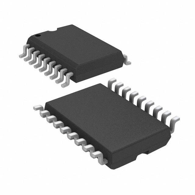
ICGOO电子元器件商城为您提供ULN2803AFWG,C,EL由Toshiba America Electronic Components, Inc.设计生产,在icgoo商城现货销售,并且可以通过原厂、代理商等渠道进行代购。 ULN2803AFWG,C,EL价格参考。Toshiba America Electronic Components, Inc.ULN2803AFWG,C,EL封装/规格:晶体管 - 双极 (BJT) - 阵列, Bipolar (BJT) Transistor Array 8 NPN Darlington 50V 500mA 1.31W Surface Mount 18-SOL。您可以下载ULN2803AFWG,C,EL参考资料、Datasheet数据手册功能说明书,资料中有ULN2803AFWG,C,EL 详细功能的应用电路图电压和使用方法及教程。
ULN2803AFWG,C,EL是东芝(Toshiba Semiconductor and Storage)生产的一款高耐压、大电流达林顿晶体管阵列,属于双极性晶体管(BJT)阵列类别。该器件内部集成了8组达林顿对管,每组均可承受高达50V的集电极电压和500mA的持续电流,具备较强的驱动能力。

该芯片广泛应用于需要驱动高负载的数字控制场景,典型应用包括:驱动继电器、步进电机或直流电机的控制电路;LED点阵显示屏的多路驱动;打印机、复印机等办公设备中的电磁阀或传感器驱动;工业自动化控制系统中的信号放大与隔离输出。由于其输入端兼容TTL和CMOS电平,可直接与微控制器(MCU)、FPGA或逻辑电路接口,简化了设计。

ULN2803AFWG,C,EL还内置了反向电动势保护二极管,特别适合驱动感性负载(如继电器、电机),有效防止关断时产生的高压反冲损坏前级电路。其小型化表面贴装封装(如SOP)形式,节省PCB空间,适用于紧凑型电子设备。

综上,该器件适用于各类中低频、中功率的开关与驱动场合,尤其在消费电子、工业控制、办公设备和家电控制模块中具有广泛应用价值。
| 参数 | 数值 |
| 产品目录 | |
| 描述 | TRANS 8 NPN DARL 50V 500MA 18SOL |
| 产品分类 | 晶体管(BJT) - 阵列 |
| 品牌 | Toshiba Semiconductor and Storage |
| 数据手册 | http://www.semicon.toshiba.co.jp/info/docget.jsp?pid=ULN2803APG&lang=en&type=datasheet |
| 产品图片 |
|
| 产品型号 | ULN2803AFWG,C,EL |
| rohs | 无铅 / 符合限制有害物质指令(RoHS)规范要求 |
| 产品系列 | - |
| 不同 Ib、Ic时的 Vce饱和值(最大值) | 1.6V @ 500µA, 350mA |
| 不同 Ic、Vce 时的DC电流增益(hFE)(最小值) | 1000 @ 350mA,2V |
| 供应商器件封装 | 18-SOL |
| 其它名称 | ULN2803AFWG(5ELMCT |
| 功率-最大值 | 1.31W |
| 包装 | 剪切带 (CT) |
| 安装类型 | 表面贴装 |
| 封装/外壳 | 18-SOIC(0.295",7.50mm 宽) |
| 晶体管类型 | 8 NPN 达林顿 |
| 标准包装 | 1 |
| 电压-集射极击穿(最大值) | 50V |
| 电流-集电极(Ic)(最大值) | 500mA |
| 电流-集电极截止(最大值) | - |
| 频率-跃迁 | - |


- 商务部:美国ITC正式对集成电路等产品启动337调查
- 曝三星4nm工艺存在良率问题 高通将骁龙8 Gen1或转产台积电
- 太阳诱电将投资9.5亿元在常州建新厂生产MLCC 预计2023年完工
- 英特尔发布欧洲新工厂建设计划 深化IDM 2.0 战略
- 台积电先进制程称霸业界 有大客户加持明年业绩稳了
- 达到5530亿美元!SIA预计今年全球半导体销售额将创下新高
- 英特尔拟将自动驾驶子公司Mobileye上市 估值或超500亿美元
- 三星加码芯片和SET,合并消费电子和移动部门,撤换高东真等 CEO
- 三星电子宣布重大人事变动 还合并消费电子和移动部门
- 海关总署:前11个月进口集成电路产品价值2.52万亿元 增长14.8%


PDF Datasheet 数据手册内容提取
ULN2803,04APG/AFWG TOSHIBA Bipolar Digital Integrated Circuit Silicon Monolithic ULN2803APG, ULN2803AFWG, ULN2804APG, ULN2804AFWG 8ch Darlington Sink Driver ULN2803APG The ULN2803APG / AFWG Series are high−voltage, ULN2804APG high−current darlington drivers comprised of eight NPN darlington pairs. All units feature integral clamp diodes for switching inductive loads. Applications include relay, hammer, lamp and display (LED) drivers. Features • Output current (single output) ULN2803AFWG 500 mA (max) ULN2804AFWG • High sustaining voltage output 50 V (min) • Output clamp diodes • Inputs compatible with various types of logic. • Package Type−APG : DIP−18pin • Package Type−AFWG : SOP−18pin Weight P-DIP18-300-2.54-001: 1.478 g (Typ.) P-SOP18-0812-1.27-001: 0.48 g (Typ.) Pin Connection (top view) Input Base Type Designation Resistor ULN2803APG / AFWG 2.7 kΩ TTL, 5 V CMOS ULN2804APG / AFWG 10.5 kΩ 6~15 V PMOS, CMOS 1 2012-11-26
ULN2803,04APG/AFWG Schematics (each driver) ULN2803APG / AFWG ULN2804APG / AFWG Note: The input and output parasitic diodes cannot be used as clamp diodes. Absolute Maximum Ratings (Ta = 25°C) Characteristic Symbol Rating Unit Output sustaining voltage VCE (SUS) −0.5 to 50 V Output current IOUT 500 mA / ch Input voltage VIN −0.5 to 30 V Clamp diode reverse voltage VR 50 V Clamp diode forward current IF 500 mA APG 1.47 Power dissipation PD W AFWG 0.92 / 1.31 (Note) Operating temperature Topr −40 to 85 °C Storage temperature Tstg −55 to 150 °C Note: On Glass Epoxy PCB (75 × 114 × 1.6 mm Cu 20%) 2 2012-11-26
ULN2803,04APG/AFWG Recommended Operating Conditions (Ta = −40~85°C) Characteristic Symbol Test Condition Min Typ. Max Unit Output sustaining voltage VCE (SUS) ― 0 ― 50 V tpw = 25 ms, Duty = 10%, 0 ― 347 8 Circuits APG tpw = 25 ms, Duty = 50%, 0 ― 123 8 Circuits mA / Output current IOUT ch tpw = 25 ms, Duty = 10%, 0 ― 268 8 Circuits AFWG tpw = 25 ms, Duty = 50%, 0 ― 90 8 Circuits Input voltage VIN ― 0 ― 30 V Input voltage ULN2803A ― 2.5 ― 30 (Output on) VIN (ON) V ULN2804A ― 8 ― 30 Clamp diode reverse voltage VR ― ― ― 50 V Clamp diode forward current IF ― ― ― 400 mA APG Ta = 85°C ― ― 0.76 Power dissipation PD W AFWG Ta = 85°C (Note) ― ― 0.48 Note: On Glass Epoxy PCB (75 × 114 × 1.6 mm Cu 20%) 3 2012-11-26
ULN2803,04APG/AFWG Electrical Characteristics (Ta = 25°C) Test Characteristic Symbol Cir− Test Condition Min Typ. Max Unit Cuit VCE = 50 V Ta = 25°C ― ― 50 Output leakage current ICEX 1 VCE = 50 V Ta = 85°C ― ― 100 μA ULN2804A VCE = 50 V VIN = 1 V ― ― 500 IOUT = 350 mA, IIN = 500 μA ― 1.3 1.6 Collector−emitter saturation voltage VCE (sat) 2 IOUT = 200 mA, IIN = 350 μA ― 1.1 1.3 V IOUT = 100 mA, IIN = 250 μA ― 0.9 1.1 ULN2803A VIN = 3.85 V ― 0.93 1.35 IIN (ON) 2 VIN = 5 V ― 0.35 0.5 mA Input current ULN2804A VIN = 12 V ― 1.0 1.45 IIN (OFF) 4 IOUT = 500 μA, Ta = 85°C 50 65 ― μA VCE = 2 V, IOUT = 200 mA ― ― 2.4 ULN2803A VCE = 2 V, IOUT = 250 mA ― ― 2.7 VCE = 2 V, IOUT = 300 mA ― ― 3.0 Input voltage (Output on) VIN (ON) 5 VCE = 2 V, IOUT = 125 mA ― ― 5.0 V VCE = 2 V, IOUT = 200 mA ― ― 6.0 ULN2804A VCE = 2 V, IOUT = 275 mA ― ― 7.0 VCE = 2 V, IOUT = 350 mA ― ― 8.0 DC current transfer ratio hFE 2 VCE = 2 V, IOUT = 350 mA 1000 ― ― ― Ta = 25°C (Note) ― ― 50 Clamp diode reverse current IR 6 μA Ta = 85°C (Note) ― ― 100 Clamp diode forward voltage VF 7 IF = 350 mA ― ― 2.0 V Input capacitance CIN ― ― ― 15 ― pF Turn−on delay tON RL = 125 Ω, VOUT = 50 V ― 0.1 ― 8 μs Turn−off delay tOFF RL = 125 Ω, VOUT = 50 V ― 0.2 ― Note: VR = VR (max) 4 2012-11-26
ULN2803,04APG/AFWG Test Circuit 1. I 2. V h 3. I CEX CE (sat), FE IN (ON) 4. I 5. V 6. I IN (OFF) IN (ON) R 7. V F 5 2012-11-26
ULN2803,04APG/AFWG 8. t , t ON OFF Note 1: Pulse Width 50 μs, Duty Cycle 10% Output Impedance 50 Ω, tr ≤ 5 ns, tf ≤ 10 ns Note 2: See below. Input Condition Type Number R1 VIH ULN2803A 0Ω 3 V ULN2804A 0Ω 8 V Note 3: CL includes probe and jig capacitance Precautions for Using This IC does not integrate protection circuits such as overcurrent and overvoltage protectors. Thus, if excess current or voltage is applied to the IC, the IC may be damaged. Please design the IC so that excess current or voltage will not be applied to the IC. Utmost care is necessary in the design of the output line, COMMON and GND line since IC may be destroyed due to short−circuit between outputs, air contamination fault, or fault by improper grounding. 6 2012-11-26
ULN2803,04APG/AFWG 7 2012-11-26
ULN2803,04APG/AFWG 8 2012-11-26
ULN2803,04APG/AFWG Package Dimensions P-DIP18-300-2.54-001 “Unit : mm” Weight: 1.478 g (typ.) This drawing is an object for explanation. 9 2012-11-26
ULN2803,04APG/AFWG Package Dimensions P-SOP18-0812-1.27-001 “Unit : mm” Weight: 0.48 g (typ.) This drawing is an object for explanation. 10 2012-11-26
ULN2803,04APG/AFWG Notes on Contents 1. Equivalent Circuits The equivalent circuit diagrams may be simplified or some parts of them may be omitted for explanatory purposes. 2. Test Circuits Components in the test circuits are used only to obtain and confirm the device characteristics. These components and circuits are not guaranteed to prevent malfunction or failure from occurring in the application equipment. IC Usage Considerations Notes on Handling of ICs (1) The absolute maximum ratings of a semiconductor device are a set of ratings that must not be exceeded, even for a moment. Do not exceed any of these ratings. Exceeding the rating(s) may cause the device breakdown, damage or deterioration, and may result injury by explosion or combustion. (2) Use an appropriate power supply fuse to ensure that a large current does not continuously flow in case of over current and/or IC failure. The IC will fully break down when used under conditions that exceed its absolute maximum ratings, when the wiring is routed improperly or when an abnormal pulse noise occurs from the wiring or load, causing a large current to continuously flow and the breakdown can lead smoke or ignition. To minimize the effects of the flow of a large current in case of breakdown, appropriate settings, such as fuse capacity, fusing time and insertion circuit location, are required. (3) If your design includes an inductive load such as a motor coil, incorporate a protection circuit into the design to prevent device malfunction or breakdown caused by the current resulting from the inrush current at power ON or the negative current resulting from the back electromotive force at power OFF. IC breakdown may cause injury, smoke or ignition. Use a stable power supply with ICs with built-in protection functions. If the power supply is unstable, the protection function may not operate, causing IC breakdown. IC breakdown may cause injury, smoke or ignition. (4) Do not insert devices in the wrong orientation or incorrectly. Make sure that the positive and negative terminals of power supplies are connected properly. Otherwise, the current or power consumption may exceed the absolute maximum rating, and exceeding the rating(s) may cause the device breakdown, damage or deterioration, and may result injury by explosion or combustion. In addition, do not use any device that is applied the current with inserting in the wrong orientation or incorrectly even just one time. (5) Carefully select external components (such as inputs and negative feedback capacitors) and load components (such as speakers), for example, power amp and regulator. If there is a large amount of leakage current such as input or negative feedback condenser, the IC output DC voltage will increase. If this output voltage is connected to a speaker with low input withstand voltage, overcurrent or IC failure can cause smoke or ignition. (The over current can cause smoke or ignition from the IC itself.) In particular, please pay attention when using a Bridge Tied Load (BTL) connection type IC that inputs output DC voltage to a speaker directly. 11 2012-11-26
ULN2803,04APG/AFWG Points to Remember on Handling of ICs (1) Heat Radiation Design In using an IC with large current flow such as power amp, regulator or driver, please design the device so that heat is appropriately radiated, not to exceed the specified junction temperature (Tj) at any time and condition. These ICs generate heat even during normal use. An inadequate IC heat radiation design can lead to decrease in IC life, deterioration of IC characteristics or IC breakdown. In addition, please design the device taking into considerate the effect of IC heat radiation with peripheral components. (2) Back-EMF When a motor rotates in the reverse direction, stops or slows down abruptly, a current flow back to the motor’s power supply due to the effect of back-EMF. If the current sink capability of the power supply is small, the device’s motor power supply and output pins might be exposed to conditions beyond absolute maximum ratings. To avoid this problem, take the effect of back-EMF into consideration in system design. About solderability, following conditions were confirmed • Solderability (1) Use of Sn-37Pb solder Bath · solder bath temperature = 230°C · dipping time = 5 seconds · the number of times = once · use of R-type flux (2) Use of Sn-3.0Ag-0.5Cu solder Bath · solder bath temperature = 245°C · dipping time = 5 seconds · the number of times = once · use of R-type flux 12 2012-11-26
ULN2803,04APG/AFWG RESTRICTIONS ON PRODUCT USE • Toshiba Corporation, and its subsidiaries and affiliates (collectively "TOSHIBA"), reserve the right to make changes to the information in this document, and related hardware, software and systems (collectively "Product") without notice. • This document and any information herein may not be reproduced without prior written permission from TOSHIBA. Even with TOSHIBA's written permission, reproduction is permissible only if reproduction is without alteration/omission. • Though TOSHIBA works continually to improve Product's quality and reliability, Product can malfunction or fail. Customers are responsible for complying with safety standards and for providing adequate designs and safeguards for their hardware, software and systems which minimize risk and avoid situations in which a malfunction or failure of Product could cause loss of human life, bodily injury or damage to property, including data loss or corruption. Before customers use the Product, create designs including the Product, or incorporate the Product into their own applications, customers must also refer to and comply with (a) the latest versions of all relevant TOSHIBA information, including without limitation, this document, the specifications, the data sheets and application notes for Product and the precautions and conditions set forth in the "TOSHIBA Semiconductor Reliability Handbook" and (b) the instructions for the application with which the Product will be used with or for. Customers are solely responsible for all aspects of their own product design or applications, including but not limited to (a) determining the appropriateness of the use of this Product in such design or applications; (b) evaluating and determining the applicability of any information contained in this document, or in charts, diagrams, programs, algorithms, sample application circuits, or any other referenced documents; and (c) validating all operating parameters for such designs and applications. TOSHIBA ASSUMES NO LIABILITY FOR CUSTOMERS' PRODUCT DESIGN OR APPLICATIONS. • PRODUCT IS NEITHER INTENDED NOR WARRANTED FOR USE IN EQUIPMENTS OR SYSTEMS THAT REQUIRE EXTRAORDINARILY HIGH LEVELS OF QUALITY AND/OR RELIABILITY, AND/OR A MALFUNCTION OR FAILURE OF WHICH MAY CAUSE LOSS OF HUMAN LIFE, BODILY INJURY, SERIOUS PROPERTY DAMAGE AND/OR SERIOUS PUBLIC IMPACT ("UNINTENDED USE"). Except for specific applications as expressly stated in this document, Unintended Use includes, without limitation, equipment used in nuclear facilities, equipment used in the aerospace industry, medical equipment, equipment used for automobiles, trains, ships and other transportation, traffic signaling equipment, equipment used to control combustions or explosions, safety devices, elevators and escalators, devices related to electric power, and equipment used in finance-related fields. IF YOU USE PRODUCT FOR UNINTENDED USE, TOSHIBA ASSUMES NO LIABILITY FOR PRODUCT. For details, please contact your TOSHIBA sales representative. • Do not disassemble, analyze, reverse-engineer, alter, modify, translate or copy Product, whether in whole or in part. • Product shall not be used for or incorporated into any products or systems whose manufacture, use, or sale is prohibited under any applicable laws or regulations. • The information contained herein is presented only as guidance for Product use. No responsibility is assumed by TOSHIBA for any infringement of patents or any other intellectual property rights of third parties that may result from the use of Product. No license to any intellectual property right is granted by this document, whether express or implied, by estoppel or otherwise. • ABSENT A WRITTEN SIGNED AGREEMENT, EXCEPT AS PROVIDED IN THE RELEVANT TERMS AND CONDITIONS OF SALE FOR PRODUCT, AND TO THE MAXIMUM EXTENT ALLOWABLE BY LAW, TOSHIBA (1) ASSUMES NO LIABILITY WHATSOEVER, INCLUDING WITHOUT LIMITATION, INDIRECT, CONSEQUENTIAL, SPECIAL, OR INCIDENTAL DAMAGES OR LOSS, INCLUDING WITHOUT LIMITATION, LOSS OF PROFITS, LOSS OF OPPORTUNITIES, BUSINESS INTERRUPTION AND LOSS OF DATA, AND (2) DISCLAIMS ANY AND ALL EXPRESS OR IMPLIED WARRANTIES AND CONDITIONS RELATED TO SALE, USE OF PRODUCT, OR INFORMATION, INCLUDING WARRANTIES OR CONDITIONS OF MERCHANTABILITY, FITNESS FOR A PARTICULAR PURPOSE, ACCURACY OF INFORMATION, OR NONINFRINGEMENT. • Do not use or otherwise make available Product or related software or technology for any military purposes, including without limitation, for the design, development, use, stockpiling or manufacturing of nuclear, chemical, or biological weapons or missile technology products (mass destruction weapons). Product and related software and technology may be controlled under the applicable export laws and regulations including, without limitation, the Japanese Foreign Exchange and Foreign Trade Law and the U.S. Export Administration Regulations. Export and re-export of Product or related software or technology are strictly prohibited except in compliance with all applicable export laws and regulations. • Please contact your TOSHIBA sales representative for details as to environmental matters such as the RoHS compatibility of Product. Please use Product in compliance with all applicable laws and regulations that regulate the inclusion or use of controlled substances, including without limitation, the EU RoHS Directive. TOSHIBA ASSUMES NO LIABILITY FOR DAMAGES OR LOSSES OCCURRING AS A RESULT OF NONCOMPLIANCE WITH APPLICABLE LAWS AND REGULATIONS. 13 2012-11-26