ICGOO在线商城 > 分立半导体产品 > 晶体管 - FET,MOSFET - 单 > SUM110P06-07L-E3
 Datasheet下载
- 型号: SUM110P06-07L-E3
- 制造商: Vishay
- 库位|库存: xxxx|xxxx
- 要求:
| 数量阶梯 | 香港交货 | 国内含税 |
| +xxxx | $xxxx | ¥xxxx |
查看当月历史价格
查看今年历史价格
SUM110P06-07L-E3产品简介:
ICGOO电子元器件商城为您提供SUM110P06-07L-E3由Vishay设计生产,在icgoo商城现货销售,并且可以通过原厂、代理商等渠道进行代购。 SUM110P06-07L-E3价格参考。VishaySUM110P06-07L-E3封装/规格:晶体管 - FET,MOSFET - 单, P-Channel 60V 110A (Tc) 3.75W (Ta), 375W (Tc) Surface Mount TO-263 (D2Pak)。您可以下载SUM110P06-07L-E3参考资料、Datasheet数据手册功能说明书,资料中有SUM110P06-07L-E3 详细功能的应用电路图电压和使用方法及教程。
Vishay Siliconix 的 SUM110P06-07L-E3 是一款 P 沟道增强型功率 MOSFET,采用先进的沟槽工艺制造,具有低导通电阻(RDS(on))和高效率的特点。该器件广泛应用于对空间和能效要求较高的电子设备中。

典型应用场景包括:便携式电子产品(如智能手机、平板电脑和笔记本电脑)中的电源管理与负载开关,用于电池供电系统的反向电流保护和电源切换;在DC-DC转换器中作为同步整流或高端/低端开关,提升转换效率;适用于热插拔控制器和过压保护电路,提供快速响应和可靠保护;还可用于电机驱动、LED驱动及各类工业控制模块中,实现高效、低功耗的开关控制。

由于其小型化封装(如PowerPAK SO-8),SUM110P06-07L-E3 特别适合高密度印刷电路板设计,节省空间的同时保持良好的散热性能。此外,该MOSFET符合RoHS环保标准,支持无铅焊接工艺,适用于消费类电子、通信设备和汽车电子等对可靠性要求较高的领域。

综上所述,SUM110P06-07L-E3 凭借其优异的电气性能和紧凑封装,是现代低电压、大电流开关应用中的理想选择。
| 参数 | 数值 |
| 产品目录 | |
| ChannelMode | Enhancement |
| 描述 | MOSFET P-CH 60V 110A D2PAKMOSFET 60V 110A 375W |
| 产品分类 | FET - 单分离式半导体 |
| FET功能 | 逻辑电平门 |
| FET类型 | MOSFET P 通道,金属氧化物 |
| Id-ContinuousDrainCurrent | 110 A |
| Id-连续漏极电流 | 110 A |
| 品牌 | Vishay / SiliconixVishay Siliconix |
| 产品手册 | |
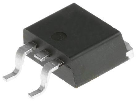
| 产品图片 |
|
| rohs | RoHS 合规性豁免无铅 / 符合限制有害物质指令(RoHS)规范要求 |
| 产品系列 | 晶体管,MOSFET,Vishay / Siliconix SUM110P06-07L-E3TrenchFET® |
| 数据手册 | |
| 产品型号 | SUM110P06-07L-E3SUM110P06-07L-E3 |
| Pd-PowerDissipation | 3.75 W |
| Pd-功率耗散 | 3.75 W |
| RdsOn-Drain-SourceResistance | 6.9 mOhms |
| RdsOn-漏源导通电阻 | 6.9 mOhms |
| Vds-Drain-SourceBreakdownVoltage | 60 V |
| Vds-漏源极击穿电压 | - 60 V |
| Vgs-Gate-SourceBreakdownVoltage | +/- 20 V |
| Vgs-栅源极击穿电压 | 20 V |
| 上升时间 | 160 ns |
| 下降时间 | 240 ns |
| 不同Id时的Vgs(th)(最大值) | 3V @ 250µA |
| 不同Vds时的输入电容(Ciss) | 11400pF @ 25V |
| 不同Vgs时的栅极电荷(Qg) | 345nC @ 10V |
| 不同 Id、Vgs时的 RdsOn(最大值) | 6.9 毫欧 @ 30A,10V |
| 产品目录页面 | |
| 产品种类 | MOSFET |
| 供应商器件封装 | TO-263(D2Pak) |
| 其它名称 | SUM110P06-07L-E3-ND |
| 典型关闭延迟时间 | 200 ns |
| 功率-最大值 | 3.75W |
| 包装 | 剪切带 (CT) |
| 商标 | Vishay / Siliconix |
| 商标名 | TrenchFET |
| 安装类型 | 表面贴装 |
| 安装风格 | SMD/SMT |
| 封装 | Reel |
| 封装/外壳 | TO-263-3,D²Pak(2 引线+接片),TO-263AB |
| 封装/箱体 | D2PAK-2 |
| 工厂包装数量 | 800 |
| 晶体管极性 | P-Channel |
| 最大工作温度 | + 175 C |
| 最小工作温度 | - 55 C |
| 标准包装 | 1 |
| 漏源极电压(Vdss) | 60V |
| 电流-连续漏极(Id)(25°C时) | 110A (Tc) |
| 系列 | SUM |
| 通道模式 | Enhancement |
| 配置 | Single |


- 商务部:美国ITC正式对集成电路等产品启动337调查
- 曝三星4nm工艺存在良率问题 高通将骁龙8 Gen1或转产台积电
- 太阳诱电将投资9.5亿元在常州建新厂生产MLCC 预计2023年完工
- 英特尔发布欧洲新工厂建设计划 深化IDM 2.0 战略
- 台积电先进制程称霸业界 有大客户加持明年业绩稳了
- 达到5530亿美元!SIA预计今年全球半导体销售额将创下新高
- 英特尔拟将自动驾驶子公司Mobileye上市 估值或超500亿美元
- 三星加码芯片和SET,合并消费电子和移动部门,撤换高东真等 CEO
- 三星电子宣布重大人事变动 还合并消费电子和移动部门
- 海关总署:前11个月进口集成电路产品价值2.52万亿元 增长14.8%


PDF Datasheet 数据手册内容提取
SUM110P06-07L www.vishay.com Vishay Siliconix P-Channel 60 V (D-S) 175 °C MOSFET FEATURES PRODUCT SUMMARY • TrenchFET® power MOSFET V (V) R (Ω) I (A) d DS DS(on) D • Package with low thermal resistance 0.0069 at V = -10 V GS -60 -110 • Material categorization: 0.0088 at V = -4.5 V GS for definitions of compliance please see www.vishay.com/doc?99912 S TO-263 G SS P-Channel MOSFET DD GG Top View D Ordering Information: SUM110P06-07L-E3 (Lead (Pb)-free) ABSOLUTE MAXIMUM RATINGS (T = 25 °C, unless otherwise noted) C PARAMETER SYMBOL LIMIT UNIT Drain-Source Voltage V -60 DS V Gate-Source Voltage V ± 20 GS Continuous Drain Current d TC = 25 °C -110 I (TJ = 175 °C) TC = 125 °C D -95 A Pulsed Drain Current I -240 DM Avalanche Current I -75 AS L = 0.1 mH Single Pulse Avalanche Energy a E 281 mJ AS T = 25 °C c 375 C Power Dissipation P W T = 25 °C b D 3.75 A Operating Junction and Storage Temperature Range T , T -55 to +175 °C J stg THERMAL RESISTANCE RATINGS PARAMETER SYMBOL TYPICAL UNIT Junction-to-Ambient PCB mount b R 40 thJA °C/W Junction-to-Case R 0.4 thJC Notes a. Duty cycle ≤ 1 %. b. When mounted on 1" square PCB (FR4 material). c. See SOA curve for voltage derating. d. Limited by package. S15-1278-Rev. D, 08-Jun-15 1 Document Number: 72439 For technical questions, contact: pmostechsupport@vishay.com THIS DOCUMENT IS SUBJECT TO CHANGE WITHOUT NOTICE. THE PRODUCTS DESCRIBED HEREIN AND THIS DOCUMENT ARE SUBJECT TO SPECIFIC DISCLAIMERS, SET FORTH AT www.vishay.com/doc?91000
SUM110P06-07L www.vishay.com Vishay Siliconix SPECIFICATIONS (T = 25 °C, unless otherwise noted) J PARAMETER SYMBOL TEST CONDITIONS MIN. TYP. MAX. UNIT Static Drain-Source Breakdown Voltage V V = 0 V, I = -250 μA -60 - - DS GS D V Gate Threshold Voltage V V = V , I = -250 μA -1 - -3 GS(th) DS GS D Gate-Body Leakage I V = 0 V, V = ± 20 V - - ± 100 nA GSS DS GS V = -60 V, V = 0 V - - -1 DS GS Zero Gate Voltage Drain Current I V = -60 V, V = 0 V, T = 125 °C - - -50 μA DSS DS GS J V = -60 V, V = 0 V, T = 175 °C - - -250 DS GS J On-State Drain Current a I V = -5 V, V = -10 V -120 - - A D(on) DS GS V = -10 V, I = -30 A - 0.0055 0.0069 GS D V = -10 V, I = -30 A, T = 125 °C - - 0.0115 Drain-Source On-State Resistance a R GS D J Ω DS(on) V = -10 V, I = -30 A, T = 175 °C - - 0.0138 GS D J V = -4.5 V, I = -20 A - 0.0070 0.0088 GS D Forward Transconductance a g V = -15 V, I = -50 A 20 - - S fs DS D Dynamic b Input Capacitance C - 11 400 - iss Output Capacitance C V = 0 V, V = -25 V, f = 1 MHz - 1200 - pF oss GS DS Reverse Transfer Capacitance C - 900 - rss Total Gate Charge c Q - 230 345 g Gate-Source Charge c Q V = -30 V, V = -10 V, I = -110 A - 50 - nC gs DS GS D Gate-Drain Charge c Q - 60 - gd Gate Resistance R f = 1 MHz - 3 - Ω g Turn-On Delay Time c t - 20 30 d(on) RTuisren -TOimff eD celay Time c tdt(orff) ID ≅ -1V1D0D A= ,- V3G0 EVN, =R L-1 =0 0V.2, 7R gΩ = 1 Ω -- 12150 24000 ns Fall Time c t - 50 100 f Drain-Source Body Diode Characteristics (T = 25 °C b) C Continuous Current I - - -110 S A Pulsed Current I - - -240 SM Forward Voltage a V I = -85 A, V = 0 V - -1 -1.5 V SD F GS Reverse Recovery Time t - 91 137 ns rr Peak Reverse Recovery Charge I I = -85 A, dI/dt = 100 A/μs - -6 -9 A RM(REC) F Reverse Recovery Charge Q - 0.21 0.44 μC rr Notes a. Pulse test; pulse width ≤ 300 μs, duty cycle ≤ 2 %. b. Guaranteed by design, not subject to production testing. c. Independent of operating temperature. Stresses beyond those listed under “Absolute Maximum Ratings” may cause permanent damage to the device. These are stress ratings only, and functional operation of the device at these or any other conditions beyond those indicated in the operational sections of the specifications is not implied. Exposure to absolute maximum rating conditions for extended periods may affect device reliability. S15-1278-Rev. D, 08-Jun-15 2 Document Number: 72439 For technical questions, contact: pmostechsupport@vishay.com THIS DOCUMENT IS SUBJECT TO CHANGE WITHOUT NOTICE. THE PRODUCTS DESCRIBED HEREIN AND THIS DOCUMENT ARE SUBJECT TO SPECIFIC DISCLAIMERS, SET FORTH AT www.vishay.com/doc?91000
SUM110P06-07L www.vishay.com Vishay Siliconix TYPICAL CHARACTERISTICS (25 °C, unless otherwise noted) 200 200 VGS = 10 V thru 5 V 160 160 urrent (A) 120 4 V Current (A) 120 - Drain CD 80 -I Drain D 80 TC = 125 °C I 40 40 25 °C 3 V -55 °C 0 0 0 2 4 6 8 10 0 1 2 3 4 5 VDS - Drain-to-Source Voltage (V) VGS - Gate-to-Source Voltage (V) Output Characteristics Transfer Characteristics 250 0.016 TC = -55 °C 0.014 200 ductance (S) 150 25 °C sistance () 00..001102 scon 125 °C n-Re 0.008 VGS = 4.5 V Tran 100 - O 0.006 - on) gfs DS( 0.004 VGS = 10 V 50 R 0.002 0 0.000 0 15 30 45 60 75 90 0 20 40 60 80 100 120 ID - Drain Current (A) ID - Drain Current (A) Transconductance On-Resistance vs. Drain Current 14 000 20 12 000 Ciss e (V) 16 IVDD =S 1=1 300 A V g e (pF)10 000 e Volta 12 c 8000 c citan Sour - CapaC 46000000 Gate-to- 8 Coss Crss -GS 4 2000 V 0 0 0 10 20 30 40 50 60 0 50 100 150 200 250 300 350 400 450 VDS - Drain-to-Source Voltage (V) Qg - Total Gate Charge (nC) Capacitance Gate Charge S15-1278-Rev. D, 08-Jun-15 3 Document Number: 72439 For technical questions, contact: pmostechsupport@vishay.com THIS DOCUMENT IS SUBJECT TO CHANGE WITHOUT NOTICE. THE PRODUCTS DESCRIBED HEREIN AND THIS DOCUMENT ARE SUBJECT TO SPECIFIC DISCLAIMERS, SET FORTH AT www.vishay.com/doc?91000
SUM110P06-07L www.vishay.com Vishay Siliconix TYPICAL CHARACTERISTICS (25 °C, unless otherwise noted) 2.0 75 VGS = 10 V ed) ID = 30 A ID = 250 µA z 1.7 72 ali m or N (ce 1.4 (V) 69 n S a S Resist 1.1 V(BR)D 66 n- O - on) 0.8 63 S( D R 0.5 60 -50 -25 0 25 50 75 100 125 150 175 -50 -25 0 25 50 75 100 125 150 175 TJ - Junction Temperature (°C) TJ - Junction Temperature (°C) On-Resistance vs. Junction Temperature Drain Source Breakdown vs. Junction Temperature 1000 200 100 150 A) Package Limited A) nt ( (DAV 10 IAV (A) at TA = 25 °C Curre 100 I n ai Dr - D 1 IAV (A) at TA = 150 °C I 50 0.1 0 0.00001 0.0001 0.001 0.01 0.1 1 0 25 50 75 100 125 150 175 tin (s) TC - Case Temperature (°C) Avalanche Current vs. Time Maximum Avalanche and Drain Current vs. Case Temperature 100 1000 Limited by R (DSon)* 10 µs 100 ent (A) nt (A) 100 µs ce Curr 10 TJ = 150 °C TJ = 25 °C n Curre 10 11 0m mss - SourIS - DraiID 1 100 ms, DC TC = 25 °C Single Pulse 1 0.1 0.0 0.3 0.6 0.9 1.2 0.1 1 10 100 VDS - Drain-to-Source Voltage (V) VSD - Source-to-Drain Voltage (V) * VGS minimum VGS at which RDS(on)isspecified Source-Drain Diode Forward Voltage Safe Operating Area S15-1278-Rev. D, 08-Jun-15 4 Document Number: 72439 For technical questions, contact: pmostechsupport@vishay.com THIS DOCUMENT IS SUBJECT TO CHANGE WITHOUT NOTICE. THE PRODUCTS DESCRIBED HEREIN AND THIS DOCUMENT ARE SUBJECT TO SPECIFIC DISCLAIMERS, SET FORTH AT www.vishay.com/doc?91000
SUM110P06-07L www.vishay.com Vishay Siliconix TYPICAL CHARACTERISTICS (25 °C, unless otherwise noted) 1 Duty Cycle = 0.5 nt 0.2 e e Transiedance 0.1 Notes: malized EffectivThermal Imp 0.1 Sin0g.0le02 .P0u5lse 1P. DDMuty Cyt1clet,2 D = tt12 Nor 23.. TPJe Mr U- TnAit =B aPsDeM =Z tRhJthAJ(At) = 62.5°C/W 4. Surface Mounted 0.01 10-4 10-3 10-2 10-1 1 Square Wave Pulse Duration (s) Normalized Thermal Transient Impedance, Junction-to-Case Vishay Siliconix maintains worldwide manufacturing capability. Products may be manufactured at one of several qualified locations. Reliability data for Silicon Technology and Package Reliability represent a composite of all qualified locations. For related documents such as package/tape drawings, part marking, and reliability data, see www.vishay.com/ppg?72439. S15-1278-Rev. D, 08-Jun-15 5 Document Number: 72439 For technical questions, contact: pmostechsupport@vishay.com THIS DOCUMENT IS SUBJECT TO CHANGE WITHOUT NOTICE. THE PRODUCTS DESCRIBED HEREIN AND THIS DOCUMENT ARE SUBJECT TO SPECIFIC DISCLAIMERS, SET FORTH AT www.vishay.com/doc?91000
Package Information www.vishay.com Vishay Siliconix TO-263 (D2PAK): 3-LEAD -B- A E c2 2 3 E1 6 -A- L 2D K D 4 D E3 1 D D L 3 L A A b2 c e b Detail “A” E2 0.010 M A M 2 PL 5° INCHES MILLIMETERS 0° - L4 DIM. MIN. MAX. MIN. MAX. A 0.160 0.190 4.064 4.826 b 0.020 0.039 0.508 0.990 L1 b1 0.020 0.035 0.508 0.889 b2 0.045 0.055 1.143 1.397 DETAIL A (ROTATED 90°) Thin lead 0.013 0.018 0.330 0.457 c* Thick lead 0.023 0.028 0.584 0.711 Thin lead 0.013 0.017 0.330 0.431 b c1 b1 Thick lead 0.023 0.027 0.584 0.685 M c2 0.045 0.055 1.143 1.397 c1 c D 0.340 0.380 8.636 9.652 SECTION A-A D1 0.220 0.240 5.588 6.096 D2 0.038 0.042 0.965 1.067 D3 0.045 0.055 1.143 1.397 D4 0.044 0.052 1.118 1.321 E 0.380 0.410 9.652 10.414 E1 0.245 - 6.223 - E2 0.355 0.375 9.017 9.525 E3 0.072 0.078 1.829 1.981 e 0.100 BSC 2.54 BSC K 0.045 0.055 1.143 1.397 Notes L 0.575 0.625 14.605 15.875 1. Plane B includes maximum features of heat sink tab and plastic. L1 0.090 0.110 2.286 2.794 2. No more than 25 % of L1 can fall above seating plane by L2 0.040 0.055 1.016 1.397 max. 8 mils. L3 0.050 0.070 1.270 1.778 3. Pin-to-pin coplanarity max. 4 mils. L4 0.010 BSC 0.254 BSC 4. *: Thin lead is for SUB, SYB. Thick lead is for SUM, SYM, SQM. M - 0.002 - 0.050 5. Use inches as the primary measurement. ECN: T13-0707-Rev. K, 30-Sep-13 6. This feature is for thick lead. DWG: 5843 Revison: 30-Sep-13 1 Document Number: 71198 THIS DOCUMENT IS SUBJECT TO CHANGE WITHOUT NOTICE. THE PRODUCTS DESCRIBED HEREIN AND THIS DOCUMENT ARE SUBJECT TO SPECIFIC DISCLAIMERS, SET FORTH AT www.vishay.com/doc?91000
AN826 Vishay Siliconix RECOMMENDED MINIMUM PADS FOR D2PAK: 3-Lead 0.420 (10.668) 5 7) 5 1 3 0 0. 9. ( 0.635 16.129) ( 0.145 (3.683) 0.135 (3.429) 0.200 0.050 (5.080) (1.257) Recommended Minimum Pads Dimensions in Inches/(mm) Return to Index Document Number: 73397 www.vishay.com 11-Apr-05 1
Legal Disclaimer Notice www.vishay.com Vishay Disclaimer ALL PRODUCT, PRODUCT SPECIFICATIONS AND DATA ARE SUBJECT TO CHANGE WITHOUT NOTICE TO IMPROVE RELIABILITY, FUNCTION OR DESIGN OR OTHERWISE. Vishay Intertechnology, Inc., its affiliates, agents, and employees, and all persons acting on its or their behalf (collectively, “Vishay”), disclaim any and all liability for any errors, inaccuracies or incompleteness contained in any datasheet or in any other disclosure relating to any product. Vishay makes no warranty, representation or guarantee regarding the suitability of the products for any particular purpose or the continuing production of any product. To the maximum extent permitted by applicable law, Vishay disclaims (i) any and all liability arising out of the application or use of any product, (ii) any and all liability, including without limitation special, consequential or incidental damages, and (iii) any and all implied warranties, including warranties of fitness for particular purpose, non-infringement and merchantability. Statements regarding the suitability of products for certain types of applications are based on Vishay’s knowledge of typical requirements that are often placed on Vishay products in generic applications. Such statements are not binding statements about the suitability of products for a particular application. It is the customer’s responsibility to validate that a particular product with the properties described in the product specification is suitable for use in a particular application. Parameters provided in datasheets and / or specifications may vary in different applications and performance may vary over time. All operating parameters, including typical parameters, must be validated for each customer application by the customer’s technical experts. Product specifications do not expand or otherwise modify Vishay’s terms and conditions of purchase, including but not limited to the warranty expressed therein. Except as expressly indicated in writing, Vishay products are not designed for use in medical, life-saving, or life-sustaining applications or for any other application in which the failure of the Vishay product could result in personal injury or death. Customers using or selling Vishay products not expressly indicated for use in such applications do so at their own risk. Please contact authorized Vishay personnel to obtain written terms and conditions regarding products designed for such applications. No license, express or implied, by estoppel or otherwise, to any intellectual property rights is granted by this document or by any conduct of Vishay. Product names and markings noted herein may be trademarks of their respective owners. © 2017 VISHAY INTERTECHNOLOGY, INC. ALL RIGHTS RESERVED Revision: 08-Feb-17 1 Document Number: 91000
Mouser Electronics Authorized Distributor Click to View Pricing, Inventory, Delivery & Lifecycle Information: V ishay: SUM110P06-07L-E3