ICGOO在线商城 > 分立半导体产品 > 晶体管 - FET,MOSFET - 单 > STP3NK60ZFP
 Datasheet下载
- 型号: STP3NK60ZFP
- 制造商: STMicroelectronics
- 库位|库存: xxxx|xxxx
- 要求:
| 数量阶梯 | 香港交货 | 国内含税 |
| +xxxx | $xxxx | ¥xxxx |
查看当月历史价格
查看今年历史价格
STP3NK60ZFP产品简介:
ICGOO电子元器件商城为您提供STP3NK60ZFP由STMicroelectronics设计生产,在icgoo商城现货销售,并且可以通过原厂、代理商等渠道进行代购。 STP3NK60ZFP价格参考。STMicroelectronicsSTP3NK60ZFP封装/规格:晶体管 - FET,MOSFET - 单, 通孔 N 沟道 600V 2.4A(Tc) 20W(Tc) TO-220FP。您可以下载STP3NK60ZFP参考资料、Datasheet数据手册功能说明书,资料中有STP3NK60ZFP 详细功能的应用电路图电压和使用方法及教程。
STP3NK60ZFP 是 STMicroelectronics(意法半导体)生产的一款 N 沟道增强型功率 MOSFET,属于晶体管 - FET,MOSFET - 单类别。以下是其主要应用场景:

 1. 开关电源 (SMPS)
   - STP3NK60ZFP 的高电压耐受能力(600V 额定电压)使其非常适合用于开关电源中的高压开关应用。
   - 常见于 AC-DC 转换器、适配器和充电器中,作为主开关器件。

 2. 电机驱动
   - 在小型电机驱动电路中,该 MOSFET 可用作开关元件,控制电机的启动、停止和速度调节。
   - 应用于家用电器(如风扇、泵)和工业设备中的电机控制。

 3. 逆变器
   - 用于太阳能逆变器或 UPS(不间断电源)系统中,作为高频开关元件,实现直流到交流的转换。
   - 其低导通电阻(Rds(on) = 0.95Ω @ Vgs=10V)有助于提高效率并减少功率损耗。

 4. 负载开关
   - 在需要高效负载切换的应用中,该 MOSFET 可用于开启或关闭负载电流,例如 LED 照明系统或电子镇流器。

 5. 保护电路
   - 由于其高击穿电压和良好的热稳定性,STP3NK60ZFP 可用于过流保护、短路保护和电子保险丝等电路中。

 6. 汽车电子
   - 在汽车电子领域,该 MOSFET 可用于车载充电器、电动车窗控制器和灯光控制系统中。
   - 特别适合需要承受高电压瞬态的环境。

 7. 家电与消费电子
   - 适用于各种家用电器(如洗衣机、空调、冰箱)和消费电子产品(如音响、显示器)中的电源管理和信号切换。

 总结
STP3NK60ZFP 凭借其高电压、低导通电阻和紧凑封装(TO-220FP),广泛应用于电力电子领域,尤其是在需要高效开关和高可靠性的工作环境中。
| 参数 | 数值 |
| 产品目录 | |
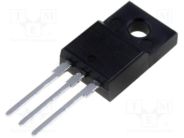
| 描述 | MOSFET N-CH 600V 2.4A TO-220FP |
| 产品分类 | FET - 单 |
| FET功能 | 标准 |
| FET类型 | MOSFET N 通道,金属氧化物 |
| 品牌 | STMicroelectronics |
| 数据手册 | |
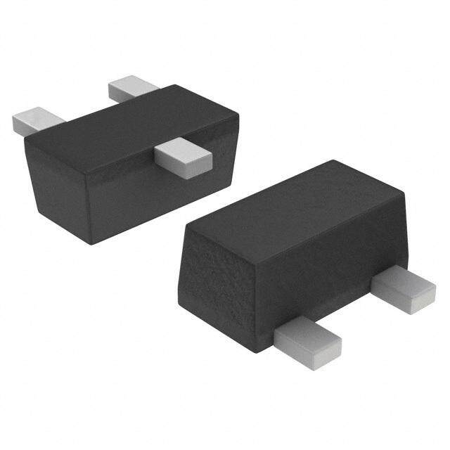
| 产品图片 |
|
| 产品型号 | STP3NK60ZFP |
| rohs | 无铅 / 符合限制有害物质指令(RoHS)规范要求 |
| 产品系列 | SuperMESH™ |
| 不同Id时的Vgs(th)(最大值) | 4.5V @ 50µA |
| 不同Vds时的输入电容(Ciss) | 311pF @ 25V |
| 不同Vgs时的栅极电荷(Qg) | 11.8nC @ 10V |
| 不同 Id、Vgs时的 RdsOn(最大值) | 3.6 欧姆 @ 1.2A,10V |
| 供应商器件封装 | TO-220FP |
| 其它名称 | 497-5978-5 |
| 其它有关文件 | http://www.st.com/web/catalog/sense_power/FM100/CL824/SC1167/PF223195?referrer=70071840 |
| 功率-最大值 | 20W |
| 包装 | 管件 |
| 安装类型 | 通孔 |
| 封装/外壳 | TO-220-3 整包 |
| 标准包装 | 50 |
| 漏源极电压(Vdss) | 600V |
| 电流-连续漏极(Id)(25°C时) | 2.4A (Tc) |


PDF Datasheet 数据手册内容提取
STP3NK60Z - STP3NK60ZFP STB3NK60Z-STD3NK60Z-STD3NK60Z-1 W N-CHANNEL 600V - 3.3 - 2.4A TO-220/FP/D2PAK/DPAK/IPAK Zener-Protected SuperMESH™Power MOSFET TYPE VDSS RDS(on) ID Pw STP3NK60Z 600V <3.6W 2.4A 45W STP3NK60ZFP 600V <3.6W 2.4A 20W STB3NK60Z 600V <3.6W 2.4A 45W STD3NK60Z 600V <3.6W 2.4A 45W STD3NK60Z-1 600V <3.6W 2.4A 45W 3 2 n TYPICALRDS(on)=3.3W TO-220 TO-220FP1 3 n EXTREMELY HIGHdv/dtCAPABILITY 1 n 100% AVALANCHE TESTED D2PAK GATECHARGE MINIMIZED n n VERYLOWINTRINSICCAPACITANCES 3 3 2 n VERYGOODMANUFACTURING 1 1 IPAK REPEATIBILITY DPAK DESCRIPTION The SuperMESH™ series is obtained through an INTERNALSCHEMATICDIAGRAM extreme optimization of ST’s well established strip- basedPowerMESH™layout.Inadditiontopushing on-resistancesignificantlydown,specialcareistak- en to ensure a very good dv/dt capability for the most demanding applications. Such series comple- ments ST full range of high voltage MOSFETs in- cludingrevolutionaryMDmesh™products. APPLICATIONS HIGHCURRENT,HIGHSPEEDSWITCHING n IDEALFOROFF-LINE POWERSUPPLIES, n ADAPTORS ANDPFC LIGHTING n ORDERINGINFORMATION SALESTYPE MARKING PACKAGE PACKAGING STP3NK60Z P3NK60Z TO-220 TUBE STP3NK60ZFP P3NK60ZFP TO-220FP TUBE STB3NK60ZT4 B3NK60Z D2PAK TAPE&REEL STD3NK60Z-1 D3NK60Z IPAK TUBE STD3NK60ZT4 D3NK60Z DPAK TAPE&REEL July2003 1/15
STP3NK60Z /FP - STB3NK60Z - STD3NK60Z - STD3NK60Z-1 ABSOLUTEMAXIMUMRATINGS Symbol Parameter Value Unit STP3NK60Z STD3NK60Z STP3NK60ZFP STB3NK60Z STD3NK60Z-1 VDS Drain-sourceVoltage(VGS=0) 600 V VDGR Drain-gateVoltage(RGS=20kW ) 600 V VGS Gate-sourceVoltage ±30 V ID DrainCurrent(continuous)atTC=25°C 2.4 2.4(*) 2.4(*) A ID DrainCurrent(continuous)atTC=100°C 1.51 1.51(*) 1.51(*) A IDM((cid:1)) DrainCurrent(pulsed) 9.6 9.6(*) 9.6(*) A PTOT TotalDissipationatTC=25°C 45 20 45 W DeratingFactor 0.36 0.16 0.36 W/°C VESD(G-S) GatesourceESD(HBM-C=100pF,R=1.5KW) 2100 V dv/dt(1) PeakDiodeRecoveryvoltageslope 4.5 V/ns VISO InsulationWithstandVoltage(DC) - 2500 - V Tj OperatingJunctionTemperature -55to150 °C Tstg StorageTemperature (cid:1) ( )Pulsewidthlimitedbysafeoperatingarea (1)ISD£ 2.4A,di/dt£ 200A/µs,VDD£ V(BR)DSS,Tj£ TJMAX. (*)Limitedonlybymaximumtemperatureallowed THERMALDATA TO-220 DPAK TO-220FP D2PAK IPAK Rthj-case ThermalResistanceJunction-caseMax 2.78 6.25 2.78 °C/W Rthj-amb ThermalResistanceJunction-ambientMax 62.5 100 °C/W Tl MaximumLeadTemperatureForSolderingPurpose 300 °C AVALANCHE CHARACTERISTICS Symbol Parameter MaxValue Unit IAR AvalancheCurrent,RepetitiveorNot-Repetitive 2.4 A (pulsewidthlimitedbyTjmax) EAS SinglePulseAvalancheEnergy 150 mJ (startingTj=25°C,ID=IAR,VDD=50V) GATE-SOURCEZENERDIODE Symbol Parameter TestConditions Min. Typ. Max. Unit BVGSO Gate-SourceBreakdown Igs=±1mA(OpenDrain) 30 V Voltage PROTECTIONFEATURESOFGATE-TO-SOURCE ZENERDIODES Thebuilt-inback-to-backZenerdiodeshavespecificallybeendesignedtoenhancenotonlythedevice’s ESDcapability,butalsotomakethemsafelyabsorbpossiblevoltagetransientsthatmayoccasionallybe appliedfromgatetosource.InthisrespecttheZenervoltageis appropriatetoachieveanefficientand cost-effectiveinterventiontoprotect thedevice’sintegrity.TheseintegratedZenerdiodes thusavoidthe usageofexternalcomponents. 2/15
STP3NK60Z /FP - STB3NK60Z - STD3NK60Z - STD3NK60Z-1 ELECTRICALCHARACTERISTICS (TCASE =25°CUNLESSOTHERWISESPECIFIED) ON/OFF Symbol Parameter TestConditions Min. Typ. Max. Unit V(BR)DSS Drain-source ID=1mA,VGS=0 600 V BreakdownVoltage IDSS ZeroGateVoltage VDS=MaxRating 1 µA DrainCurrent(VGS=0) VDS=MaxRating,TC=125°C 50 µA IGSS Gate-bodyLeakage VGS=±20V ±10 µA Current(VDS=0) VGS(th) GateThresholdVoltage VDS=VGS,ID=50µA 3 3.75 4.5 V RDS(on) StaticDrain-sourceOn VGS=10V,ID=1.2A 3.3 3.6 W Resistance DYNAMIC Symbol Parameter TestConditions Min. Typ. Max. Unit gfs(1) ForwardTransconductance VDS=20V,ID=1.2A 1.8 S Ciss InputCapacitance VDS=25V,f=1MHz,VGS=0 311 pF Coss OutputCapacitance 43 pF Crss ReverseTransfer 8 pF Capacitance Cosseq.(3) EquivalentOutput VGS=0,VDS=0to400V 26 pF Capacitance SWITCHINGON Symbol Parameter TestConditions Min. Typ. Max. Unit td(on) Turn-onDelayTime VDD=300V,ID=1.5A 9 ns tr RiseTime RG=4.7W VGS=10V 14 ns (ResistiveLoadsee,Figure3) Qg TotalGateCharge VDD=400V,ID=2.4A, 11.8 nC Qgs Gate-SourceCharge VGS=10V 2.6 nC Qgd Gate-DrainCharge 6.4 nC SWITCHINGOFF Symbol Parameter TestConditions Min. Typ. Max. Unit td(off) Turn-offDelayTime VDD=480V,ID=3A 19 ns tf FallTime RG=4.7W VGS=10V 14 ns (ResistiveLoadsee,Figure3) tr(Voff) Off-voltageRiseTime VDD=480V,ID=3A, 11 ns tf FallTime RG=4.7W, VGS=10V 14 ns tc Cross-overTime (InductiveLoadsee,Figure5) 24 ns SOURCEDRAINDIODE Symbol Parameter TestConditions Min. Typ. Max. Unit ISD Source-drainCurrent 2.4 A ISDM(2) Source-drainCurrent(pulsed) 9.6 A VSD(1) ForwardOnVoltage ISD=2.4A,VGS=0 1.6 V trr ReverseRecoveryTime ISD=3A,di/dt=100A/µs 306 ns Qrr ReverseRecoveryCharge VDD=35V,Tj=150°C 948 nC IRRM ReverseRecoveryCurrent (seetestcircuit,Figure5) 6.2 A Note: 1. Pulsed:Pulseduration=300µs,dutycycle1.5%. 2. Pulsewidthlimitedbysafeoperatingarea. 3. Cosseq.isdefinedasaconstantequivalentcapacitancegivingthesamechargingtimeasCosswhenVDSincreasesfrom0to80% VDSS. 3/15
STP3NK60Z /FP - STB3NK60Z - STD3NK60Z - STD3NK60Z-1 SafeOperatingArea ThermalImpedance SafeOperatingAreaForTO-220FP ThermalImpedanceForTO-220FP OutputCharacteristics TransferCharacteristics 4/15
STP3NK60Z /FP - STB3NK60Z - STD3NK60Z - STD3NK60Z-1 TTrraannssccoonndduuccttaannccee StaticDrain-sourceOn Resistance GateChargevsGate-sourceVoltage CapacitanceVariations NormalizedGateThresholdVoltagevsTemp. NormalizedOnResistancevsTemperature 5/15
STP3NK60Z /FP - STB3NK60Z - STD3NK60Z - STD3NK60Z-1 Source-drainDiodeForwardCharacteristics NormalizedBVDSS vsTemperature Maximum AvalancheEnergyvsTemperature 6/15
STP3NK60Z /FP - STB3NK60Z - STD3NK60Z - STD3NK60Z-1 Fig.1:UnclampedInductiveLoadTestCircuit Fig.2:UnclampedInductiveWaveform Fig.3:SwitchingTimes TestCircuitFor Fig.4:GateChargetestCircuit ResistiveLoad Fig.5:Test CircuitForInductiveLoadSwitching AndDiodeRecoveryTimes 7/15
STP3NK60Z /FP - STB3NK60Z - STD3NK60Z - STD3NK60Z-1 TO-220 MECHANICAL DATA mm inch DIM. MIN. TYP. MAX. MIN. TYP. MAX. A 4.40 4.60 0.173 0.181 C 1.23 1.32 0.048 0.051 D 2.40 2.72 0.094 0.107 D1 1.27 0.050 E 0.49 0.70 0.019 0.027 F 0.61 0.88 0.024 0.034 F1 1.14 1.70 0.044 0.067 F2 1.14 1.70 0.044 0.067 G 4.95 5.15 0.194 0.203 G1 2.4 2.7 0.094 0.106 H2 10.0 10.40 0.393 0.409 L2 16.4 0.645 L4 13.0 14.0 0.511 0.551 L5 2.65 2.95 0.104 0.116 L6 15.25 15.75 0.600 0.620 L7 6.2 6.6 0.244 0.260 L9 3.5 3.93 0.137 0.154 DIA. 3.75 3.85 0.147 0.151 E A C D 1 D L2 1 F 1 G 2 G H Dia. F 2 L5 F L9 L7 L6 L4 P011C 8/15
STP3NK60Z /FP - STB3NK60Z - STD3NK60Z - STD3NK60Z-1 TO-220FP MECHANICAL DATA mm. inch DIM. MIN. TYP MAX. MIN. TYP. MAX. A 4.4 4.6 0.173 0.181 B 2.5 2.7 0.098 0.106 D 2.5 2.75 0.098 0.108 E 0.45 0.7 0.017 0.027 F 0.75 1 0.030 0.039 F1 1.15 1.7 0.045 0.067 F2 1.15 1.7 0.045 0.067 G 4.95 5.2 0.195 0.204 G1 2.4 2.7 0.094 0.106 H 10 10.4 0.393 0.409 L2 16 0.630 L3 28.6 30.6 1.126 1.204 L4 9.8 10.6 .0385 0.417 L5 2.9 3.6 0.114 0.141 L6 15.9 16.4 0.626 0.645 L7 9 9.3 0.354 0.366 Ø 3 3.2 0.118 0.126 E A D B L3 L6 L7 1 ¯ F F 1 G H G 2 F 1 2 3 L5 L2 L4 9/15
STP3NK60Z /FP - STB3NK60Z - STD3NK60Z - STD3NK60Z-1 D2PAK MECHANICAL DATA mm. inch DIM. MIN. TYP MAX. MIN. TYP. MAX. A 4.4 4.6 0.173 0.181 A1 2.49 2.69 0.098 0.106 A2 0.03 0.23 0.001 0.009 B 0.7 0.93 0.027 0.036 B2 1.14 1.7 0.044 0.067 C 0.45 0.6 0.017 0.023 C2 1.23 1.36 0.048 0.053 D 8.95 9.35 0.352 0.368 D1 8 0.315 E 10 10.4 0.393 E1 8.5 0.334 G 4.88 5.28 0.192 0.208 L 15 15.85 0.590 0.625 L2 1.27 1.4 0.050 0.055 L3 1.4 1.75 0.055 0.068 M 2.4 3.2 0.094 0.126 R 0.4 0.015 V2 0º 4º 3 10/15 1
STP3NK60Z /FP - STB3NK60Z - STD3NK60Z - STD3NK60Z-1 TO-252 (DPAK) MECHANICAL DATA mm inch DIM. MIN. TYP. MAX. MIN. TYP. MAX. A 2.20 2.40 0.087 0.094 A1 0.90 1.10 0.035 0.043 A2 0.03 0.23 0.001 0.009 B 0.64 0.90 0.025 0.035 B2 5.20 5.40 0.204 0.213 C 0.45 0.60 0.018 0.024 C2 0.48 0.60 0.019 0.024 D 6.00 6.20 0.236 0.244 E 6.40 6.60 0.252 0.260 G 4.40 4.60 0.173 0.181 H 9.35 10.10 0.368 0.398 L2 0.8 0.031 L4 0.60 1.00 0.024 0.039 V2 0o 8o 0o 0o P032P_B 11/15
STP3NK60Z /FP - STB3NK60Z - STD3NK60Z - STD3NK60Z-1 TO-251 (IPAK) MECHANICAL DATA mm inch DIM. MIN. TYP. MAX. MIN. TYP. MAX. A 2.2 2.4 0.086 0.094 A1 0.9 1.1 0.035 0.043 A3 0.7 1.3 0.027 0.051 B 0.64 0.9 0.025 0.031 B2 5.2 5.4 0.204 0.212 B3 0.85 0.033 B5 0.3 0.012 B6 0.95 0.037 C 0.45 0.6 0.017 0.023 C2 0.48 0.6 0.019 0.023 D 6 6.2 0.236 0.244 E 6.4 6.6 0.252 0.260 G 4.4 4.6 0.173 0.181 H 15.9 16.3 0.626 0.641 L 9 9.4 0.354 0.370 L1 0.8 1.2 0.031 0.047 L2 0.8 1 0.031 0.039 H C A C2 A3 1 A L2 D L B3 B6 B B5 3 E = B2 = 2 G = = = = 1 L1 0068771-E 12/15
STP3NK60Z /FP - STB3NK60Z - STD3NK60Z - STD3NK60Z-1 DPAK FOOTPRINT TUBE SHIPMENT (no suffix)* All dimensions are in millimeters All dimensions are in millimeters TAPE AND REEL SHIPMENT (suffix ”T4”)* REEL MECHANICAL DATA mm inch DIM. MIN. MAX. MIN. MAX. A 330 12.992 B 1.5 0.059 C 12.8 13.2 0.504 0.520 D 20.2 0.795 G 16.4 18.4 0.645 0.724 N 50 1.968 T 22.4 0.881 BASE QTY BULKQTY TAPE MECHANICAL DATA 2500 2500 mm inch DIM. MIN. MAX. MIN. MAX. A0 6.8 7 0.267 0.275 B0 10.4 10.6 0.409 0.417 B1 12.1 0.476 D 1.5 1.6 0.059 0.063 D1 1.5 0.059 E 1.65 1.85 0.065 0.073 F 7.4 7.6 0.291 0.299 K0 2.55 2.75 0.100 0.108 P0 3.9 4.1 0.153 0.161 P1 7.9 8.1 0.311 0.319 P2 1.9 2.1 0.075 0.082 R 40 1.574 W 15.7 16.3 0.618 0.641 *onsalestype 13/15
STP3NK60Z /FP - STB3NK60Z - STD3NK60Z - STD3NK60Z-1 2 D PAK FOOTPRINT TUBE SHIPMENT (no suffix)* TAPE AND REEL SHIPMENT (suffix ”T4”)* REEL MECHANICAL DATA mm inch DIM. MIN. MAX. MIN. MAX. A 330 12.992 B 1.5 0.059 C 12.8 13.2 0.504 0.520 D 20.2 0795 G 24.4 26.4 0.960 1.039 N 100 3.937 T 30.4 1.197 BASE QTY BULKQTY TAPE MECHANICAL DATA 1000 1000 mm inch DIM. MIN. MAX. MIN. MAX. A0 10.5 10.7 0.413 0.421 B0 15.7 15.9 0.618 0.626 D 1.5 1.6 0.059 0.063 D1 1.59 1.61 0.062 0.063 E 1.65 1.85 0.065 0.073 F 11.4 11.6 0.449 0.456 K0 4.8 5.0 0.189 0.197 P0 3.9 4.1 0.153 0.161 P1 11.9 12.1 0.468 0.476 P2 1.9 2.1 0.075 0.082 R 50 1.574 T 0.25 0.35 0.0098 0.0137 W 23.7 24.3 0.933 0.956 14/15 *onsalestype
STP3NK60Z /FP - STB3NK60Z - STD3NK60Z - STD3NK60Z-1 Information furnished is believed to be accurate and reliable. However, STMicroelectronics assumes no responsibility for the consequences of use of such information nor for any infringement of patents or other rights of third parties which may result from its use. No license is granted by implication or otherwise under any patent or patent rights of STMicroelectronics. Specifications mentioned in this publication are subject to change without notice. This publication supersedes and replaces all information previously supplied. STMicroelectronics products are not authorized for use as critical components in life support devices or systems without express written approval of STMicroelectronics. © The ST logo is a registered trademark of STMicroelectronics © 2003 STMicroelectronics - Printed in Italy - All Rights Reserved STMicroelectronics GROUP OF COMPANIES Australia - Brazil - Canada - China - Finland - France - Germany - Hong Kong - India - Israel - Italy - Japan - Malaysia - Malta - Morocco Singapore - Spain - Sweden - Switzerland - United Kingdom - United States. © http://www.st.com 15/15
Mouser Electronics Authorized Distributor Click to View Pricing, Inventory, Delivery & Lifecycle Information: S TMicroelectronics: STP3NK60Z STD3NK60ZT4 STB3NK60ZT4 STP3NK60ZFP STD3NK60Z-1