ICGOO在线商城 > 分立半导体产品 > 晶体管 - FET,MOSFET - 单 > STW15N80K5
 Datasheet下载
- 型号: STW15N80K5
- 制造商: STMicroelectronics
- 库位|库存: xxxx|xxxx
- 要求:
| 数量阶梯 | 香港交货 | 国内含税 |
| +xxxx | $xxxx | ¥xxxx |
查看当月历史价格
查看今年历史价格
STW15N80K5产品简介:
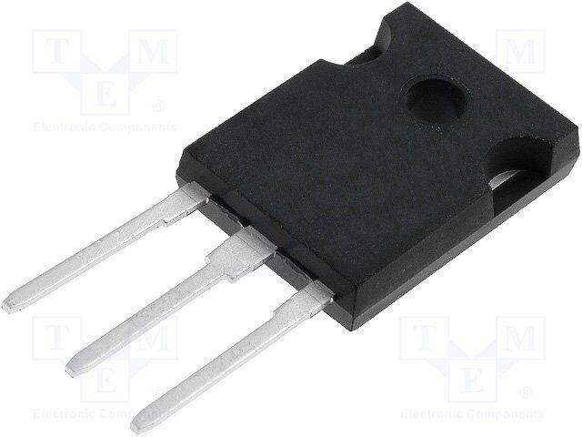
ICGOO电子元器件商城为您提供STW15N80K5由STMicroelectronics设计生产,在icgoo商城现货销售,并且可以通过原厂、代理商等渠道进行代购。 STW15N80K5价格参考¥31.82-¥31.82。STMicroelectronicsSTW15N80K5封装/规格:晶体管 - FET,MOSFET - 单, 通孔 N 沟道 800V 14A(Tc) 190W(Tc) TO-247。您可以下载STW15N80K5参考资料、Datasheet数据手册功能说明书,资料中有STW15N80K5 详细功能的应用电路图电压和使用方法及教程。
STMicroelectronics的STW15N80K5是一款高性能的N沟道增强型MOSFET,广泛应用于需要高效能功率转换的场景。其主要应用场景包括:

1. 电源管理:适用于开关电源(SMPS)、DC-DC转换器及AC-DC电源适配器,支持高效能与小型化设计。
2. 电机驱动:适合用于工业自动化设备、电动工具及家电中的电机控制模块,具备高耐压与低导通电阻特性,提升驱动效率。
3. 照明系统:应用于LED照明驱动电路,尤其在高亮度照明及智能照明控制中表现优异。
4. 新能源领域:如太阳能逆变器、储能系统等,支持高频率开关操作,减少能量损耗。
5. 汽车电子:用于车载充电系统、电池管理系统(BMS)或辅助电机控制,符合汽车级可靠性标准。

该器件具备800V高击穿电压、15A额定电流及低导通电阻(典型值0.38Ω),同时采用Housed TO-247封装,具备良好的热稳定性与耐用性,适合高功率密度与高效率要求的应用场景。
| 参数 | 数值 |
| 产品目录 | |
| 描述 | MOSFET N CH 800V 14A TO-247 |
| 产品分类 | FET - 单 |
| FET功能 | 标准 |
| FET类型 | MOSFET N 通道,金属氧化物 |
| 品牌 | STMicroelectronics |
| 数据手册 | |
| 产品图片 |
|
| 产品型号 | STW15N80K5 |
| rohs | 无铅 / 符合限制有害物质指令(RoHS)规范要求 |
| 产品系列 | SuperMESH5™ |
| 不同Id时的Vgs(th)(最大值) | 5V @ 100µA |
| 不同Vds时的输入电容(Ciss) | 1100pF @ 100V |
| 不同Vgs时的栅极电荷(Qg) | 32nC @ 10V |
| 不同 Id、Vgs时的 RdsOn(最大值) | 375 毫欧 @ 7A,10V |
| 供应商器件封装 | TO-247 |
| 其它名称 | 497-13447 |
| 其它有关文件 | http://www.st.com/web/catalog/sense_power/FM100/CL824/SC1168/PF254131?referrer=70071840 |
| 功率-最大值 | 190W |
| 包装 | 管件 |
| 安装类型 | 通孔 |
| 封装/外壳 | TO-247-3 |
| 标准包装 | 30 |
| 漏源极电压(Vdss) | 800V |
| 电流-连续漏极(Id)(25°C时) | 14A (Tc) |


.jpg)

- 商务部:美国ITC正式对集成电路等产品启动337调查
- 曝三星4nm工艺存在良率问题 高通将骁龙8 Gen1或转产台积电
- 太阳诱电将投资9.5亿元在常州建新厂生产MLCC 预计2023年完工
- 英特尔发布欧洲新工厂建设计划 深化IDM 2.0 战略
- 台积电先进制程称霸业界 有大客户加持明年业绩稳了
- 达到5530亿美元!SIA预计今年全球半导体销售额将创下新高
- 英特尔拟将自动驾驶子公司Mobileye上市 估值或超500亿美元
- 三星加码芯片和SET,合并消费电子和移动部门,撤换高东真等 CEO
- 三星电子宣布重大人事变动 还合并消费电子和移动部门
- 海关总署:前11个月进口集成电路产品价值2.52万亿元 增长14.8%


PDF Datasheet 数据手册内容提取
STB15N80K5, STF15N80K5, STP15N80K5, STW15N80K5 Ω N-channel 800 V, 0.3 typ., 14 A MDmesh™ K5 Power MOSFETs 2 in D PAK, TO-220FP, TO-220 and TO-247 packages − Datasheet production data Features TAB Order code V R max I P DS DS(on) D TOT 3 STB15N80K5 190 W 1 D2PAK 23 STF15N80K5 35 W 1 800 V 0.375 Ω 14 A TO-220FP STP15N80K5 190 W TAB STW15N80K5 • Industry’s lowest R x area DS(on) • Industry’s best figure of merit (FoM) 3 1 2 2 3 • Ultra low gate charge 1 TO-220 TO-247 • 100% avalanche tested • Zener-protected Figure 1. Internal schematic diagram D(2, TAB) Applications • Switching applications Description G(1) These very high voltage N-channel Power MOSFETs are designed using MDmesh™ K5 technology based on an innovative proprietary vertical structure. The result is a dramatic reduction in on-resistance and ultra-low gate charge for applications requiring superior power S(3) density and high efficiency. AM01476v1 Table 1. Device summary Order code Marking Package Packaging STB15N80K5 D2PAK Tape and reel STF15N80K5 TO-220FP 15N80K5 STP15N80K5 TO-220 Tube STW15N80K5 TO-247 October 2014 DocID023468 Rev 3 1/23 This is information on a product in full production. www.st.com 23
Contents STB15N80K5, STF15N80K5, STP15N80K5, STW15N80K5 Contents 1 Electrical ratings . . . . . . . . . . . . . . . . . . . . . . . . . . . . . . . . . . . . . . . . . . . . 3 2 Electrical characteristics . . . . . . . . . . . . . . . . . . . . . . . . . . . . . . . . . . . . . 4 2.1 Electrical characteristics (curves) . . . . . . . . . . . . . . . . . . . . . . . . . . . . . . . . 6 3 Test circuits . . . . . . . . . . . . . . . . . . . . . . . . . . . . . . . . . . . . . . . . . . . . . . 9 4 Package mechanical data . . . . . . . . . . . . . . . . . . . . . . . . . . . . . . . . . . . . 10 4.1 STB15N80K5, D²PAK (TO-263) . . . . . . . . . . . . . . . . . . . . . . . . . . . . . . . . .11 4.2 STP15N80K5, TO-220 . . . . . . . . . . . . . . . . . . . . . . . . . . . . . . . . . . . . . . . 14 4.3 STF15N80K5, TO-220FP . . . . . . . . . . . . . . . . . . . . . . . . . . . . . . . . . . . . . 16 4.4 STW15N80K5, TO-247 . . . . . . . . . . . . . . . . . . . . . . . . . . . . . . . . . . . . . . 18 5 Packaging information . . . . . . . . . . . . . . . . . . . . . . . . . . . . . . . . . . . . . . 20 6 Revision history . . . . . . . . . . . . . . . . . . . . . . . . . . . . . . . . . . . . . . . . . . . 22 2/23 DocID023468 Rev 3
STB15N80K5, STF15N80K5, STP15N80K5, STW15N80K5 Electrical ratings 1 Electrical ratings Table 2. Absolute maximum ratings Value Symbol Parameter D2PAK, Unit TO-220FP TO-220, TO-247 V Gate- source voltage ± 30 V GS I Drain current (continuous) at T = 25 °C 14 14(1) A D C I Drain current (continuous) at T = 100 °C 8.8 8.8 (1) A D C I (2) Drain current (pulsed) 56 56 (1) A DM P Total dissipation at T = 25 °C 190 35 W TOT C Max current during repetitive or single I pulse avalanche 4 A AR (pulse width limited by T ) jmax Single pulse avalanche energy E 150 mJ AS (starting T = 25 °C, I =I , V = 50 V) J D AS DD Insulation withstand voltage (RMS) from V all three leads to external heat sink 2500 V iso (t=1 s;T =25 °C) C dv/dt (3) Peak diode recovery voltage slope 4.5 V/ns T Operating junction temperature j -55 to 150 °C T Storage temperature stg 1. Limited by package. 2. Pulse width limited by safe operating area. 3. I ≤ 14 A, di/dt ≤ 100 A/µs, V ≤ V SD Peak (BR)DSS Table 3. Thermal data Value Symbol Parameter Unit TO-220 TO-247 D2PAK TO-220FP Thermal resistance junction-case R 0.66 3.6 thj-case max °C/W R Thermal resistance junction-amb max 62.5 50 62.5 thj-amb R (1) Thermal resistance junction-pcb max 30 thj-pcb 1. When mounted on 1inch² FR-4 board, 2 oz Cu. DocID023468 Rev 3 3/23
Electrical characteristics STB15N80K5, STF15N80K5, STP15N80K5, STW15N80K5 2 Electrical characteristics (T = 25 °C unless otherwise specified). CASE Table 4. On/off states Symbol Parameter Test conditions Min. Typ. Max. Unit Drain-source breakdown V I = 1 mA 800 V (BR)DSS voltage (V = 0) D GS Zero gate voltage drain VDS = 800 V 1 µA I DSS current (VGS = 0) VDS = 800 V, Tc=125 °C 50 µA Gate body leakage current I V = ± 20 V ±10 µA GSS (V = 0) GS DS V Gate threshold voltage V = V , I = 100 µA 3 4 5 V GS(th) DS GS D Static drain-source on R V = 10 V, I = 7 A 0.3 0.375 Ω DS(on) resistance GS D Table 5. Dynamic Symbol Parameter Test conditions Min. Typ. Max. Unit C Input capacitance - 1100 - pF iss C Output capacitance - 85 - pF oss V =100 V, f=1 MHz, V =0 DS GS Reverse transfer C - 1.5 - pF rss capacitance Equivalent capacitance time C (1) - 113 - pF o(tr) related V = 0, V = 0 to 640 V GS DS Equivalent capacitance C (2) - 49 - pF o(er) energy related R Intrinsic gate resistance f = 1MHz, I =0 - 4.5 - Ω G D Q Total gate charge - 32 - nC g V = 640 V, I = 14 A DD D Q Gate-source charge V =10 V - 6 - nC gs GS (see Figure20) Q Gate-drain charge - 22 - nC gd 1. Time related is defined as a constant equivalent capacitance giving the same charging time as C when oss V increases from 0 to 80% V DS DSS 2. Energy related is defined as a constant equivalent capacitance giving the same stored energy as C oss when V increases from 0 to 80% V DS DSS 4/23 DocID023468 Rev 3
STB15N80K5, STF15N80K5, STP15N80K5, STW15N80K5 Electrical characteristics Table 6. Switching times Symbol Parameter Test conditions Min. Typ. Max. Unit t Turn-on delay time - 19 - ns d(on) V = 400 V, I = 7 A, t Rise time DD D - 17.6 - ns r R =4.7 Ω, V =10 V G GS t Turn-off delay time - 44 - ns d(off) (see Figure19 and 24) t Fall time - 10 - ns f Table 7. Source drain diode Symbol Parameter Test conditions Min. Typ. Max. Unit I Source-drain current - 14 A SD I Source-drain current (pulsed) - 56 A SDM V (1) Forward on voltage I = 14 A, V =0 - 1.5 V SD SD GS t Reverse recovery time - 445 ns rr I = 14 A, V = 60 V SD DD Q Reverse recovery charge di/dt = 100 A/µs, - 8.2 μC rr (see Figure21) I Reverse recovery current - 37 A RRM t Reverse recovery time I = 14 A,V = 60 V - 580 ns rr SD DD Q Reverse recovery charge di/dt=100 A/µs, - 10 μC rr Tj=150 °C I Reverse recovery current (see Figure21) - 35 A RRM 1. Pulsed: pulse duration = 300µs, duty cycle 1.5% Table 8. Gate-source Zener diode Symbol Parameter Test conditions Min. Typ. Max Unit V Gate-source breakdown voltage I = ± 1mA, I = 0 30 - - V (BR)GSO GS D The built-in back-to-back Zener diodes have been specifically designed to enhance the ESD capability of the device. The Zener voltage is appropriate for efficient and cost-effective intervention to protect the device integrity. These integrated Zener diodes thus eliminate the need for external components. DocID023468 Rev 3 5/23
Electrical characteristics STB15N80K5, STF15N80K5, STP15N80K5, STW15N80K5 2.1 Electrical characteristics (curves) Figure 2. Safe operating area for D2PAK and Figure 3. Thermal impedance for D2PAK and TO-220 TO-220 ID AM15432v1 (A) 1µs 101 OperLiatimiotne id n btyh ism aarx eaR iDsS(on) Tj=150°C 111100m0µm0ssµss Tc=25°C Single pulse 0.1 0.1 1 10 100 VDS(V) Figure 4. Safe operating area for TO-220FP Figure 5. Thermal impedance for TO-220FP ID AM15433v1 (A) 1µs 101 OpeLriatmiitoen di nb ty hims aaxr eRa DiSs(on) 11100m0µsµss 10ms Tj=150°C 0.1 Tc=25°C Single pulse 0.01 0.1 1 10 100 VDS(V) Figure 6 . Safe operating area for TO-247 Figure 7. Thermal impedance for TO-247 ID AM15434v1 (A) 1µs 10µs 10 Operatimiotne id n btyh ism aarx eaR iDsS(on) 11100m0msµss 1 Li Tj=150°C Tc=25°C Single pulse 0.1 0.1 1 10 100 VDS(V) 6/23 DocID023468 Rev 3
STB15N80K5, STF15N80K5, STP15N80K5, STW15N80K5 Electrical characteristics Figure 8. Output characteristics Figure 9. Transfer characteristics AM15435v1 AM15436v1 ID ID (A) (A) VGS= 10 V 30 30 VDS= 20 V VGS= 9 V 24 24 VGS= 8 V 18 18 12 VGS= 7 V 12 6 6 VGS= 6 V 0 0 0 4 8 12 16 VDS(V) 4 6 8 10 VGS(V) Figure 10. Gate charge vs gate-source voltage Figure 11. Static drain-source on-resistance VGS AMV1D54S43v1 RDS(Ω(on)) AM15441v1 (V) VDD=640 V (V) 12 VDS ID=14 A 600 0.5 VGS=10V 10 500 0.4 8 400 0.3 6 300 0.2 4 200 2 100 0.1 0 0 0 0 5 10 15 20 25 30 Qg(nC) 0 5 10 15 20 25 ID(A) Figure 12. Capacitance variations Figure 13. Source-drain diode forward characteristics C AM15442v1 VSD AM15439v1 (pF) (V) T J=-50°C 1000 Ciss 0.9 TJ=25°C 100 0.8 Coss 10 0.7 Crss TJ=150°C 1 0.6 0.1 1 10 100 VDS(V) 4 6 8 10 12 ISD(A) DocID023468 Rev 3 7/23
Electrical characteristics STB15N80K5, STF15N80K5, STP15N80K5, STW15N80K5 Figure 14. Normalized gate threshold voltage vs Figure 15. Normalized on-resistance vs temperature temperature VGS(th) AM15440v1 RDS(on) AM15437v1 (norm) VDS = VGS (norm) VGS = 10 V 1.1 ID = 100 µA ID = 7 A 2.4 1 2 0.9 1.6 0.8 1.2 0.7 0.6 0.8 0.5 0.4 -75 -25 25 75 125 TJ(°C) -75 -25 25 75 125 TJ(°C) Figure 16. Output capacitance stored energy Figure 17. Normalized V vs temperature DS Eoss AM15444v1 VDS AM15438v1 (µJ) (norm) 1.1 ID = 1mA 12 1.06 8 1.02 0.98 4 0.94 0 0.9 0 200 400 600 VDS(V) -75 -25 25 75 125TJ(°C) Figure 18 . Maximum avalanche energy vs temperature (cid:40)(cid:36)(cid:54) (cid:36)(cid:48)(cid:20)(cid:24)(cid:23)(cid:23)(cid:24)(cid:89)(cid:20) (cid:11)(cid:80)(cid:45)(cid:12) (cid:44)(cid:39)(cid:32)(cid:23)(cid:3)(cid:36) (cid:20)(cid:21)(cid:19) (cid:57)(cid:39)(cid:39)(cid:32)(cid:24)(cid:19)(cid:3)(cid:57) (cid:27)(cid:19) (cid:23)(cid:19) (cid:19) (cid:19) (cid:21)(cid:24) (cid:24)(cid:19) (cid:26)(cid:24) (cid:20)(cid:19)(cid:19) (cid:20)(cid:21)(cid:24) (cid:55)(cid:45)(cid:11)(cid:131)(cid:38)(cid:12) 8/23 DocID023468 Rev 3
STB15N80K5, STF15N80K5, STP15N80K5, STW15N80K5 Test circuits 3 Test circuits Figure 19. Switching times test circuit for Figure 20. Gate charge test circuit resistive load VDD 12V 47kΩ 1kΩ 100nF RL 2μ20F0 3μ.F3 VDD IG=CONST VD Vi=20V=VGMAX 100Ω D.U.T. VGS 2200 RG D.U.T. μF 2.7kΩ VG PW 47kΩ 1kΩ PW AM01468v1 AM01469v1 Figure 21. Test circuit for inductive load Figure 22. Unclamped inductive load test circuit switching and diode recovery times L A A A D FAST L=100μH VD G D.U.T. DIODE 2200 3.3 μF μF VDD S B 3.3 1000 B B μF μF 25Ω D VDD ID G RG S Vi D.U.T. Pw AM01470v1 AM01471v1 Figure 23. Unclamped inductive waveform Figure 24. Switching time waveform V(BR)DSS ton toff VD tdon tr tdoff tf 90% 90% IDM 10% ID 0 10% VDS VDD VDD 90% VGS AM01472v1 0 10% AM01473v1 DocID023468 Rev 3 9/23
Package mechanical data STB15N80K5, STF15N80K5, STP15N80K5, STW15N80K5 4 Package mechanical data In order to meet environmental requirements, ST offers these devices in different grades of ECOPACK® packages, depending on their level of environmental compliance. ECOPACK® specifications, grade definitions and product status are available at: www.st.com. ECOPACK® is an ST trademark. 10/23 DocID023468 Rev 3
STB15N80K5, STF15N80K5, STP15N80K5, STW15N80K5 Package mechanical data 4.1 STB15N80K5, D²PAK (TO-263) Figure 25. D²PAK (TO-263) drawing 0079457_U DocID023468 Rev 3 11/23
Package mechanical data STB15N80K5, STF15N80K5, STP15N80K5, STW15N80K5 Table 9. D²PAK (TO-263) mechanical data mm Dim. Min. Typ. Max. A 4.40 4.60 A1 0.03 0.23 b 0.70 0.93 b2 1.14 1.70 c 0.45 0.60 c2 1.23 1.36 D 8.95 9.35 D1 7.50 7.75 8.00 D2 1.10 1.30 1.50 E 10 10.40 E1 8.50 8.70 8.90 E2 6.85 7.05 7.25 e 2.54 e1 4.88 5.28 H 15 15.85 J1 2.49 2.69 L 2.29 2.79 L1 1.27 1.40 L2 1.30 1.75 R 0.4 V2 0° 8° 12/23 DocID023468 Rev 3
STB15N80K5, STF15N80K5, STP15N80K5, STW15N80K5 Package mechanical data Figure 26. D²PAK footprint(a) Footprint a. All dimension are in millimeters DocID023468 Rev 3 13/23
Package mechanical data STB15N80K5, STF15N80K5, STP15N80K5, STW15N80K5 4.2 STP15N80K5, TO-220 Figure 27. TO-220 type A drawing 0015988_typeA_Rev_S 14/23 DocID023468 Rev 3
STB15N80K5, STF15N80K5, STP15N80K5, STW15N80K5 Package mechanical data Table 10. TO-220 type A mechanical data mm Dim. Min. Typ. Max. A 4.40 4.60 b 0.61 0.88 b1 1.14 1.70 c 0.48 0.70 D 15.25 15.75 D1 1.27 E 10 10.40 e 2.40 2.70 e1 4.95 5.15 F 1.23 1.32 H1 6.20 6.60 J1 2.40 2.72 L 13 14 L1 3.50 3.93 L20 16.40 L30 28.90 ∅ P 3.75 3.85 Q 2.65 2.95 DocID023468 Rev 3 15/23
Package mechanical data STB15N80K5, STF15N80K5, STP15N80K5, STW15N80K5 4.3 STF15N80K5, TO-220FP Figure 28. TO-220FP drawing 7012510_Rev_K_B 16/23 DocID023468 Rev 3
STB15N80K5, STF15N80K5, STP15N80K5, STW15N80K5 Package mechanical data Table 11. TO-220FP mechanical data mm Dim. Min. Typ. Max. A 4.4 4.6 B 2.5 2.7 D 2.5 2.75 E 0.45 0.7 F 0.75 1 F1 1.15 1.70 F2 1.15 1.70 G 4.95 5.2 G1 2.4 2.7 H 10 10.4 L2 16 L3 28.6 30.6 L4 9.8 10.6 L5 2.9 3.6 L6 15.9 16.4 L7 9 9.3 Dia 3 3.2 DocID023468 Rev 3 17/23
Package mechanical data STB15N80K5, STF15N80K5, STP15N80K5, STW15N80K5 4.4 STW15N80K5, TO-247 Figure 29. TO-247 drawing 0075325_H 18/23 DocID023468 Rev 3
STB15N80K5, STF15N80K5, STP15N80K5, STW15N80K5 Package mechanical data Table 12. TO-247 mechanical data mm. Dim. Min. Typ. Max. A 4.85 5.15 A1 2.20 2.60 b 1.0 1.40 b1 2.0 2.40 b2 3.0 3.40 c 0.40 0.80 D 19.85 20.15 E 15.45 15.75 e 5.30 5.45 5.60 L 14.20 14.80 L1 3.70 4.30 L2 18.50 ∅P 3.55 3.65 ∅R 4.50 5.50 S 5.30 5.50 5.70 DocID023468 Rev 3 19/23
Packaging information STB15N80K5, STF15N80K5, STP15N80K5, STW15N80K5 5 Packaging information Figure 30. Tape 10 pitches cumulative tolerance on tape +/- 0.2 mm Top cover P0 D P2 T tape E F K0 W B0 A0 P1 D1 User direction of feed R Bending radius User direction of feed AM08852v2 20/23 DocID023468 Rev 3
STB15N80K5, STF15N80K5, STP15N80K5, STW15N80K5 Packaging information Figure 31. Reel T REEL DIMENSIONS 40mm min. Access hole At sl ot location B D C N A Full radius Tape slot G measured at hub in core for tape start 25 mm min. width AM08851v2 Table 13. D²PAK (TO-263) tape and reel mechanical data Tape Reel mm mm Dim. Dim. Min. Max. Min. Max. A0 10.5 10.7 A 330 B0 15.7 15.9 B 1.5 D 1.5 1.6 C 12.8 13.2 D1 1.59 1.61 D 20.2 E 1.65 1.85 G 24.4 26.4 F 11.4 11.6 N 100 K0 4.8 5.0 T 30.4 P0 3.9 4.1 P1 11.9 12.1 Base qty 1000 P2 1.9 2.1 Bulk qty 1000 R 50 T 0.25 0.35 W 23.7 24.3 DocID023468 Rev 3 21/23
Revision history STB15N80K5, STF15N80K5, STP15N80K5, STW15N80K5 6 Revision history Table 14. Document revision history Date Revision Changes 18-Jul-2012 1 First release. – Inserted: I , E and dv/dt values in Table2 AR AS – Inserted: Table5, 6 and 7 typical values 31-Oct-2012 2 – Inserted: Section2.1: Electrical characteristics (curves) – Minor text changes Updated title, description and features 31-Oct-2014 3 Updated Static drain-source on-resistance Minor text changes 22/23 DocID023468 Rev 3
STB15N80K5, STF15N80K5, STP15N80K5, STW15N80K5 IMPORTANT NOTICE – PLEASE READ CAREFULLY STMicroelectronics NV and its subsidiaries (“ST”) reserve the right to make changes, corrections, enhancements, modifications, and improvements to ST products and/or to this document at any time without notice. Purchasers should obtain the latest relevant information on ST products before placing orders. ST products are sold pursuant to ST’s terms and conditions of sale in place at the time of order acknowledgement. Purchasers are solely responsible for the choice, selection, and use of ST products and ST assumes no liability for application assistance or the design of Purchasers’ products. No license, express or implied, to any intellectual property right is granted by ST herein. Resale of ST products with provisions different from the information set forth herein shall void any warranty granted by ST for such product. ST and the ST logo are trademarks of ST. All other product or service names are the property of their respective owners. Information in this document supersedes and replaces information previously supplied in any prior versions of this document. © 2014 STMicroelectronics – All rights reserved DocID023468 Rev 3 23/23
Mouser Electronics Authorized Distributor Click to View Pricing, Inventory, Delivery & Lifecycle Information: S TMicroelectronics: STP15N80K5 STW15N80K5 STF15N80K5 STB15N80K5