ICGOO在线商城 > 分立半导体产品 > 晶体管 - FET,MOSFET - 单 > STD2NK60Z-1
 Datasheet下载
- 型号: STD2NK60Z-1
- 制造商: STMicroelectronics
- 库位|库存: xxxx|xxxx
- 要求:
| 数量阶梯 | 香港交货 | 国内含税 |
| +xxxx | $xxxx | ¥xxxx |
查看当月历史价格
查看今年历史价格
STD2NK60Z-1产品简介:
ICGOO电子元器件商城为您提供STD2NK60Z-1由STMicroelectronics设计生产,在icgoo商城现货销售,并且可以通过原厂、代理商等渠道进行代购。 STD2NK60Z-1价格参考。STMicroelectronicsSTD2NK60Z-1封装/规格:晶体管 - FET,MOSFET - 单, 通孔 N 沟道 600V 1.4A(Tc) 45W(Tc) I-PAK。您可以下载STD2NK60Z-1参考资料、Datasheet数据手册功能说明书,资料中有STD2NK60Z-1 详细功能的应用电路图电压和使用方法及教程。
STD2NK60Z-1 是由 STMicroelectronics(意法半导体)生产的一款 N 沟道增强型功率 MOSFET。该器件广泛应用于需要高效开关和低功耗的场景中,以下是其主要应用场景:

 1. 电源管理
   - STD2NK60Z-1 常用于 DC-DC 转换器、开关电源(SMPS)、降压或升压转换器等电路中,作为主开关元件。
   - 在电池充电管理中,可用于控制充电电流和电压。

 2. 电机驱动
   - 适用于小型直流电机、步进电机或无刷直流电机的驱动电路,提供高效的开关功能。
   - 可用于家用电器(如风扇、吸尘器)中的电机控制。

 3. 负载开关
   - 在电子设备中用作负载开关,控制电路的通断,实现节能和保护功能。
   - 例如,在汽车电子系统中,用于控制各种负载(如灯光、传感器等)的供电。

 4. 逆变器和变频器
   - 在光伏逆变器或变频器中,作为功率级开关元件,实现能量转换和频率调节。
   - 适合于太阳能发电系统的小型逆变器应用。

 5. 过流保护和电子保险丝
   - 利用其低导通电阻特性,设计过流保护电路或电子保险丝,防止电路因过载而损坏。

 6. 音频放大器
   - 在 D 类音频放大器中,作为输出级开关元件,提供高效率的音频信号放大。

 7. 汽车电子
   - 适用于汽车中的各种电子控制系统,如车窗升降、座椅调节、雨刮器控制等。
   - 符合汽车级应用对可靠性和稳定性的要求。

 8. 工业自动化
   - 在工业控制领域,用于继电器替代、电磁阀驱动、传感器接口等场合。
   - 提供快速开关和低损耗性能,满足工业设备的严格要求。

 特性优势
- 低导通电阻(Rds(on)):减少功率损耗,提高效率。
- 高击穿电压(600V):适用于高压环境,确保安全运行。
- 快速开关速度:降低开关损耗,适合高频应用。
- 高可靠性:适应多种恶劣工作条件。

综上,STD2NK60Z-1 的应用场景涵盖消费电子、工业控制、汽车电子和可再生能源等多个领域,是一款性能优异的功率 MOSFET。
| 参数 | 数值 |
| 产品目录 | |
| 描述 | MOSFET N-CH 600V 1.4A IPAK |
| 产品分类 | FET - 单 |
| FET功能 | 标准 |
| FET类型 | MOSFET N 通道,金属氧化物 |
| 品牌 | STMicroelectronics |
| 数据手册 | |
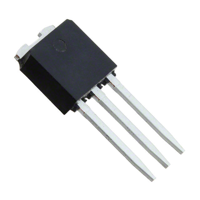
| 产品图片 |
|
| 产品型号 | STD2NK60Z-1 |
| rohs | 无铅 / 符合限制有害物质指令(RoHS)规范要求 |
| 产品系列 | SuperMESH™ |
| 不同Id时的Vgs(th)(最大值) | 4.5V @ 50µA |
| 不同Vds时的输入电容(Ciss) | 170pF @ 25V |
| 不同Vgs时的栅极电荷(Qg) | 10nC @ 10V |
| 不同 Id、Vgs时的 RdsOn(最大值) | 8 欧姆 @ 700mA,10V |
| 供应商器件封装 | I-Pak |
| 其它名称 | 497-12555-5 |
| 其它有关文件 | http://www.st.com/web/catalog/sense_power/FM100/CL824/SC1167/PF78366?referrer=70071840 |
| 功率-最大值 | 45W |
| 包装 | 管件 |
| 安装类型 | 通孔 |
| 封装/外壳 | TO-251-3 长引线,IPak,TO-251AB |
| 标准包装 | 75 |
| 漏源极电压(Vdss) | 600V |
| 电流-连续漏极(Id)(25°C时) | 1.4A (Tc) |


- 商务部:美国ITC正式对集成电路等产品启动337调查
- 曝三星4nm工艺存在良率问题 高通将骁龙8 Gen1或转产台积电
- 太阳诱电将投资9.5亿元在常州建新厂生产MLCC 预计2023年完工
- 英特尔发布欧洲新工厂建设计划 深化IDM 2.0 战略
- 台积电先进制程称霸业界 有大客户加持明年业绩稳了
- 达到5530亿美元!SIA预计今年全球半导体销售额将创下新高
- 英特尔拟将自动驾驶子公司Mobileye上市 估值或超500亿美元
- 三星加码芯片和SET,合并消费电子和移动部门,撤换高东真等 CEO
- 三星电子宣布重大人事变动 还合并消费电子和移动部门
- 海关总署:前11个月进口集成电路产品价值2.52万亿元 增长14.8%


PDF Datasheet 数据手册内容提取
STF2NK60Z - STQ2NK60ZR-AP STP2NK60Z - STD2NK60Z-1 Ω N-CHANNEL 600V - 7.2 - 1.4A TO-220/TO-220FP/TO-92/IPAK Zener-Protected SuperMESH™ MOSFET Table 1: General Features Figure 1: Package TYPE VDSS RDS(on) ID Pw STF2NK60Z 600 V < 8 Ω 1.4 A 20 STQ2NK60ZR-AP 600 V < 8 Ω 0.4 A 3 W STP2NK60Z 600 V < 8 Ω 1.4 A 45 W STD2NK60Z-1 600 V < 8 Ω 1.4 A 45 W 3 (cid:1) TYPICAL RDS(on) = 7.2 Ω TO-92 (Ammopack) 1 2 (cid:1) EXTREMELY HIGH dv/dt CAPABILITY TO-220 (cid:1) ESD IMPROVED CAPABILITY (cid:1) 100% AVALANCHE TESTED (cid:1) NEW HIGH VOLTAGE BENCHMARK (cid:1) GATE CHARGE MINIMIZED 3 2 1 3 2 DESCRIPTION 1 IPAK The SuperMESH™ series is obtained through an TO-220FP extreme optimization of ST’s well established strip-based PowerMESH™ layout. In addition to Figure 2: Internal Schematic Diagram pushing on-resistance significantly down, special care is taken to ensure a very good dv/dt capability for the most demanding applications. Such series complements ST full range of high voltage MOS- FETs including revolutionary MDmesh™ products. APPLICATIONS (cid:1) LOW POWER BATTERY CHARGERS (cid:1) SWITH MODE LOW POWER SUPPLIES(SMPS) (cid:1) LOW POWER, BALLAST, CFL (COMPACT FLUORESCENT LAMPS) Table 2: Order Codes Part Number Marking Package Packaging STQ2NK60ZR-AP Q2NK60ZR TO-92 AMMOPAK STP2NK60Z P2NK60Z TO-220 TUBE STD2NK60Z-1 D2NK60Z IPAK TUBE STF2NK60Z F2NK60Z TO-220FP TUBE Rev. 5 September 2005 1/16
STQ2NK60ZR-AP - STP2NK60Z - STF2NK60Z - STD2NK60Z-1 Table 3: Absolute Maximum ratings Symbol Parameter Value Unit TO-220 / TO-92 TO-220FP IPAK VDS Drain-source Voltage (VGS = 0) 600 V VDGR Drain-gate Voltage (RGS = 20 kΩ) 600 V VGS Gate- source Voltage ± 30 V ID Drain Current (continuous) at TC = 25°C 1.4 0.4 1.4 (*) A ID Drain Current (continuous) at TC = 100°C 0.77 0.25 0.77 (*) A IDM ((cid:1)) Drain Current (pulsed) 5.6 1.6 5.6 (*) A PTOT Total Dissipation at TC = 25°C 45 3 20 W Derating Factor 0.36 0.025 0.16 W/°C VESD(G-S) Gate source ESD (HBM-C= 100pF, R=1.5kΩ) 1500 V VISO Insulation Withstand Voltage (DC) 2500 V dv/dt (1) Peak Diode Recovery voltage slope 4.5 V/ns Tj Operating Junction Temperature -55 to 150 °C Tstg Storage Temperature (cid:1) ( ) Pulse width limited by safe operating area (1) ISD ≤ 1.4A, di/dt ≤ 200A/µs, VDD ≤ V(BR)DSS, Tj ≤ TJMAX. (*) Limited only by maximum temperature allowed Table 4: Thermal Data TO-220/IPAK TO-220FP TO-92 Unit Rthj-case Thermal Resistance Junction-case Max 2.77 6.25 -- °C/W Rthj-amb Thermal Resistance Junction-ambient Max 100 100 120 °C/W Rthj-lead Thermal Resistance Junction-lead Max -- -- 40 °C/W Tl Maximum Lead Temperature For Soldering 300 260 °C Purpose Table 5: Avalanche Characteristics Symbol Parameter Max Value Unit IAR Avalanche Current, Repetitive or Not-Repetitive 1.4 A (pulse width limited by Tj max) EAS Single Pulse Avalanche Energy 90 mJ (starting Tj = 25 °C, ID = IAR, VDD = 50 V) Table 6: Gate-Source Zener Diode Symbol Parameter Test Conditions Min. Typ. Max. Unit BVGSO Gate source Igs= ± 1 mA (Open Drain) 30 V Breakdown Voltage PROTECTION FEATURES OF GATE-TO-SOURCE ZENER DIODES The built-in back-to-back Zener diodes have specifically been designed to enhance not only the device’s ESD capability, but also to make them safely absorb possible voltage transients that may occasionally be applied from gate to source. In this respect the Zener voltage is appropriate to achieve an efficient and cost-effective intervention to protect the device’s integrity. These integrated Zener diodes thus avoid the usage of external components. 2/16
STQ2NK60ZR-AP - STP2NK60Z - STF2NK60Z - STD2NK60Z-1 ELECTRICAL CHARACTERISTICS (TCASE =25°C UNLESS OTHERWISE SPECIFIED) Table 7: On/Off Symbol Parameter Test Conditions Min. Typ. Max. Unit V(BR)DSS Drain-source ID = 1mA, VGS = 0 600 V Breakdown Voltage IDSS Zero Gate Voltage VDS = Max Rating 1 µA Drain Current (VGS = 0) VDS = Max Rating, TC = 125 °C 50 µA IGSS Gate-body Leakage VGS = ± 20V ±10 µA Current (VDS = 0) VGS(th) Gate Threshold Voltage VDS = VGS, ID = 50 µA 3 3.75 4.5 V RDS(on) Static Drain-source On VGS = 10V, ID = 0.7 A 7.2 8 Ω Resistance Table 8: Dynamic Symbol Parameter Test Conditions Min. Typ. Max. Unit gfs (1) Forward Transconductance VDS = 15 V, ID= 0.7 A 1 S Ciss Input Capacitance VDS = 25V, f = 1 MHz, VGS = 0 170 pF Coss Output Capacitance 27 pF Crss Reverse Transfer Capacitance 5 pF Coss eq. (3) Equivalent Output Capacitance VGS = 0V, VDS = 0V to 480V 30 pF td(on) Turn-on Delay Time VDD = 300 V, ID = 0.65 A, 8 ns tr Rise Time RG= 4.7 Ω, VGS = 10 V 30 ns td(off) Turn-off Delay Time (Resistive Load see, Figure 22 ns tr Fall Time 22) 55 ns Qg Total Gate Charge VDD = 480V, ID = 1.5 A, 7.7 10 nC Qgs Gate-Source Charge VGS = 10V 1.7 nC Qgd Gate-Drain Charge (see, Figure 24) 4 nC Table 9: Source Drain Diode Symbol Parameter Test Conditions Min. Typ. Max. Unit ISD Source-drain Current 1.5 A ISDM (2) Source-drain Current (pulsed) 6 A VSD (1) Forward On Voltage ISD = 1.5 A, VGS = 0 1.6 V trr Reverse Recovery Time ISD = 1.3 A, di/dt = 100 A/µs 250 ns Qrr Reverse Recovery Charge VDD = 25V, Tj = 25°C 550 µC IRRM Reverse Recovery Current (see test circuit, Figure 23) 4.4 A trr Reverse Recovery Time ISD = 1.3 A, di/dt = 100 A/µs 300 ns Qrr Reverse Recovery Charge VDD = 25V, Tj = 150°C 690 µC IRRM Reverse Recovery Current (see test circuit, Figure 23) 4.6 A (1) Pulsed: Pulse duration = 300 µs, duty cycle 1.5 %. (2) Pulse width limited by safe operating area. (3) Coss eq. is defined as a constant equivalent capacitance giving the same charging time as Coss when VDS increases from 0 to 80% VDSS 3/16
STQ2NK60ZR-AP - STP2NK60Z - STF2NK60Z - STD2NK60Z-1 Figure 3: .Safe Operating Area For TO-220 Figure 6: Thermal Impedance For TO-220 Figure 4: Safe Operating Area For IPAK Figure 7: Thermal Impedance For IPAK Figure 5: Safe Operating Area For TO-92 Figure 8: Thermal Impedance For TO-92 4/16
STQ2NK60ZR-AP - STP2NK60Z - STF2NK60Z - STD2NK60Z-1 Figure 9: Safe Operating Area For TO-220FP Figure 12: Thermal Impedance For TO-220FP Figure 10: Output Characteristics Figure 13: Transfer Characteristics Figure 11: Transconductance Figure 14: Gate Charge vs Gate-source Voltage 5/16
STQ2NK60ZR-AP - STP2NK60Z - STF2NK60Z - STD2NK60Z-1 Figure 15: Static Drain-source On Resistance Figure 18: Source-Drain Forward Characteris- tics Figure 16: Capacitance Variations Figure 19: Maximum Avalanche Energy vs Temperature Figure 17: Normalized Gate Thereshold Volt- Figure 20: Normalized On Resistance vs Tem- age vs Temperature perature 6/16
STQ2NK60ZR-AP - STP2NK60Z - STF2NK60Z - STD2NK60Z-1 Figure 21: Normalized BVDSS vs Temperature 7/16
STQ2NK60ZR-AP - STP2NK60Z - STF2NK60Z - STD2NK60Z-1 Figure 22: Switching Times Test Circuit For Figure 24: Gate Charge Test Circuit Resistive Load Figure 23: Test Circuit For Inductive Load Switching and Diode Recovery Times 8/16
STQ2NK60ZR-AP - STP2NK60Z - STF2NK60Z - STD2NK60Z-1 In order to meet environmental requirements, ST offers these devices in ECOPACK® packages. These packages have a Lead-free second level interconnect . The category of second level interconnect is marked on the package and on the inner box label, in compliance with JEDEC Standard JESD97. The maximum ratings related to soldering conditions are also marked on the inner box label. ECOPACK is an ST trademark. ECOPACK specifications are available at: www.st.com 9/16
STQ2NK60ZR-AP - STP2NK60Z - STF2NK60Z - STD2NK60Z-1 TO-220 MECHANICAL DATA mm. inch DIM. MIN. TYP MAX. MIN. TYP. MAX. A 4.40 4.60 0.173 0.181 b 0.61 0.88 0.024 0.034 b1 1.15 1.70 0.045 0.066 c 0.49 0.70 0.019 0.027 D 15.25 15.75 0.60 0.620 E 10 10.40 0.393 0.409 e 2.40 2.70 0.094 0.106 e1 4.95 5.15 0.194 0.202 F 1.23 1.32 0.048 0.052 H1 6.20 6.60 0.244 0.256 J1 2.40 2.72 0.094 0.107 L 13 14 0.511 0.551 L1 3.50 3.93 0.137 0.154 L20 16.40 0.645 L30 28.90 1.137 øP 3.75 3.85 0.147 0.151 Q 2.65 2.95 0.104 0.116 10/16
STQ2NK60ZR-AP - STP2NK60Z - STF2NK60Z - STD2NK60Z-1 TO-92 AMMOPACK mm. inch DIM. MIN. TYP MAX. MIN. TYP. MAX. A1 4.45 4.95 0.170 0.194 T 3.30 3.94 0.130 0.155 T1 1.6 0.06 T2 2.3 0.09 d 0.41 0.56 0.016 0.022 P0 12.5 12.7 12.9 0.49 0.5 0.51 P2 5.65 6.35 7.05 0.22 0.25 0.27 F1, F2 2.44 2.54 2.94 0.09 0.1 0.11 delta H -2 2 -0.08 0.08 W 17.5 18 19 0.69 0.71 0.74 W0 5.7 6 6.3 0.22 0.23 0.24 W1 8.5 9 9.25 0.33 0.35 0.36 W2 0.5 0.02 H 18.5 20.5 0.72 0.80 H0 15.5 16 16.5 0.61 0.63 0.65 H1 25 0.98 D0 3.8 4 4.2 0.15 0.157 0.16 t 0.9 0.035 L 11 0.43 l1 3 0.11 delta P -1 1 -0.04 0.04 11/16
STQ2NK60ZR-AP - STP2NK60Z - STF2NK60Z - STD2NK60Z-1 TO-251 (IPAK) MECHANICAL DATA mm inch DIM. MIN. TYP. MAX. MIN. TYP. MAX. A 2.2 2.4 0.086 0.094 A1 0.9 1.1 0.035 0.043 A3 0.7 1.3 0.027 0.051 B 0.64 0.9 0.025 0.031 B2 5.2 5.4 0.204 0.212 B3 0.85 0.033 B5 0.3 0.012 B6 0.95 0.037 C 0.45 0.6 0.017 0.023 C2 0.48 0.6 0.019 0.023 D 6 6.2 0.236 0.244 E 6.4 6.6 0.252 0.260 G 4.4 4.6 0.173 0.181 H 15.9 16.3 0.626 0.641 L 9 9.4 0.354 0.370 L1 0.8 1.2 0.031 0.047 L2 0.8 1 0.031 0.039 H C A C2 A3 1 A L2 D L B3 B6 B B5 3 E = B2 = 2 G = = = = 1 L1 0068771-E 12/16
STQ2NK60ZR-AP - STP2NK60Z - STF2NK60Z - STD2NK60Z-1 TO-92 MECHANICAL DATA mm. inch DIM. MIN. TYP MAX. MIN. TYP. MAX. A 4.32 4.95 0.170 0.194 b 0.36 0.51 0.014 0.020 D 4.45 4.95 0.175 0.194 E 3.30 3.94 0.130 0.155 e 2.41 2.67 0.094 0.105 e1 1.14 1.40 0.044 0.055 L 12.70 15.49 0.50 0.610 R 2.16 2.41 0.085 0.094 S1 0.92 1.52 0.036 0.060 W 0.41 0.56 0.016 0.022 V 5° 5° 13/16
STQ2NK60ZR-AP - STP2NK60Z - STF2NK60Z - STD2NK60Z-1 TO-220FP MECHANICAL DATA mm. inch DIM. MIN. TYP MAX. MIN. TYP. MAX. A 4.4 4.6 0.173 0.181 B 2.5 2.7 0.098 0.106 D 2.5 2.75 0.098 0.108 E 0.45 0.7 0.017 0.027 F 0.75 1 0.030 0.039 F1 1.15 1.7 0.045 0.067 F2 1.15 1.7 0.045 0.067 G 4.95 5.2 0.195 0.204 G1 2.4 2.7 0.094 0.106 H 10 10.4 0.393 0.409 L2 16 0.630 L3 28.6 30.6 1.126 1.204 L4 9.8 10.6 .0385 0.417 L5 2.9 3.6 0.114 0.141 L6 15.9 16.4 0.626 0.645 L7 9 9.3 0.354 0.366 Ø 3 3.2 0.118 0.126 E A D B L3 L6 L7 1 F F 1 G H G 2 F 1 2 3 L5 L2 L4 14/16
STQ2NK60ZR-AP - STP2NK60Z - STF2NK60Z - STD2NK60Z-1 Table 10: Revision History Date Revision Description of Changes 07-Jul-2004 3 The document change from “TARGET” to “COMPLETE” New stylesheet 11/Nov/2004 4 Added TO-220FP 05-Sep-2005 5 Inserted Ecopack indication 15/16
STQ2NK60ZR-AP - STP2NK60Z - STF2NK60Z - STD2NK60Z-1 Information furnished is believed to be accurate and reliable. However, STMicroelectronics assumes no responsibility for the consequences of use of such information nor for any infringement of patents or other rights of third parties which may result from its use. No license is granted by implication or otherwise under any patent or patent rights of STMicroelectronics. Specifications mentioned in this publication are subject to change without notice. This publication supersedes and replaces all information previously supplied. STMicroelectronics products are not authorized for use as critical components in life support devices or systems without express written approval of STMicroelectronics. The ST logo is a registered trademark of STMicroelectronics All other names are the property of their respective owners © 2005 STMicroelectronics - All Rights Reserved STMicroelectronics group of companies Australia - Belgium - Brazil - Canada - China - Czech Republic - Finland - France - Germany - Hong Kong - India - Israel - Italy - Japan - Malaysia - Malta - Morocco - Singapore - Spain - Sweden - Switzerland - United Kingdom - United States of America 16/16