ICGOO在线商城 > 分立半导体产品 > 晶体管 - FET,MOSFET - 单 > SI5432DC-T1-GE3
 Datasheet下载
- 型号: SI5432DC-T1-GE3
- 制造商: Vishay
- 库位|库存: xxxx|xxxx
- 要求:
| 数量阶梯 | 香港交货 | 国内含税 |
| +xxxx | $xxxx | ¥xxxx |
查看当月历史价格
查看今年历史价格
SI5432DC-T1-GE3产品简介:
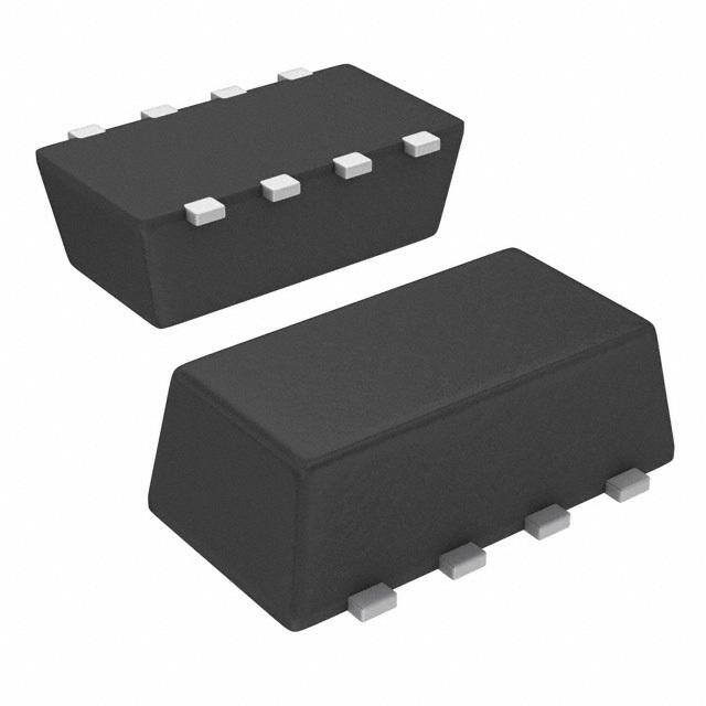
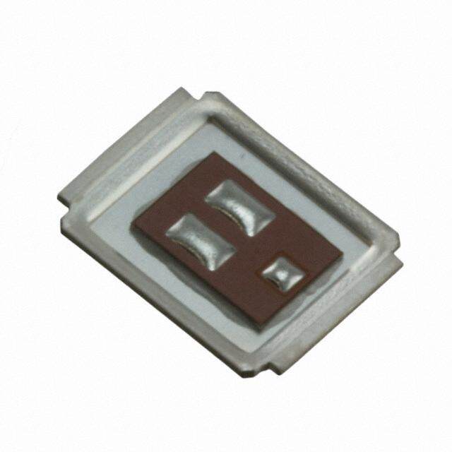
ICGOO电子元器件商城为您提供SI5432DC-T1-GE3由Vishay设计生产,在icgoo商城现货销售,并且可以通过原厂、代理商等渠道进行代购。 SI5432DC-T1-GE3价格参考。VishaySI5432DC-T1-GE3封装/规格:晶体管 - FET,MOSFET - 单, 表面贴装 N 沟道 20V 6A(Tc) 2.5W(Ta),6.3W(Tc) 1206-8 ChipFET™。您可以下载SI5432DC-T1-GE3参考资料、Datasheet数据手册功能说明书,资料中有SI5432DC-T1-GE3 详细功能的应用电路图电压和使用方法及教程。
Vishay Siliconix 的 SI5432DC-T1-GE3 是一款 P 沟道增强型 MOSFET,常用于需要高效功率控制和低导通电阻的应用中。该器件采用小型化封装(如 TDFN),适合空间受限的设计。

其主要应用场景包括:

1. 电源管理:用于 DC-DC 转换器、负载开关、电池供电设备中的高效电源控制。
2. 电机驱动:适用于小型电机或步进电机的驱动电路,提供快速开关和低损耗性能。
3. 负载开关与热插拔控制:在服务器、通信设备和工业控制系统中,用于控制电源通断,防止浪涌电流。
4. 汽车电子:用于车载电源系统、LED 照明控制、车载充电器等对可靠性和效率要求高的场景。
5. 消费类电子产品:如笔记本电脑、平板、智能家电等设备中的电源管理模块。

该 MOSFET 具有低导通电阻(Rds(on))、高可靠性及良好的热性能,适合高频开关应用,有助于提高系统效率并减少散热设计复杂度。
| 参数 | 数值 |
| 产品目录 | |
| ChannelMode | Enhancement |
| 描述 | MOSFET N-CH 20V 6A 1206-8MOSFET 20V 6.0A 6.3W 20mohm @ 4.5V |
| 产品分类 | FET - 单分离式半导体 |
| FET功能 | 逻辑电平门 |
| FET类型 | MOSFET N 通道,金属氧化物 |
| Id-ContinuousDrainCurrent | 6 A |
| Id-连续漏极电流 | 6 A |
| 品牌 | Vishay SiliconixVishay / Siliconix |
| 产品手册 | |
| 产品图片 |
|
| rohs | 符合RoHS无铅 / 符合限制有害物质指令(RoHS)规范要求 |
| 产品系列 | 晶体管,MOSFET,Vishay / Siliconix SI5432DC-T1-GE3TrenchFET® |
| 数据手册 | |
| 产品型号 | SI5432DC-T1-GE3SI5432DC-T1-GE3 |
| Pd-PowerDissipation | 2.5 W |
| Pd-功率耗散 | 2.5 W |
| RdsOn-Drain-SourceResistance | 20 mOhms |
| RdsOn-漏源导通电阻 | 20 mOhms |
| Vds-Drain-SourceBreakdownVoltage | 20 V |
| Vds-漏源极击穿电压 | 20 V |
| Vgs-Gate-SourceBreakdownVoltage | +/- 12 V |
| Vgs-栅源极击穿电压 | 12 V |
| 上升时间 | 10 ns |
| 下降时间 | 12 ns |
| 不同Id时的Vgs(th)(最大值) | 1.5V @ 250µA |
| 不同Vds时的输入电容(Ciss) | 1200pF @ 10V |
| 不同Vgs时的栅极电荷(Qg) | 33nC @ 10V |
| 不同 Id、Vgs时的 RdsOn(最大值) | 20 毫欧 @ 8.3A,4.5V |
| 产品目录页面 | |
| 产品种类 | MOSFET |
| 供应商器件封装 | 1206-8 ChipFET™ |
| 其它名称 | SI5432DC-T1-GE3TR |
| 典型关闭延迟时间 | 35 ns |
| 功率-最大值 | 6.3W |
| 包装 | 带卷 (TR) |
| 商标 | Vishay / Siliconix |
| 安装类型 | 表面贴装 |
| 安装风格 | SMD/SMT |
| 封装 | Reel |
| 封装/外壳 | 8-SMD,扁平引线 |
| 封装/箱体 | 1206-8 ChipFET |
| 工厂包装数量 | 3000 |
| 晶体管极性 | N-Channel |
| 最大工作温度 | + 150 C |
| 最小工作温度 | - 55 C |
| 标准包装 | 3,000 |
| 漏源极电压(Vdss) | 20V |
| 电流-连续漏极(Id)(25°C时) | 6A (Tc) |
| 通道模式 | Enhancement |
| 配置 | Single Hex Drain |
| 零件号别名 | SI5432DC-GE3 |


- 商务部:美国ITC正式对集成电路等产品启动337调查
- 曝三星4nm工艺存在良率问题 高通将骁龙8 Gen1或转产台积电
- 太阳诱电将投资9.5亿元在常州建新厂生产MLCC 预计2023年完工
- 英特尔发布欧洲新工厂建设计划 深化IDM 2.0 战略
- 台积电先进制程称霸业界 有大客户加持明年业绩稳了
- 达到5530亿美元!SIA预计今年全球半导体销售额将创下新高
- 英特尔拟将自动驾驶子公司Mobileye上市 估值或超500亿美元
- 三星加码芯片和SET,合并消费电子和移动部门,撤换高东真等 CEO
- 三星电子宣布重大人事变动 还合并消费电子和移动部门
- 海关总署:前11个月进口集成电路产品价值2.52万亿元 增长14.8%


PDF Datasheet 数据手册内容提取
New Product Si5432DC Vishay Siliconix N-Channel 20-V (D-S) MOSFET FEATURES PRODUCT SUMMARY • Halogen-free VDS (V) RDS(on) (Ω) ID (A)a Qg (Typ.) (cid:129) TrenchFET® Power MOSFET 0.020 at V = 4.5 V 6 RoHS GS 20 10 nC APPLICATIONS COMPLIANT 0.025 at V = 2.5 V 6 GS (cid:129) Load Switches for Portable Devices 1206-8ChipFETTM 1 D D D D D D D G G S S BottomView Ordering Information: Si5432DC-T1-GE3 (Lead (Pb)-free and Halogen-free) N-Channel MOSFET ABSOLUTE MAXIMUM RATINGS T = 25 °C, unless otherwise noted A Parameter Symbol Limit Unit Drain-Source Voltage VDS 20 V Gate-Source Voltage V ± 12 GS TC = 25 °C 6a Continuous Drain Current (T = 150 °C) TC = 70 °C I 6a J TA = 25 °C D 6a, b, c TA = 70 °C 6a, b, c A Pulsed Drain Current IDM 30 T = 25 °C 5.2 Continuous Source-Drain Diode Current TCA = 25 °C IS 2.1b, c TC = 25 °C 6.3 Maximum Power Dissipation TTCA == 2750 °°CC PD 2.54b, c W TA = 70 °C 1.6b, c Operating Junction and Storage Temperature Range TJ, Tstg - 55 to 150 °C Soldering Recommendations (Peak Temperature)e, f 260 THERMAL RESISTANCE RATINGS Parameter Symbol Typical Maximum Unit Maximum Junction-to-Ambienta, c, d t ≤ 5 s RthJA 40 50 °C/W Maximum Junction-to-Foot (Drain) Steady State RthJF 15 20 Notes: a.Package limited, T = 25 °C. C b.Surface Mounted on 1" x 1" FR4 board. c. t = 10 s. d.Maximum under Steady State conditions is 95 °C/W. e.See Reliability Manual for profile. The ChipFET is a leadless package. The end of the lead terminal is exposed copper (not plated) as a result of the singulation process in manufacturing. A solder fillet at the exposed copper tip cannot be guaranteed and is not required to ensure adequate bottom side solder interconnection. f. Rework Conditions: manual soldering with a soldering iron is not recommended for leadless components. Document Number: 68925 www.vishay.com S-82293-Rev. A, 22-Sep-08 1
New Product Si5432DC Vishay Siliconix SPECIFICATIONS T = 25 °C, unless otherwise noted J Parameter Symbol Test Conditions Min. Typ. Max. Unit Static Drain-Source Breakdown Voltage VDS VGS = 0 V, ID = 250 µA 20 V VDS Temperature Coefficient ΔVDS /TJ 25 I = 250 µA VGS(th) Temperature Coefficient ΔVGS(th)/TJ D - 4.0 mV/°C Gate-Source Threshold Voltage VGS(th) VDS = VGS , ID = 250 µA 0.6 1.5 V Gate-Source Leakage IGSS VDS = 0 V, VGS = ± 12 V ± 100 nA VDS = 20 V, VGS = 0 V 1 Zero Gate Voltage Drain Current IDSS VDS = 20 V, VGS = 0 V, TJ = 55 °C 10 µA On-State Drain Currenta ID(on) VDS ≥ 5 V, VGS = 4.5 V 30 A VGS = 4.5 V, ID = 8.3 A 0.016 0.020 Drain-Source On-State Resistancea RDS(on) Ω VGS = 2.5 V, ID = 4.5 A 0.020 0.025 Forward Transconductancea gfs VDS = 10 V, ID = 8.3 A 45 S Dynamicb Input Capacitance Ciss 1200 Output Capacitance Coss VDS = 10 V, VGS = 0 V, f = 1 MHz 220 pF Reverse Transfer Capacitance Crss 100 Total Gate Charge Qg VDS = 10 V, VGS = 10 V, ID = 8.3 A 22 33 10 15 nC Gate-Source Charge Qgs VDS = 10 V, VGS = 4.5 V, ID = 8.3 A 2.5 Gate-Drain Charge Qgd 1.7 Gate Resistance Rg f = 1 MHz 2.4 Ω Turn-on Delay Time td(on) 15 25 Rise Time tr VDD = 10 V, RL = 1.5 Ω 10 15 Turn-Off Delay Time td(off) ID ≅ 6.7 A, VGEN = 4.5 V, Rg = 1 Ω 35 55 Fall Time tf 12 20 ns Turn-on Delay Time td(on) 10 15 Rise Time tr VDD = 10 V, RL = 1.5 Ω 12 20 Turn-Off Delay Time td(off) ID ≅ 6.7 A, VGEN = 10 V, Rg = 1 Ω 25 40 Fall Time tf 10 15 Drain-Source Body Diode Characteristics Continuous Source-Drain Diode Current IS TC = 25 °C 5.2 A Pulse Diode Forward Current ISM 30 Body Diode Voltage VSD IS = 6.7 A, VGS = 0 V 0.8 1.2 V Body Diode Reverse Recovery Time trr 20 40 ns Body Diode Reverse Recovery Charge Qrr 10 20 nC I = 6.7 A, dI/dt = 100 A/µs, T = 25 °C F J Reverse Recovery Fall Time ta 10 ns Reverse Recovery Rise Time tb 10 Notes: a. Pulse test; pulse width ≤ 300 µs, duty cycle ≤ 2 % b. Guaranteed by design, not subject to production testing. Stresses beyond those listed under “Absolute Maximum Ratings” may cause permanent damage to the device. These are stress ratings only, and functional operation of the device at these or any other conditions beyond those indicated in the operational sections of the specifications is not implied. Exposure to absolute maximum rating conditions for extended periods may affect device reliability. www.vishay.com Document Number: 68925 2 S-82293-Rev. A, 22-Sep-08
New Product Si5432DC Vishay Siliconix TYPICAL CHARACTERISTICS 25°C, unless otherwise noted 30 10 VGS = 5 thru 2.5 V TC = - 55 °C 24 8 A) A) Drain Current ( 1128 VGS = 2 V Drain Current ( 46 TC = 125 °C - D - D I I 6 2 TC = 25 °C VGS = 1 V VGS = 1.5 V 0 0 0.0 0.5 1.0 1.5 2.0 2.5 3.0 0.0 0.5 1.0 1.5 2.0 VDS - Drain-to-Source Voltage (V) VGS- Gate-to-Source Voltage (V) Output Characteristics Transfer Characteristics 0.026 1500 0.024 Ciss 1200 Ω) 0.022 - On-Resistance (S(on) 0000....000011214608 VGS=4.5VVGS=2.5V C - Capacitance (pF) 690000 Coss D R 300 0.012 Crss 0.010 0 0 6 12 18 24 30 0 5 10 15 20 ID- Drain Current(A) VDS - Drain-to-Source Voltage (V) On-Resistance vs. Drain Current Capacitance 10 1.6 e (V) 8 ID = 8.3 A 1.4 ID = 8.3 A VGS = 4.5 V, 2.5 V ag VDS = 10 V e olt nc V a - Gate-to-Source 46 VDS = 16 V - On-ResistDS(on)(Normalized) 11..02 S R VG 2 0.8 0 0.6 0 5 10 15 20 25 - 50 - 25 0 25 50 75 100 125 150 Qg - Total Gate Charge (nC) TJ - Junction Temperature (°C) Gate Charge On-Resistance vs. Junction Temperature Document Number: 68925 www.vishay.com S-82293-Rev. A, 22-Sep-08 3
New Product Si5432DC Vishay Siliconix TYPICAL CHARACTERISTICS 25°C, unless otherwise noted 100 0.050 ID = 8.3 A 0.040 nt (A) Ωce () ce Curre 10 TJ = 150 °C TJ = 25 °C Resistan 0.030 our On- 0.020 TJ=125 °C - SS - n) I S(o TJ=25 °C D 0.010 R 1 0.000 0.0 0.2 0.4 0.6 0.8 1.0 1.2 0 1 2 3 4 5 VSD - Source-to-Drain Voltage (V) VGS- Gate-to-SourceVoltage(V) Source-Drain Diode Forward Voltage On-Resistance vs. Gate-to-Source Voltage 1.4 50 1.2 ID = 250 µA 40 (V)VGS(th) 01..80 ) W ( r e w o P 2300 0.6 10 0.4 0 - 50 - 25 0 25 50 75 100 125 150 0.001 0.01 0.1 1 10 100 600 TJ - Temperature (°C) Time (s) Threshold Voltage Single Pulse Power 100 LimitedbyRDS(on)* 100µs 10 nt (A) 1ms e urr 1 C 10ms n ai Dr 100ms - D 110ss I 0.1 DC BVDSS TA=25 °C Limited SinglePulse 0.01 0.1 1 10 100 VDS- Drain-to-SourceVoltage(V) *VGS>minimumVGSatwhichRDS(on)isspecified Safe Operating Area, Junction-to-Ambient www.vishay.com Document Number: 68925 4 S-82293-Rev. A, 22-Sep-08
New Product Si5432DC Vishay Siliconix TYPICAL CHARACTERISTICS 25°C, unless otherwise noted 18 8 15 6 A) 12 ent ( W) Curr 9 er( 4 Drain Package Limited Pow - 6 D I 2 3 0 0 0 25 50 75 100 125 150 25 50 75 100 125 150 TC- Case Temperature (°C) TC- Case Temperature (°C) Current Derating* Power Derating * The power dissipation P is based on T = 150 °C, using junction-to-case thermal resistance, and is more useful in settling the upper D J(max) dissipation limit for cases where additional heatsinking is used. It is used to determine the current rating, when this rating falls below the package limit. Document Number: 68925 www.vishay.com S-82293-Rev. A, 22-Sep-08 5
New Product Si5432DC Vishay Siliconix TYPICAL CHARACTERISTICS 25°C, unless otherwise noted 2 1 i t c e f f E d e z i l a m t n e i s n a r T e v e c n a d e p m I l a m r e h T 0.1 000D...u210t5y Cycle = 0.5 NPoD teMs : t 1 r o N 0.02 1. Duty Cyclet, 2 D = t 1 t 2 2. Per Unit Base = Rt hJA = 80 °C/W Single Pulse 3. T JM - TA = PDMZthJA(t) 4. Surface Mounted 0.01 10- 4 10- 3 10- 2 10- 1 1 10 100 600 Square Wave Pulse Duration (s) Normalized Thermal Transient Impedance, Junction-to-Ambient 2 1 v i e f E e z i l a m t c f d t n e i s n a r T e e c n a d e p m I l a m r e h T 0.1 000D.0..1u25 ty Cycle = 0.5 r o N 0.02 Single Pulse 0.01 10- 4 10- 3 10- 2 10- 1 1 10 Square Wave Pulse Duration (s) Normalized Thermal Transient Impedance, Junction-to-Foot Vishay Siliconix maintains worldwide manufacturing capability. Products may be manufactured at one of several qualified locations. Reliability data for Silicon Technology and Package Reliability represent a composite of all qualified locations. For related documents such as package/tape drawings, part marking, and reliability data, see http://www.vishay.com/ppg?68925. www.vishay.com Document Number: 68925 6 S-82293-Rev. A, 22-Sep-08
Package Information Vishay Siliconix 1206-8 ChipFET(cid:1) 4 L D 8 7 6 5 5 6 7 8 4 E1 E 4 3 2 1 1 2 3 4 x S e b c Backside View 2X 0.10/0.13 R A 1 C DETAIL X NOTES: 1. All dimensions are in millimeaters. 2. Mold gate burrs shall not exceed 0.13 mm per side. 3. Leadframe to molded body offset is horizontal and vertical shall not exceed 0.08 mm. 4. Dimensions exclusive of mold gate burrs. 5. No mold flash allowed on the top and bottom lead surface. MILLIMETERS INCHES Dim Min Nom Max Min Nom Max A 1.00 − 1.10 0.039 − 0.043 b 0.25 0.30 0.35 0.010 0.012 0.014 c 0.1 0.15 0.20 0.004 0.006 0.008 c1 0 − 0.038 0 − 0.0015 D 2.95 3.05 3.10 0.116 0.120 0.122 E 1.825 1.90 1.975 0.072 0.075 0.078 E1 1.55 1.65 1.70 0.061 0.065 0.067 e 0.65 BSC 0.0256 BSC L 0.28 − 0.42 0.011 − 0.017 S 0.55 BSC 0.022 BSC 5(cid:1)Nom 5(cid:1)Nom ECN: C-03528—Rev. F, 19-Jan-04 DWG: 5547 Document Number: 71151 www.vishay.com 15-Jan-04 1
AN811 Vishay Siliconix (cid:1) Single-Channel 1206-8 ChipFET Power MOSFET Recommended Pad Pattern and Thermal Performance INTRODUCTION New Vishay Siliconix ChipFETs in the leadless 1206-8 package feature the same outline as popular 1206-8 resistors 80 mil and capacitors but provide all the performance of true power semiconductor devices. The 1206-8 ChipFET has the same footprint as the body of the LITTLE FOOT(cid:1) TSOP-6, and can be thought of as a leadless TSOP-6 for purposes of visualizing board area, but its thermal performance bears comparison 68 mil with the much larger SO-8. This technical note discusses the single-channel ChipFET 1206-8 pin-out, package outline, pad patterns, evaluation board layout, and thermal performance. 28 mil PIN-OUT 26 mil FIGURE 2. Footprint With Copper Spreading Figure 1 shows the pin-out description and Pin 1 identification for the single-channel 1206-8 ChipFET device. The pin-out is similar to the TSOP-6 configuration, with two additional drain The pad pattern with copper spreading shown in Figure 2 pins to enhance power dissipation and thermal performance. improves the thermal area of the drain connections (pins The legs of the device are very short, again helping to reduce 1,2,3,6.7,8) while remaining within the confines of the basic the thermal path to the external heatsink/pcb and allowing a footprint. The drain copper area is 0.0054 sq. in. or larger die to be fitted in the device if necessary. 3.51 sq. mm). This will assist the power dissipation path away from the device (through the copper leadframe) and into the board and exterior chassis (if applicable) for the single device. Single 1206-8 ChipFET The addition of a further copper area and/or the addition of vias to other board layers will enhance the performance still further. 1 An example of this method is implemented on the D Vishay Siliconix Evaluation Board described in the next D D section (Figure 3). D D D G THE VISHAY SILICONIX EVALUATION S BOARD FOR THE SINGLE 1206-8 Bottom View The ChipFET 1206-08 evaluation board measures 0.6 in by FIGURE 1. 0.5 in. Its copper pad pattern consists of an increased pad area around the six drain leads on the top-side—approximately For package dimensions see the 1206-8 ChipFET package 0.0482 sq. in. 31.1 sq. mm—and vias added through to the outline drawing (http://www.vishay.com/doc?71151). underside of the board, again with a maximized copper pad area of approximately the board-size dimensions. The outer BASIC PAD PATTERNS package outline is for the 8-pin DIP, which will allow test sockets to be used to assist in testing. The basic pad layout with dimensions is shown in Application Note 826, Recommended Minimum Pad Patterns With Outline The thermal performance of the 1206-8 on this board has been Drawing Access for Vishay Siliconix MOSFETs, measured with the results following on the next page. The (http://www.vishay.com/doc?72286). This is sufficient for low testing included comparison with the minimum recommended power dissipation MOSFET applications, but power footprint on the evaluation board-size pcb and the industry semiconductor performance requires a greater copper pad standard one-inch square FR4 pcb with copper on both sides area, particularly for the drain leads. of the board. Document Number: 71126 www.vishay.com 12-Dec-03 1
AN811 Vishay Siliconix Front of Board Back of Board ChipFET(cid:1) vishay.com FIGURE 3. THERMAL PERFORMANCE The results show that a major reduction can be made in the thermal resistance by increasing the copper drain area. In this Junction-to-Foot Thermal Resistance example, a 45(cid:2)C/W reduction was achieved without having to (the Package Performance) increase the size of the board. If increasing board size is an option, a further 33(cid:2)C/W reduction was obtained by Thermal performance for the 1206-8 ChipFET measured as junction-to-foot thermal resistance is 15(cid:2)C/W typical, 20(cid:2)C/W maximizing the copper from the drain on the larger 1” square pcb. maximum for the single device. The “foot” is the drain lead of the device as it connects with the body. This is identical to the 160 SO-8 package R(cid:1)jf performance, a feat made possible by shortening the leads to the point where they become only a small part of the total footprint area. W) 120 Single EVB C/ Min. Footprint Junction-to-Ambient Thermal Resistance e ( c (dependent on pcb size) n a st 80 si T80h(cid:2)eC t/yWpi csatel aRd(cid:1)yj as tfaotre ,t hceo msipnagrlee-dc hwaitnhn e6l8 (cid:2)1C20/W6- 8fo Cr hthipeF SEOT- 8is. mal Re Maximum ratings are 95(cid:2)C/W for the 1206-8 versus 80(cid:2)C/W her 40 1” Square PCB T for the SO-8. Testing 0 To aid comparison further, Figure 4 illustrates ChipFET 1206-8 10-5 10-4 10-3 10-2 10-1 1 10 100 1000 thermal performance on two different board sizes and three Time (Secs) different pad patterns. The results display the thermal FIGURE 4. Single 1206−8 ChipFET performance out to steady state and produce a graphic SUMMARY account of how an increased copper pad area for the drain connections can enhance thermal performance. The measured steady state values of R(cid:1)ja for the single 1206-8 The thermal results for the single-channel 1206-8 ChipFET ChipFET are : package display similar power dissipation performance to the SO-8 with a footprint reduction of 80%. Careful design of the package has allowed for this performance to be achieved. The 1) Minimum recommended pad pattern (see 156(cid:2)C/W short leads allow the die size to be maximized and thermal Figure 2) on the evaluation board size of resistance to be reduced within the confines of the TSOP-6 0.5 in x 0.6 in. body size. 2) The evaluation board with the pad pattern 111(cid:2)C/W ASSOCIATED DOCUMENT described on Figure 3. 3) Industry standard 1” square pcb with 78(cid:2)C/W 1206-8 ChipFET Dual Thermal performance, AN812 maximum copper both sides. (http://www.vishay.com/doc?71127). www.vishay.com Document Number: 71126 2 12-Dec-03
Application Note 826 Vishay Siliconix RECOMMENDED MINIMUM PADS FOR 1206-8 ChipFET® 0.093 (2.357) 0 2) 6 4) 8 3 3 1 0 0 0 9 0. 2. 0. 0. ( ( 2 9) 2 5 0 5 0. 0. ( 0.026 0.016 0.010 (0.650) (0.406) (0.244) Recommended Minimum Pads Dimensions in Inches/(mm) Return to Index Return to Index E T O N N O I T A C I L P P A www.vishay.com Document Number: 72593 2 Revision: 21-Jan-08
Legal Disclaimer Notice www.vishay.com Vishay Disclaimer ALL PRODUCT, PRODUCT SPECIFICATIONS AND DATA ARE SUBJECT TO CHANGE WITHOUT NOTICE TO IMPROVE RELIABILITY, FUNCTION OR DESIGN OR OTHERWISE. Vishay Intertechnology, Inc., its affiliates, agents, and employees, and all persons acting on its or their behalf (collectively, “Vishay”), disclaim any and all liability for any errors, inaccuracies or incompleteness contained in any datasheet or in any other disclosure relating to any product. Vishay makes no warranty, representation or guarantee regarding the suitability of the products for any particular purpose or the continuing production of any product. To the maximum extent permitted by applicable law, Vishay disclaims (i) any and all liability arising out of the application or use of any product, (ii) any and all liability, including without limitation special, consequential or incidental damages, and (iii) any and all implied warranties, including warranties of fitness for particular purpose, non-infringement and merchantability. Statements regarding the suitability of products for certain types of applications are based on Vishay’s knowledge of typical requirements that are often placed on Vishay products in generic applications. Such statements are not binding statements about the suitability of products for a particular application. It is the customer’s responsibility to validate that a particular product with the properties described in the product specification is suitable for use in a particular application. Parameters provided in datasheets and / or specifications may vary in different applications and performance may vary over time. All operating parameters, including typical parameters, must be validated for each customer application by the customer’s technical experts. Product specifications do not expand or otherwise modify Vishay’s terms and conditions of purchase, including but not limited to the warranty expressed therein. Except as expressly indicated in writing, Vishay products are not designed for use in medical, life-saving, or life-sustaining applications or for any other application in which the failure of the Vishay product could result in personal injury or death. Customers using or selling Vishay products not expressly indicated for use in such applications do so at their own risk. Please contact authorized Vishay personnel to obtain written terms and conditions regarding products designed for such applications. No license, express or implied, by estoppel or otherwise, to any intellectual property rights is granted by this document or by any conduct of Vishay. Product names and markings noted herein may be trademarks of their respective owners. © 2017 VISHAY INTERTECHNOLOGY, INC. ALL RIGHTS RESERVED Revision: 08-Feb-17 1 Document Number: 91000