ICGOO在线商城 > 分立半导体产品 > 晶体管 - FET,MOSFET - 单 > IRFS7534-7PPBF
 Datasheet下载
- 型号: IRFS7534-7PPBF
- 制造商: International Rectifier
- 库位|库存: xxxx|xxxx
- 要求:
| 数量阶梯 | 香港交货 | 国内含税 |
| +xxxx | $xxxx | ¥xxxx |
查看当月历史价格
查看今年历史价格
IRFS7534-7PPBF产品简介:
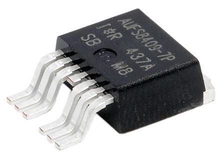
ICGOO电子元器件商城为您提供IRFS7534-7PPBF由International Rectifier设计生产,在icgoo商城现货销售,并且可以通过原厂、代理商等渠道进行代购。 IRFS7534-7PPBF价格参考。International RectifierIRFS7534-7PPBF封装/规格:晶体管 - FET,MOSFET - 单, 表面贴装 N 沟道 60V 240A(Tc) 290W(Tc) D2PAK(7-Lead)。您可以下载IRFS7534-7PPBF参考资料、Datasheet数据手册功能说明书,资料中有IRFS7534-7PPBF 详细功能的应用电路图电压和使用方法及教程。
Infineon Technologies(英飞凌科技)生产的型号为IRFS7534-7PPBF的晶体管属于FET(场效应晶体管)、MOSFET(金属氧化物半导体场效应晶体管)类别,且为单个器件。以下是该型号的主要应用场景:

 1. 电源管理
   - 开关电源(SMPS):IRFS7534-7PPBF适用于高效能的开关电源设计,能够处理高电流和高电压,提供稳定的电力输出。
   - DC-DC转换器:用于将直流电压从一个水平转换到另一个水平,广泛应用于汽车电子、工业设备和消费电子产品中。

 2. 电机驱动
   - 无刷直流电机(BLDC)驱动:该MOSFET可用于驱动无刷直流电机,具有低导通电阻(Rds(on)),可减少功率损耗并提高效率。
   - 步进电机控制:在需要精确控制的场景中,如打印机、扫描仪等,该器件可以提供可靠的性能。

 3. 工业自动化
   - 逆变器:用于太阳能逆变器或工业逆变器中,将直流电转换为交流电,支持可再生能源系统的运行。
   - 伺服系统:在工业机器人和自动化设备中,MOSFET可用于控制伺服电机的速度和位置。

 4. 汽车电子
   - 车载充电器(OBC):在电动汽车或混合动力汽车中,该MOSFET可用于车载充电器,实现高效的电池充电。
   - 电动助力转向(EPS):为车辆的电动助力转向系统提供稳定的动力支持。
   - 启动与停止系统:在现代汽车中,该器件可用于优化燃油效率的启动/停止系统。

 5. 消费电子产品
   - 笔记本电脑适配器:用于笔记本电脑和其他便携式设备的电源适配器中,确保高效的能量转换。
   - 游戏机电源模块:支持高性能游戏机的电源需求,提供稳定的供电。

 6. 通信设备
   - 基站电源:在通信基站中,该MOSFET可用于电源管理模块,确保信号传输的稳定性。
   - 网络设备:如路由器、交换机等,可用于电源管理和信号调节。

 特性优势
- 低导通电阻:减少能量损耗,提高系统效率。
- 高耐用性:能够在恶劣环境下工作,适合工业和汽车应用。
- 快速开关能力:支持高频操作,适用于现代电子设备的高效设计。

总之,IRFS7534-7PPBF凭借其优异的电气特性和可靠性,广泛应用于需要高效能、高可靠性的各种场景中。
| 参数 | 数值 |
| 产品目录 | |
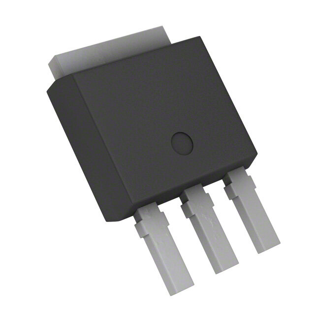
| 描述 | MOSFET N CH 60V 240A D2PAK |
| 产品分类 | FET - 单 |
| FET功能 | 标准 |
| FET类型 | MOSFET N 通道,金属氧化物 |
| 品牌 | International Rectifier |
| 数据手册 | |
| 产品图片 |
|
| 产品型号 | IRFS7534-7PPBF |
| rohs | 无铅 / 符合限制有害物质指令(RoHS)规范要求 |
| 产品系列 | HEXFET®, StrongIRFET™ |
| 不同Id时的Vgs(th)(最大值) | 3.7V @ 250µA |
| 不同Vds时的输入电容(Ciss) | 9990pF @ 25V |
| 不同Vgs时的栅极电荷(Qg) | 300nC @ 10V |
| 不同 Id、Vgs时的 RdsOn(最大值) | 1.95 毫欧 @ 100A, 10V |
| 供应商器件封装 | D2PAK(7-Lead) |
| 功率-最大值 | 290W |
| 包装 | 管件 |
| 安装类型 | 表面贴装 |
| 封装/外壳 | TO-263-7,D²Pak(6 引线+接片) |
| 标准包装 | 50 |
| 漏源极电压(Vdss) | 60V |
| 特色产品 | http://www.digikey.cn/product-highlights/zh/60-V-StrongIRFET-Power-MOSFETs/52378 |
| 电流-连续漏极(Id)(25°C时) | 240A (Tc) |
.jpg)


- 商务部:美国ITC正式对集成电路等产品启动337调查
- 曝三星4nm工艺存在良率问题 高通将骁龙8 Gen1或转产台积电
- 太阳诱电将投资9.5亿元在常州建新厂生产MLCC 预计2023年完工
- 英特尔发布欧洲新工厂建设计划 深化IDM 2.0 战略
- 台积电先进制程称霸业界 有大客户加持明年业绩稳了
- 达到5530亿美元!SIA预计今年全球半导体销售额将创下新高
- 英特尔拟将自动驾驶子公司Mobileye上市 估值或超500亿美元
- 三星加码芯片和SET,合并消费电子和移动部门,撤换高东真等 CEO
- 三星电子宣布重大人事变动 还合并消费电子和移动部门
- 海关总署:前11个月进口集成电路产品价值2.52万亿元 增长14.8%


PDF Datasheet 数据手册内容提取
StrongIRFET™ IRFS7534-7PPbF Application HEXFET® Power MOSFET Brushed motor drive applications BLDC motor drive applications V 60V D DSS Battery powered circuits R typ. 1.60m Half-bridge and full-bridge topologies DS(on) Synchronous rectifier applications max 1.95m G Resonant mode power supplies I 255A D (Silicon Limited) OR-ing and redundant power switches S DC/DC and AC/DC converters ID (Package Limited) 240A DC/AC inverters Benefits Improved gate, avalanche and dynamic dV/dt ruggedness Fully characterized capacitance and avalanche SOA Enhanced body diode dV/dt and dI/dt capability Lead-free, RoHS compliant G D S Gate Drain Source Base Part Number Package Type Standard Pack Complete Part Number Form Quantity Tube 50 IRFS7534-7PPbF IRFS7534-7PPbF D2Pak-7PIN Tape and Reel Left 800 IRFS7534TRL7PP ) 8 300 m ID = 100A Limited By Package ( e c 250 n a st 6 esi A) Rn (nt 200 O e cer Sou 4 TJ = 125°C rCnu rai 150 - no-t Dr,D 100 ia 2 I Dr , n) TJ = 25°C 50 o S( RD 0 0 4 6 8 10 12 14 16 18 20 25 50 75 100 125 150 175 VGS, Gate -to -Source Voltage (V) TC , Case Temperature (°C) Fig 1. Typical On-Resistance vs. Gate Voltage Fig 2. Maximum Drain Current vs. Case Temperature 1 www.irf.com © 2014 International Rectifier Submit Datasheet Feedback November 5, 2014
IRFS7534-7PPbF Absolute Maximum Rating Symbol Parameter Max. Units I @ T = 25°C Continuous Drain Current, V @ 10V (Silicon Limited) 255 D C GS I @ T = 100°C Continuous Drain Current, V @ 10V (Silicon Limited) 180 D C GS A I @ T = 25°C Continuous Drain Current, V @ 10V (Package Limited) 240 D C GS I Pulsed Drain Current 790 DM P @T = 25°C Maximum Power Dissipation 290 W D C Linear Derating Factor 2.0 W/°C V Gate-to-Source Voltage ± 20 V GS T Operating Junction and J -55 to + 175 TSTG Storage Temperature Range °C Soldering Temperature, for 10 seconds (1.6mm from case) 300 Avalanche Characteristics Symbol Parameter Max Units E Single Pulse Avalanche Energy 370 AS (Thermally limited) mJ E Single Pulse Avalanche Energy 773 AS (Thermally limited) I Avalanche Current A AR See Fig 15, 16, 23a, 23b E Repetitive Avalanche Energy mJ AR Thermal Resistance Symbol Parameter Typ. Max. Units R Junction-to-Case ––– 0.51 JC °C/W R Junction-to-Ambient ––– 40 JA Static @ T = 25°C (unless otherwise specified) J Symbol Parameter Min. Typ. Max. Units Conditions V Drain-to-Source Breakdown Voltage 60 ––– ––– V V = 0V, I = 250µA (BR)DSS GS D V /T Breakdown Voltage Temp. Coefficient ––– 46 ––– mV/°C Reference to 25°C, I = 1mA (BR)DSS J D R Static Drain-to-Source On-Resistance ––– 1.60 1.95 V = 10V, I = 100A DS(on) GS D m ––– 2.00 ––– V = 6.0V, I = 50A GS D V Gate Threshold Voltage 2.1 ––– 3.7 V V = V , I = 250µA GS(th) DS GS D I Drain-to-Source Leakage Current ––– ––– 1.0 V = 60V, V = 0V DSS DS GS µA ––– ––– 150 V = 60V,V = 0V,T =125°C DS GS J I Gate-to-Source Forward Leakage ––– ––– 100 V = 20V GSS GS nA Gate-to-Source Reverse Leakage ––– ––– -100 V = -20V GS R Gate Resistance ––– 1.9 ––– G Notes: Calculated continuous current based on maximum allowable junction temperature. Bond wire current limit is 240A. Note that current limitations arising from heating of the device leads may occur with some lead mounting arrangements. (Refer to AN-1140) Repetitive rating; pulse width limited by max. junction temperature. Limited by T , starting T = 25°C, L = 74µH, R = 50, I = 100A, V =10V. Jmax J G AS GS I 100A, di/dt 1240A/µs, V V , T 175°C. SD DD (BR)DSS J Pulse width 400µs; duty cycle 2%. C eff. (TR) is a fixed capacitance that gives the same charging time as C while V is rising from 0 to 80% V . oss oss DS DSS C eff. (ER) is a fixed capacitance that gives the same energy as C while V is rising from 0 to 80% V . oss oss DS DSS R is measured at T approximately 90°C. J Limited by T , starting T = 25°C, L = 1mH, R = 50, I = 39A, V =10V. Jmax J G AS GS When mounted on 1" square PCB (FR-4 or G-10 Material). For recommended footprint and soldering techniques refer to application note #AN-994.please refer to application note to AN-994: http://www.irf.com/technical-info/appnotes/an-994.pdf 2 www.irf.com © 2013 International Rectifier Submit Datasheet Feedback November 5, 2014
IRFS7534-7PPbF Dynamic Electrical Characteristics @ T = 25°C (unless otherwise specified) J Symbol Parameter Min. Typ. Max. Units Conditions gfs Forward Transconductance 190 ––– ––– S V = 10V, I =100A DS D Q Total Gate Charge ––– 200 300 I = 100A g D Q Gate-to-Source Charge ––– 50 ––– V = 30V gs nC DS Q Gate-to-Drain Charge ––– 59 ––– V = 10V gd GS Q Total Gate Charge Sync. (Qg - Qgd) ––– 141 ––– sync t Turn-On Delay Time ––– 140 ––– V = 30V d(on) DD t Rise Time ––– 120 ––– I = 100A r D ns t Turn-Off Delay Time ––– 195 ––– R = 2.7 d(off) G t Fall Time ––– 86 ––– V = 10V f GS C Input Capacitance ––– 9990 ––– V = 0V iss GS C Output Capacitance ––– 915 ––– V = 25V oss DS C Reverse Transfer Capacitance ––– 590 ––– pF ƒ = 1.0MHz rss C Effective Output Capacitance (Energy Related) ––– 900 ––– V = 0V, V = 0V to 48V oss eff.(ER) GS DS C Output Capacitance (Time Related) ––– 1150 ––– V = 0V, V = 0V to 48V oss eff.(TR) GS DS Diode Characteristics Symbol Parameter Min. Typ. Max. Units Conditions Continuous Source Current MOSFET symbol I ––– ––– 255 D S (Body Diode) showing the A Pulsed Source Current integral reverse G I ––– ––– 790 SM (Body Diode) p-n junction diode. S V Diode Forward Voltage ––– ––– 1.2 V T = 25°C,I = 100A,V = 0V SD J S GS dv/dt Peak Diode Recovery dv/dt ––– 9.4 ––– V/ns T = 175°C,I =100A,V = 60V J S DS ––– 45 ––– T = 25°C V = 51V t Reverse Recovery Time ns J DD rr ––– 48 ––– T = 125°C I = 100A, J F ––– 64 ––– T = 25°C di/dt = 100A/µs J Q Reverse Recovery Charge nC rr ––– 78 ––– T = 125°C J I Reverse Recovery Current ––– 2.4 ––– A T = 25°C RRM J 3 www.irf.com © 2013 International Rectifier Submit Datasheet Feedback November 5, 2014
IRFS7534-7PPbF 1000 1000 VGS VGS TOP 15V TOP 15V 10V 10V A) 100 87..00VV A) 87..00VV enr(t Cur 10 BOTTOM 6554....0505VVVV (t enurrC100 BOTTOM 6554....0505VVVV e e c c ur ru o o S S o- 1 -o 4.5V tn- n-t 10 ai ia rD 4.5V Dr , D 0.1 , D I 60µs PULSE WIDTH I 60µs PULSE WIDTH Tj = 25°C Tj = 175°C 0.01 1 0.1 1 10 100 1000 0.1 1 10 100 1000 VDS, Drain-to-Source Voltage (V) VDS, Drain-to-Source Voltage (V) Fig 3. Typical Output Characteristics Fig 4. Typical Output Characteristics 1000 2.5 e ID = 100A c an VGS = 10V A)(nt 100 sitRes 2.0 erCu rucer 10 TJ = 175°C Oen oucrS d)azeli1.5 Soo-tanr-iD, ID 1 V6D0SµT sJ= P=2U 52VL5S°CE WIDTH o--tDanri, Rn) So(DmorN ( 1.0 0.1 0.5 2.0 3.0 4.0 5.0 6.0 7.0 8.0 -60-40-20 0 20 40 60 80100120140160180 VGS, Gate-to-Source Voltage (V) TJ , Junction Temperature (°C) Fig 5. Typical Transfer Characteristics Fig 6. Normalized On-Resistance vs. Temperature 100000 14.0 VGS = 0V, f = 1 MHZ Ciss = Cgs + Cgd, Cds SHORTED ID= 100A 12.0 CCrossss == CCdgsd + Cgd V)(e VDS= 48V F)pe( anc 10000 Ciss agtVo lucer 108..00 VVDDSS== 3102VV itpac Coss oSo- 6.0 aCC, 1000 Crss -tGaet 4.0 , S G V 2.0 100 0.0 1 10 100 0 50 100 150 200 250 VDS, Drain-to-Source Voltage (V) QG, Total Gate Charge (nC) Fig 7. Typical Capacitance vs. Fig 8. Typical Gate Charge vs. Drain-to-Source Voltage Gate-to-Source Voltage 4 www.irf.com © 2013 International Rectifier Submit Datasheet Feedback November 5, 2014
IRFS7534-7PPbF 1000 100µsec 1msec )A A) n(t 100 TJ = 175°C (t n 100 Limited by e e package urr rru C C anri De 10 TJ = 25°C e oucrS 10 OIANRP TEEHARI AST ION srve on-t- LRIDMSIT(oEnD) BY eR, DS 1 Da ri, D 1 Tc = 25°C 10msec I I Tj = 175°C DC VGS = 0V Single Pulse 0.1 0.1 0.0 0.2 0.4 0.6 0.8 1.0 1.2 1.4 1.6 0.1 1 10 VSD, Source-to-Drain Voltage (V) VDS, Drain-toSource Voltage (V) Fig 9. Typical Source-Drain Diode Forward Voltage Fig 10. Maximum Safe Operating Area )V 78 1.6 ge( Id = 1.0mA a olt 76 V wn 1.2 o 74 d k a eBr 72 )µJ e oucrS 70 y( ngerE 0.8 o- n-t 68 ai 0.4 Dr , S 66 S D )R B 64 0.0 V( -60-40-20 0 20 40 60 80100120140160180 -10 0 10 20 30 40 50 60 TJ , Temperature ( °C ) VDS, Drain-to-Source Voltage (V) Fig 11. Drain-to-Source Breakdown Voltage Fig 12. Typical C Stored Energy oss ) 4.0 m e( Vgs = 5.5V c an 3.5 Vgs = 6.0V ts Vgs = 7.0V esi Vgs = 8.0V R Vgs = 10V On 3.0 e c ur o S 2.5 o- n-t ai rD 2.0 ), n o (S D R 1.5 0 20 40 60 80 100 120 140 160 180 200 ID, Drain Current (A) Fig 13. Typical On-Resistance vs. Drain Current 5 www.irf.com © 2013 International Rectifier Submit Datasheet Feedback November 5, 2014
IRFS7534-7PPbF 1 W D = 0.50 C/ ° )C 0.1 00..2100 J h t 0.05 Z ( e 0.01 0.02 s n 0.01 o p s e R al m0.001 erh S( TINHGELREM PAULL RSEESPONSE ) Notes: T 1. Duty Factor D = t1/t2 2. Peak Tj = P dm x Zthjc + Tc 0.0001 1E-006 1E-005 0.0001 0.001 0.01 0.1 1 t1 , Rectangular Pulse Duration (sec) Fig 14. Maximum Effective Transient Thermal Impedance, Junction-to-Case 1000 Allowed avalanche Current vs avalanche pulsewidth, tav, assuming Tj = 150°C and Tstart =25°C (Single Pulse) A) ( tn 100 e rru C e h c n a al 10 v A Allowed avalanche Current vs avalanche pulsewidth, tav, assuming j = 25°C and Tstart = 150°C. 1 1.0E-06 1.0E-05 1.0E-04 1.0E-03 1.0E-02 tav (sec) Fig 15. Avalanche Current vs. Pulse width 400 TOP Single Pulse Notes on Repetitive Avalanche Curves , Figures 15, 16: (For further info, see AN-1005 at www.irf.com) BOTTOM 1.0% Duty Cycle 1.Avalanche failures assumption: J) ID = 100A Purely a thermal phenomenon and failure occurs at a m 300 y( temperature far in excess of Tjmax. This is validated for every g part type. nerE 2. Safe operation in Avalanche is allowed as long asTjmax is not e exceeded. h 200 3. Equation below based on circuit and waveforms shown in Figures c an 23a, 23b. alv 4. PD (ave) = Average power dissipation per single avalanche pulse. A, R 100 5 . BV = R aintecdre barseea kdduoriwngn avvoaltlaagnec h(1e.)3. factor accounts for voltage A E 6. Iav = Allowable avalanche current. 7. T = Allowable rise in junction temperature, not to exceed T jmax (assumed as 25°C in Figure 15, 16). 0 tav = Average time in avalanche. D = Duty cycle in avalanche = tav ·f 25 50 75 100 125 150 175 Z (D, t ) = Transient thermal resistance, see Figures 13) thJC av Starting TJ , Junction Temperature (°C) PD (ave) = 1/2 ( 1.3·BV·Iav) = T/ ZthJC I = 2T/ [1.3·BV·Z ] av th E = P t Fig 16. Maximum Avalanche Energy vs. Temperature AS (AR) D (ave)·av 6 www.irf.com © 2013 International Rectifier Submit Datasheet Feedback November 5, 2014
IRFS7534-7PPbF 4.0 20 IF = 60A V) 3.5 VR = 51V e( ag 15 TJ = 25°C oltV 3.0 TJ = 125°C d olesh 2.5 ID = 250µA )A( M 10 reht ta 2.0 IIDD == 11..00AmA IRR G , h) 1.5 5 S(t G 1.0 V 0.5 0 -75 -50 -25 0 25 50 75 100 125 150 175 0 200 400 600 800 1000 TJ , Temperature ( °C ) diF /dt (A/µs) Fig 17. Threshold Voltage vs. Temperature Fig 18. Typical Recovery Current vs. dif/dt 20 400 IF = 100A IF = 60A VR = 51V VR = 51V 15 TJ = 25°C 300 TJ = 25°C TJ = 125°C TJ = 125°C )A C) ( MR 10 n( R 200 R R I Q 5 100 0 0 0 200 400 600 800 1000 0 200 400 600 800 1000 diF /dt (A/µs) diF /dt (A/µs) Fig 19. Typical Recovery Current vs. dif/dt Fig 20. Typical Stored Charge vs. dif/dt 400 IF = 100A VR = 51V 300 TJ = 25°C TJ = 125°C C) n ( R 200 R Q 100 0 0 200 400 600 800 1000 diF /dt (A/µs) Fig 21. Typical Stored Charge vs. dif/dt 7 www.irf.com © 2013 International Rectifier Submit Datasheet Feedback November 5, 2014
IRFS7534-7PPbF Fig 22. Peak Diode Recovery dv/dt Test Circuit for N-Channel HEXFET® Power MOSFETs V(BR)DSS tp 15V VDS L DRIVER RG D.U.T + - VDD IAS A 20V tp 0.01 IAS Fig 23a. Unclamped Inductive Test Circuit Fig 23b. Unclamped Inductive Waveforms Fig 24a. Switching Time Test Circuit Fig 24b. Switching Time Waveforms Id Vds Vgs VDD Vgs(th) Qgs1 Qgs2 Qgd Qgodr Fig 25a. Gate Charge Test Circuit Fig 25b. Gate Charge Waveform 8 www.irf.com © 2013 International Rectifier Submit Datasheet Feedback November 5, 2014
IRFS7534-7PPbF D2Pak-7Pin Package Outline (Dimensions are shown in millimeters (inches)) Note: For the most current drawing please refer to IR website at http://www.irf.com/package/ 9 www.irf.com © 2013 International Rectifier Submit Datasheet Feedback November 5, 2014
IRFS7534-7PPbF D2Pak-7Pin Part Marking Information D2Pak-7Pin Tape and Reel Note: For the most current drawing please refer to IR website at http://www.irf.com/package/ 10 www.irf.com © 2013 International Rectifier Submit Datasheet Feedback November 5, 2014
IRFS7534-7PPbF Qualification Information† Industrial Qualification Level (per JEDEC JESD47F) †† Moisture Sensitivity Level D2Pak-7Pin MSL1 RoHS Compliant Yes † Qualification standards can be found at International Rectifier’s web site: http://www.irf.com/product-info/reliability/ †† Applicable version of JEDEC standard at the time of product release. Revision History Date Comments Updated E = 773mJ on page 2 11/5/2014 AS(L =1mH) Updated note 9 “Limited by T , starting T = 25°C, L = 1mH, R = 50, I = 39A, V =10V” on page 2 Jmax J G AS GS IR WORLD HEADQUARTERS: 101 N. Sepulveda Blvd., El Segundo, California 90245, USA To contact International Rectifier, please visit http://www.irf.com/whoto-call/ 11 www.irf.com © 2013 International Rectifier Submit Datasheet Feedback November 5, 2014
Mouser Electronics Authorized Distributor Click to View Pricing, Inventory, Delivery & Lifecycle Information: I nfineon: IRFS7534TRL7PP IRFS7534-7PPBF