ICGOO在线商城 > 分立半导体产品 > 晶体管 - FET,MOSFET - 单 > IRFD9010PBF
 Datasheet下载
- 型号: IRFD9010PBF
- 制造商: Vishay
- 库位|库存: xxxx|xxxx
- 要求:
| 数量阶梯 | 香港交货 | 国内含税 |
| +xxxx | $xxxx | ¥xxxx |
查看当月历史价格
查看今年历史价格
IRFD9010PBF产品简介:
ICGOO电子元器件商城为您提供IRFD9010PBF由Vishay设计生产,在icgoo商城现货销售,并且可以通过原厂、代理商等渠道进行代购。 IRFD9010PBF价格参考。VishayIRFD9010PBF封装/规格:晶体管 - FET,MOSFET - 单, 通孔 P 沟道 50V 1.1A(Tc) 1W(Tc) 4-DIP,Hexdip,HVMDIP。您可以下载IRFD9010PBF参考资料、Datasheet数据手册功能说明书,资料中有IRFD9010PBF 详细功能的应用电路图电压和使用方法及教程。
IRFD9010PBF是由Vishay Siliconix生产的一款N沟道增强型MOSFET(金属氧化物半导体场效应晶体管)。其主要应用场景包括:

1. 开关电源(SMPS):
   IRFD9010PBF适用于开关电源中的功率转换电路,例如DC-DC转换器、降压或升压转换器等。其低导通电阻(Rds(on))和高击穿电压(Vds)使其能够高效地处理高电压和大电流。

2. 电机驱动:
   该器件可用于小型直流电机或步进电机的驱动电路中,作为开关元件控制电机的启动、停止和速度调节。其快速开关特性和低功耗特性有助于提高系统效率。

3. 负载开关:
   在需要动态控制负载的应用中(如电池供电设备),IRFD9010PBF可以用作负载开关,实现对不同负载的精确控制,同时减少能量损耗。

4. 逆变器电路:
   在太阳能逆变器或其他类型的逆变器中,这款MOSFET可以用于将直流电转换为交流电的高频开关操作。

5. 保护电路:
   它也可以用作过流保护或短路保护的开关元件,通过快速响应切断异常电流路径,从而保护整个电路系统。

6. 音频功率放大器:
   在某些音频应用中,IRFD9010PBF可用作输出级的开关元件,提供高效的信号放大功能。

7. 汽车电子:
   由于其耐高压能力,该器件适合用于汽车电子中的各种控制模块,如车窗升降器、雨刷控制器以及照明系统等。

总之,IRFD9010PBF凭借其出色的电气性能和可靠性,广泛应用于工业控制、消费电子产品、通信设备以及汽车领域中的各种功率管理和信号处理场景。
| 参数 | 数值 |
| 产品目录 | |
| ChannelMode | Enhancement |
| 描述 | MOSFET P-CH 50V 1.1A 4-DIPMOSFET P-Chan 50V 1.1 Amp |
| 产品分类 | FET - 单分离式半导体 |
| FET功能 | 标准 |
| FET类型 | MOSFET P 通道,金属氧化物 |
| Id-ContinuousDrainCurrent | 1.1 A |
| Id-连续漏极电流 | 1.1 A |
| 品牌 | Vishay / Siliconix |
| 产品手册 | |
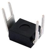
| 产品图片 |
|
| rohs | RoHS 合规性豁免无铅 / 符合限制有害物质指令(RoHS)规范要求 |
| 产品系列 | 晶体管,MOSFET,Vishay / Siliconix IRFD9010PBF- |
| 数据手册 | |
| 产品型号 | IRFD9010PBF |
| Pd-PowerDissipation | 1 W |
| Pd-功率耗散 | 1 W |
| RdsOn-Drain-SourceResistance | 350 mOhms |
| RdsOn-漏源导通电阻 | 350 mOhms |
| Vds-Drain-SourceBreakdownVoltage | 50 V |
| Vds-漏源极击穿电压 | - 50 V |
| Vgs-Gate-SourceBreakdownVoltage | 20 V |
| Vgs-栅源极击穿电压 | 20 V |
| 上升时间 | 47 ns |
| 下降时间 | 39 ns |
| 不同Id时的Vgs(th)(最大值) | 4V @ 250µA |
| 不同Vds时的输入电容(Ciss) | 240pF @ 25V |
| 不同Vgs时的栅极电荷(Qg) | 11nC @ 10V |
| 不同 Id、Vgs时的 RdsOn(最大值) | 500 毫欧 @ 580mA,10V |
| 产品目录绘图 |
|
| 产品目录页面 | |
| 产品种类 | MOSFET |
| 供应商器件封装 | 4-DIP,Hexdip,HVMDIP |
| 其它名称 | *IRFD9010PBF |
| 典型关闭延迟时间 | 13 ns |
| 功率-最大值 | 1W |
| 包装 | 管件 |
| 商标 | Vishay / Siliconix |
| 安装类型 | 通孔 |
| 安装风格 | Through Hole |
| 封装 | Tube |
| 封装/外壳 | 4-DIP(0.300",7.62mm) |
| 封装/箱体 | DIP-4 |
| 工厂包装数量 | 2500 |
| 晶体管极性 | P-Channel |
| 最大工作温度 | + 125 C |
| 最小工作温度 | - 55 C |
| 标准包装 | 2,500 |
| 正向跨导-最小值 | 2.5 S |
| 漏源极电压(Vdss) | 50V |
| 电流-连续漏极(Id)(25°C时) | 1.1A (Tc) |
| 通道模式 | Enhancement |
| 配置 | Single |


PDF Datasheet 数据手册内容提取
IRFD9010, SiHFD9010 Vishay Siliconix Power MOSFET FEATURES PRODUCT SUMMARY • For Automatic Insertion V (V) - 50 • Compact, End Stackable DS • Fast Switching RDS(on) (Ω) VGS = - 10 V 0.50 • Low Drive Current Q (Max.) (nC) 11 g • Easy Paralleled Qgs (nC) 3.8 • Excellent Temperature Stability Qgd (nC) 4.1 • P-Channel Versatility Configuration Single • Compliant to RoHS Directive 2002/95/EC DESCRIPTION The HVMDIP technology is the key to Vishay’s advanced line of power MOSFET transistors. The efficient geometry S and unique processing of the HVMDIP design achieves very low on-state resistance combined with high HVMDIP transconductance and extreme device ruggedness. The p-channel HVMDIPs are designed for application which G require the convenience of reverse polarity operation. They retain all of the features of the more common n-channel HVMDIPs such as voltage control, very fast switching, ease S of paralleling, and excellent temperature stability. G P-channels HVMDIPs are intended for use in power stages D D where complementary symmetry with n-channel devices offers circuit simplification. They are also very useful in drive P-Channel MOSFET stages because of the circuit versatility offered by the reverse polarity connection. Applications include motor control, audio amplifiers, switched mode converters, control circuits and pulse amplifiers. ORDERING INFORMATION Package HVMDIP IRFD9010PbF Lead (Pb)-free SiHFD9010-E3 IRFD9010 SnPb SiHFD9010 ABSOLUTE MAXIMUM RATINGS (T = 25 °C, unless otherwise noted) C PARAMETER SYMBOL LIMIT UNIT Drain-Source Voltage V - 50 DS V Gate-Source Voltage V ± 20 GS T = 25 °C - 1.1 C Continuous Drain Current V at - 10 V I GS D T = 100 °C - 0.68 A C Pulsed Drain Currenta I - 8.8 DM Linear Derating Factor 0.01 W/°C Inductive Current, Clamped L = 100 µH see fig. 14 I - 8.8 LM A Inductive Current, Unclamped (Avalanche Current) see fig. 15 I - 1.5 L Maximum Power Dissipation T = 25 °C P 1 W C D Operating Junction and Storage Temperature Range T , T - 55 to + 150 J stg °C Soldering Recommendations (Peak Temperature) for 10 s 300d Notes a. Repetitive rating; pulse width limited by maximum junction temperature (see fig. 11). b. VDD = - 25 V, starting TJ = 25 °C, L = 52 mH, Rg = 25 Ω, IAS = - 2.0 A (see fig. 12). c. ISD ≤ - 4.0 A, dI/dt ≤ 75 A/μs, VDD ≤ VDS, TJ ≤ 175 °C. d. 1.6 mm from case. * Pb containing terminations are not RoHS compliant, exemptions may apply Document Number: 91405 www.vishay.com S10-0998-Rev. A, 26-Apr-10 1
IRFD9010, SiHFD9010 Vishay Siliconix THERMAL RESISTANCE RATINGS PARAMETER SYMBOL TYP. MAX. UNIT Maximum Junction-to-Ambient R - 120 °C/W thJA SPECIFICATIONS (T = 25 °C, unless otherwise noted) J PARAMETER SYMBOL TEST CONDITIONS MIN. TYP. MAX. UNIT Static Drain-Source Breakdown Voltage V V = 0 V, I = - 250 μA - 50 - - V DS GS D VDS Temperature Coefficient ΔVDS/TJ Reference to 25 °C, ID = - 1 mA - - 0.091 - V/°C Gate-Source Threshold Voltage V V = V , I = - 250 μA - 2.0 - - 4.0 V GS(th) DS GS D Gate-Source Leakage I V = ± 20 V - - ± 500 nA GSS GS V = - 50 V, V = 0 V - - - 250 DS GS Zero Gate Voltage Drain Current I μA DSS V = - 40 V, V = 0 V, T = 125 °C - - - 1000 DS GS J On-State Drain Current I V = 10 V V > I x R max. - 1.1 - - A D(on) GS DS D(on) DS(on) Drain-Source On-State Resistance RDS(on) VGS = - 10 V ID = - 0.58 Ab - 0.35 0.50 Ω Forward Transconductance g V = - 20 V, I = - 2.4 A 1.7 2.5 - S fs DS D Dynamic Input Capacitance C - 240 - iss V = 0 V, GS Output Capacitance C V = - 25 V, - 160 - pF oss DS f = 1.0 MHz, see fig. 5 Reverse Transfer Capacitance C - 30 - rss Total Gate Charge Q - 7.2 11 g I = - 4.7 A, V = 0.8 V Gate-Source Charge Q V = - 10 V D DS - 2.5 3.8 nC gs GS see fig. 6 and 13b Gate-Drain Charge Q - 2.7 4.1 gd Turn-On Delay Time t - 6.1 9.2 d(on) Rise Time tr VDD = - 25 V, ID = - 4.7 A - 47 71 Rg = 24 Ω, RD = 5.6 Ω, ns Turn-Off Delay Time td(off) see fig. 10b - 13 20 Fall Time t - 39 59 f Internal Drain Inductance L Between lead, D - 4.0 - D 6 mm (0.25") from nH package and center of G Internal Source Inductance L - 6.0 - S die contact S Drain-Source Body Diode Characteristics MOSFET symbol Continuous Source-Drain Diode Current IS D - - - 1.1 A showing the integral reverse G Pulsed Diode Forward Currenta I - - - 8.8 SM p - n junction diode S Body Diode Voltage V T = 25 °C, I = - 0.7 A, V = 0 Vb - - - 5.5 V SD J S GS Body Diode Reverse Recovery Time t 33 75 160 ns rr T = 25 °C, I = - 4.7 A, dI/dt = 100 A/μsb J F Body Diode Reverse Recovery Charge Q 0.090 0.22 0.52 μC rr Forward Turn-On Time t Intrinsic turn-on time is negligible (turn-on is dominated by L and L ) on S D Notes a. Repetitive rating; pulse width limited by maximum junction temperature (see fig. 11). b. Pulse width ≤ 300 μs; duty cycle ≤ 2 %. www.vishay.com Document Number: 91405 2 S10-0998-Rev. A, 26-Apr-10
IRFD9010, SiHFD9010 Vishay Siliconix TYPICAL CHARACTERISTICS (25 °C, unless otherwise noted) 10 e 3.0 - 10 V 80 μs Pulse Width - 8 V stanc ID = - 4.7 V 8 si 2.4 A) Re Current ( 6 - 7 V urce on alized) 1.8 n Som - I, DraiD 42 VGS = -- 65 VV Drain-to-(Nor 10..26 - 4 V , S(on) VGS = - 10 V D 0 R 0 0 5 10 15 20 25 - 60- 40- 20 0 20 40 60 80 100120140160 - V , Drain-to-Source Voltage (V) T , Junction Temperature (°C) GS J Fig. 1 - Typical Output Characteristics Fig. 4 - Normalized On-Resistance vs. Temperature 10 500 80 μs Pulse Width V = 0 V, f = 1 MHz GS - 10 V C = C + C , C Shorted iss gs gd ds C = C 8 400 rss gd A) - 8 V Coss = Cds + Cgd nt ( pF) urre 6 - 7 V ce ( 300 Ciss C n Drain 4 V = - 6 V pacita 200 , D GS Ca Coss - I 2 100 - 5 V C rss - 4 V 0 0 0 1 2 3 4 5 1 10 100 - V , Drain-to-Source Voltage (V) - V , Drain-to-Source Voltage (V) GS GS Fig. 2 - Typical Output Characteristics Fig. 5 - Typical Capacitance vs. Drain-to-Source Voltage 10 20 8V0D Sμ =s P2 uxl sVeG WSidth e (V) ID = - 4.7 A g 16 urrent (A) 1 urce Volta 12 VDS = - 40 V C 0.1 T = 150 °C o n J S ai o- 8 Dr -t , D TJ = 25 °C ate - I 0.01 , GS 4 VG For Test Circuit - See Figure 13 0.001 0 0 3 4 6 8 10 0 3 6 9 12 15 - V , Drain-to-Source Voltage (V) Q , Total Gate Charge (nC) GS g Fig. 3 - Typical Transfer Characteristics Fig. 6 - Typical Gate Charge vs. Gate-to-Source Voltage Document Number: 91405 www.vishay.com S10-0998-Rev. A, 26-Apr-10 3
IRFD9010, SiHFD9010 Vishay Siliconix 100 2.0 A) ent ( A) 1.6 everse Drain Curr 101 TTJ J= = 1 2550 °°CC , Drain Current (D 10..28 , RD - I 0.4 S - I 0.1 0 0 1 2 3 4 5 25 50 75 100 125 150 - VSD, Source-to-Drain Voltage (V) TC, Case Temperature (°C) Fig. 7 - Typical Source-Drain Diode Forward Voltage Fig. 9 - Maximum Drain Current vs. Case Temperature 100 Operation in this Area Limited RD by RDS(on) VDS A) 10 10 μs VGS ent ( 100 μs Rg D.U.T. - urr 1 ms +VDD C 1 n - 10 V ai 10 ms Dr Pulse width ≤ 1 µs , D 100 ms Duty factor ≤ 0.1 % - I 0.1 T = 25 °C 1 s C Fig. 10a - Switching Time Test Circuit T = 150 °C J DC Single Pulse 0.01 1 10 100 - VDS, Drain-to-Source Voltage (V) td(on) tr td(off) tf V GS Fig. 8 - Maximum Safe Operating Area 10 % 90 % V DS Fig. 10b - Switching Time Waveforms www.vishay.com Document Number: 91405 4 S10-0998-Rev. A, 26-Apr-10
IRFD9010, SiHFD9010 Vishay Siliconix 1000 )C J Dth 100 0.5 Z e ( 0.2 s n 0.1 o sp 10 0.05 PDM e R 0.02 al t1 m t er 1 0.01 Notes: 2 h T Single Pulse 1. Duty Factor, D = t1/t2 2. Peak T = P x T + T (Thermal Response) J DM thJC C 0.1 0.00001 0.0001 0.001 0.01 0.1 1 10 100 t , Rectangular Pulse Duration (s) 1 Fig. 11 - Maximum Effective Transient Thermal Impedance, Junction-to-Case L VDS QG Vary tp to obtain - 10 V required IAS Rg D.U.T - QGS QGD +VDD I AS V - 10 V G tp 0.01 W Charge Fig. 12a - Unclamped Inductive Test Circuit Fig. 13a - Basic Gate Charge Waveform Current regulator Same type as D.U.T. I AS 50 kΩ 12 V 0.2 µF 0.3 µF V DS - V D.U.T. + DS V DD tp VGS - 3 mA V DS I I G D Current sampling resistors Fig. 12b - Unclamped Inductive Waveforms Fig. 13b - Gate Charge Test Circuit Document Number: 91405 www.vishay.com S10-0998-Rev. A, 26-Apr-10 5
IRFD9010, SiHFD9010 Vishay Siliconix Peak Diode Recovery dV/dt Test Circuit D.U.T. + Circuit layout considerations • Low stray inductance • Ground plane • Low leakage inductance current transformer - + - + - Rg • dV/dt controlled by RG + • ISD controlled by duty factor "D" - VDD • D.U.T. - device under test Compliment N-Channel of D.U.T. for driver Driver gate drive P.W. Period D = P.W. Period V = - 10 V* GS D.U.T. I waveform SD Reverse recovery Body diode forward current current dI/dt D.U.T. V waveform DS Diode recovery dV/dt V DD Re-applied voltage Body diode forward drop Inductor current Ripple ≤5 % ISD * V = - 5 V for logic level and - 3 V drive devices GS Fig. 14 - For P-Channel Vishay Siliconix maintains worldwide manufacturing capability. Products may be manufactured at one of several qualified locations. Reliability data for Silicon Technology and Package Reliability represent a composite of all qualified locations. For related documents such as package/tape drawings, part marking, and reliability data, see www.vishay.com/ppg?91405. www.vishay.com Document Number: 91405 6 S10-0998-Rev. A, 26-Apr-10
Legal Disclaimer Notice www.vishay.com Vishay Disclaimer ALL PRODUCT, PRODUCT SPECIFICATIONS AND DATA ARE SUBJECT TO CHANGE WITHOUT NOTICE TO IMPROVE RELIABILITY, FUNCTION OR DESIGN OR OTHERWISE. Vishay Intertechnology, Inc., its affiliates, agents, and employees, and all persons acting on its or their behalf (collectively, “Vishay”), disclaim any and all liability for any errors, inaccuracies or incompleteness contained in any datasheet or in any other disclosure relating to any product. Vishay makes no warranty, representation or guarantee regarding the suitability of the products for any particular purpose or the continuing production of any product. To the maximum extent permitted by applicable law, Vishay disclaims (i) any and all liability arising out of the application or use of any product, (ii) any and all liability, including without limitation special, consequential or incidental damages, and (iii) any and all implied warranties, including warranties of fitness for particular purpose, non-infringement and merchantability. Statements regarding the suitability of products for certain types of applications are based on Vishay’s knowledge of typical requirements that are often placed on Vishay products in generic applications. Such statements are not binding statements about the suitability of products for a particular application. It is the customer’s responsibility to validate that a particular product with the properties described in the product specification is suitable for use in a particular application. Parameters provided in datasheets and / or specifications may vary in different applications and performance may vary over time. All operating parameters, including typical parameters, must be validated for each customer application by the customer’s technical experts. Product specifications do not expand or otherwise modify Vishay’s terms and conditions of purchase, including but not limited to the warranty expressed therein. Except as expressly indicated in writing, Vishay products are not designed for use in medical, life-saving, or life-sustaining applications or for any other application in which the failure of the Vishay product could result in personal injury or death. Customers using or selling Vishay products not expressly indicated for use in such applications do so at their own risk. Please contact authorized Vishay personnel to obtain written terms and conditions regarding products designed for such applications. No license, express or implied, by estoppel or otherwise, to any intellectual property rights is granted by this document or by any conduct of Vishay. Product names and markings noted herein may be trademarks of their respective owners. © 2017 VISHAY INTERTECHNOLOGY, INC. ALL RIGHTS RESERVED Revision: 08-Feb-17 1 Document Number: 91000
Mouser Electronics Authorized Distributor Click to View Pricing, Inventory, Delivery & Lifecycle Information: V ishay: IRFD9010 IRFD9010PBF