ICGOO在线商城 > 分立半导体产品 > 晶体管 - FET,MOSFET - 阵列 > FDML7610S
 Datasheet下载
- 型号: FDML7610S
- 制造商: Fairchild Semiconductor
- 库位|库存: xxxx|xxxx
- 要求:
| 数量阶梯 | 香港交货 | 国内含税 |
| +xxxx | $xxxx | ¥xxxx |
查看当月历史价格
查看今年历史价格
FDML7610S产品简介:
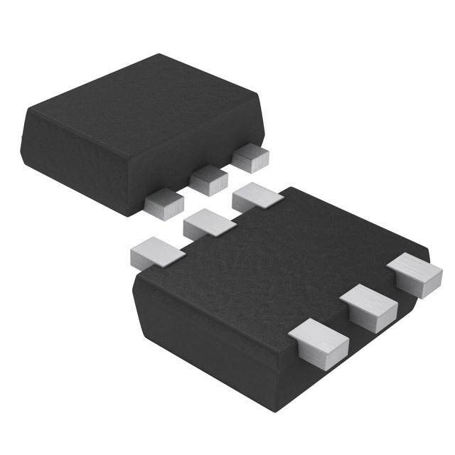
ICGOO电子元器件商城为您提供FDML7610S由Fairchild Semiconductor设计生产,在icgoo商城现货销售,并且可以通过原厂、代理商等渠道进行代购。 FDML7610S价格参考¥5.44-¥5.44。Fairchild SemiconductorFDML7610S封装/规格:晶体管 - FET,MOSFET - 阵列, 2 个 N 沟道(双) Mosfet 阵列 30V 12A,17A 800mW,900mW 表面贴装 8-MLP(3x4.5)。您可以下载FDML7610S参考资料、Datasheet数据手册功能说明书,资料中有FDML7610S 详细功能的应用电路图电压和使用方法及教程。
FDML7610S 是一款由 ON Semiconductor(安森美半导体)生产的双通道 N 沟道增强型 MOSFET 阵列,其主要应用场景包括以下几类:

 1. 电源管理
   - FDML7610S 常用于开关电源、负载开关和 DC-DC 转换器等电源管理电路中。由于其低导通电阻(Rds(on)),可以有效降低功率损耗,提高系统效率。
   - 在电池管理系统(BMS)中,该器件可用于控制电流流向,保护电池免受过充或过放的影响。

 2. 电机驱动
   - 适用于小型直流电机或步进电机的驱动电路。通过 PWM 控制信号,MOSFET 可以调节电机的速度和方向。
   - 其双通道设计允许同时控制两个电机或实现 H 桥驱动。

 3. 信号切换
   - 在需要信号切换的应用中(如多路复用器或多路输入选择器),FDML7610S 的低电容和快速开关特性使其成为理想选择。
   - 它可以用于音频信号切换、传感器信号路由或其他低功耗信号处理场景。

 4. 便携式电子设备
   - 由于其小尺寸封装(例如 LLP 或 SOIC 封装),FDML7610S 广泛应用于手机、平板电脑、可穿戴设备和其他空间受限的便携式电子产品中。
   - 用于 USB 端口保护、充电电路控制以及热插拔保护。

 5. 数据通信
   - 在网络设备(如路由器、交换机)中,该器件可用于信号路径的开关控制,确保数据传输的稳定性和可靠性。
   - 其低导通电阻和低栅极电荷特性有助于减少通信过程中的信号失真和延迟。

 6. 工业自动化
   - 在工业控制领域,FDML7610S 可用于固态继电器(SSR)、传感器接口和 PLC 输出控制。
   - 它能够承受较高的电压和电流波动,适合恶劣的工作环境。

 总结
FDML7610S 的主要优势在于其高集成度、低导通电阻和快速开关性能,适用于需要高效功率转换和信号切换的各种应用场景。无论是消费电子、通信设备还是工业控制,这款 MOSFET 阵列都能提供可靠的解决方案。
| 参数 | 数值 |
| 产品目录 | |
| 描述 | MOSFET 2N-CH 30V 12A/17A 8-MLPMOSFET 30V N-Channel PowerTrench |
| 产品分类 | FET - 阵列分离式半导体 |
| FET功能 | 逻辑电平门 |
| FET类型 | 2 个 N 沟道(双) |
| Id-ContinuousDrainCurrent | 30 A |
| Id-连续漏极电流 | 30 A |
| 品牌 | Fairchild Semiconductor |
| 产品手册 | |
| 产品图片 |
|
| rohs | 符合RoHS无铅 / 符合限制有害物质指令(RoHS)规范要求 |
| 产品系列 | 晶体管,MOSFET,Fairchild Semiconductor FDML7610SPowerTrench® |
| 数据手册 | |
| 产品型号 | FDML7610S |
| Pd-PowerDissipation | 2.2 W |
| Pd-功率耗散 | 2.2 W |
| Qg-GateCharge | 20 nC, 43 nC |
| Qg-栅极电荷 | 20 nC, 43 nC |
| RdsOn-Drain-SourceResistance | 7.5 mOhms |
| RdsOn-漏源导通电阻 | 7.5 mOhms |
| Vds-Drain-SourceBreakdownVoltage | 30 V |
| Vds-漏源极击穿电压 | 30 V |
| Vgs-Gate-SourceBreakdownVoltage | +/- 20 V |
| Vgs-栅源极击穿电压 | 20 V |
| 不同Id时的Vgs(th)(最大值) | 3V @ 250µA |
| 不同Vds时的输入电容(Ciss) | 1750pF @ 15V |
| 不同Vgs时的栅极电荷(Qg) | 28nC @ 10V |
| 不同 Id、Vgs时的 RdsOn(最大值) | 7.5 毫欧 @ 12A,10V |
| 产品种类 | MOSFET |
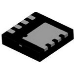
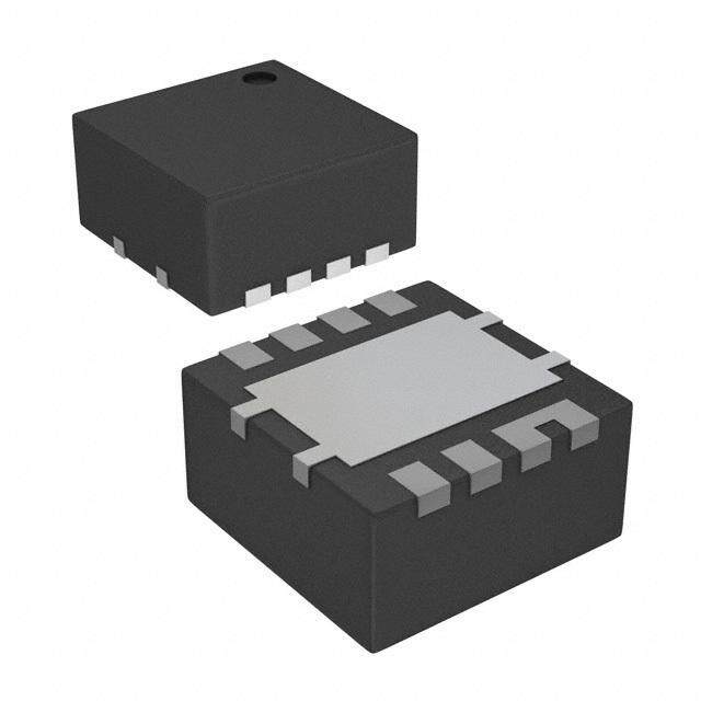
| 供应商器件封装 | 8-MLP(3x4.5) |
| 其它名称 | FDML7610STR |
| 功率-最大值 | 800mW,900mW |
| 包装 | 带卷 (TR) |
| 单位重量 | 300 mg |
| 商标 | Fairchild Semiconductor |
| 安装类型 | 表面贴装 |
| 安装风格 | SMD/SMT |
| 封装 | Reel |
| 封装/外壳 | 8-WDFN 裸露焊盘 |
| 封装/箱体 | MLP-8 3x4.5 |
| 工厂包装数量 | 3000 |
| 晶体管极性 | N-Channel |
| 最大工作温度 | + 150 C |
| 最小工作温度 | - 55 C |
| 标准包装 | 3,000 |
| 漏源极电压(Vdss) | 30V |
| 电流-连续漏极(Id)(25°C时) | 12A,17A |
| 系列 | FDML7610 |
| 配置 | Dual |


- 商务部:美国ITC正式对集成电路等产品启动337调查
- 曝三星4nm工艺存在良率问题 高通将骁龙8 Gen1或转产台积电
- 太阳诱电将投资9.5亿元在常州建新厂生产MLCC 预计2023年完工
- 英特尔发布欧洲新工厂建设计划 深化IDM 2.0 战略
- 台积电先进制程称霸业界 有大客户加持明年业绩稳了
- 达到5530亿美元!SIA预计今年全球半导体销售额将创下新高
- 英特尔拟将自动驾驶子公司Mobileye上市 估值或超500亿美元
- 三星加码芯片和SET,合并消费电子和移动部门,撤换高东真等 CEO
- 三星电子宣布重大人事变动 还合并消费电子和移动部门
- 海关总署:前11个月进口集成电路产品价值2.52万亿元 增长14.8%


PDF Datasheet 数据手册内容提取
Is Now Part of To learn more about ON Semiconductor, please visit our website at www.onsemi.com Please note: As part of the Fairchild Semiconductor integration, some of the Fairchild orderable part numbers will need to change in order to meet ON Semiconductor’s system requirements. Since the ON Semiconductor product management systems do not have the ability to manage part nomenclature that utilizes an underscore (_), the underscore (_) in the Fairchild part numbers will be changed to a dash (-). This document may contain device numbers with an underscore (_). Please check the ON Semiconductor website to verify the updated device numbers. The most current and up-to-date ordering information can be found at www.onsemi.com. Please email any questions regarding the system integration to Fairchild_questions@onsemi.com. ON Semiconductor and the ON Semiconductor logo are trademarks of Semiconductor Components Industries, LLC dba ON Semiconductor or its subsidiaries in the United States and/or other countries. ON Semiconductor owns the rights to a number of patents, trademarks, copyrights, trade secrets, and other intellectual property. A listing of ON Semiconductor’s product/patent coverage may be accessed at www.onsemi.com/site/pdf/Patent-Marking.pdf. ON Semiconductor reserves the right to make changes without further notice to any products herein. ON Semiconductor makes no warranty, representation or guarantee regarding the suitability of its products for any particular purpose, nor does ON Semiconductor assume any liability arising out of the application or use of any product or circuit, and specifically disclaims any and all liability, including without limitation special, consequential or incidental damages. Buyer is responsible for its products and applications using ON Semiconductor products, including compliance with all laws, regulations and safety requirements or standards, regardless of any support or applications information provided by ON Semiconductor. “Typical” parameters which may be provided in ON Semiconductor data sheets and/or specifications can and do vary in different applications and actual performance may vary over time. All operating parameters, including “Typicals” must be validated for each customer application by customer’s technical experts. ON Semiconductor does not convey any license under its patent rights nor the rights of others. ON Semiconductor products are not designed, intended, or authorized for use as a critical component in life support systems or any FDA Class 3 medical devices or medical devices with a same or similar classification in a foreign jurisdiction or any devices intended for implantation in the human body. Should Buyer purchase or use ON Semiconductor products for any such unintended or unauthorized application, Buyer shall indemnify and hold ON Semiconductor and its officers, employees, subsidiaries, affiliates, and distributors harmless against all claims, costs, damages, and expenses, and reasonable attorney fees arising out of, directly or indirectly, any claim of personal injury or death associated with such unintended or unauthorized use, even if such claim alleges that ON Semiconductor was negligent regarding the design or manufacture of the part. ON Semiconductor is an Equal Opportunity/Affirmative Action Employer. This literature is subject to all applicable copyright laws and is not for resale in any manner.
F D M L 7 April 2013 6 1 FDML7610S 0 S ® P PowerTrench Power Stage o w Asymmetric Dual N-Channel MOSFET e r Features General Description T r e Q1: N-Channel This device includes two specialized N-Channel MOSFETs in a n c (cid:132) Max rDS(on) = 7.5 mΩ at VGS = 10 V, ID = 12 A dual MLP package.The switch node has been internally h ® (cid:132) Max rDS(on) = 12 mΩ at VGS = 4.5 V, ID = 10 A connected to enable easy placement and routing of synchronous P buck converters. The control MOSFET (Q1) and synchronous Q2: N-Channel o SyncFETTM (Q2) have been designed to provide optimal power w (cid:132) Max rDS(on) = 4.2 mΩ at VGS = 10 V, ID = 17 A efficiency. er (cid:132) Max rDS(on) = 5.5 mΩ at VGS = 4.5 V, ID = 14 A S Applications t (cid:132) RoHS Compliant a g (cid:132) Computing e (cid:132) Communications (cid:132) General Purpose Point of Load (cid:132) Notebook V CORE D1 D1 Pin 1 D1 G1 D1 S2 5 Q2 4 D1 PHASE (S1/D2) S2 6 PHASE 3 D1 S2 7 2 D1 S2 S2 S2 G2 8 1 G1 G2 Q1 Top MLP 3X4.5 Bottom MOSFET Maximum Ratings TA = 25 °C unless otherwise noted Symbol Parameter Q1 Q2 Units V Drain to Source Voltage 30 30 V DS V Gate to Source Voltage (Note 3) ±20 ±20 V GS Drain Current -Continuous (Package limited) T = 25 °C 30 28 C -Continuous (Silicon limited) T = 25 °C 40 60 I C A D -Continuous T = 25 °C 121a 171b A -Pulsed 40 40 Power Dissipation for Single Operation T = 25 °C 2.11a 2.21b P A W D T = 25 °C 0.81c 0.91d A T , T Operating and Storage Junction Temperature Range -55 to +150 °C J STG Thermal Characteristics R Thermal Resistance, Junction to Ambient 601a 561b θJA R Thermal Resistance, Junction to Ambient 1501c 1401d °C/W θJA R Thermal Resistance, Junction to Case 4 3.5 θJC Package Marking and Ordering Information Device Marking Device Package Reel Size Tape Width Quantity FDML7610S FDML7610S MLP3X4.5 13 ” 12 mm 3000 units ©2013 Fairchild Semiconductor Corporation 1 www.fairchildsemi.com FDML7610S Rev.C1
F D Electrical Characteristics M T = 25 °C unless otherwise noted J L Symbol Parameter Test Conditions Type Min Typ Max Units 7 6 1 Off Characteristics 0 S BV Drain to Source Breakdown Voltage ID = 250 μA, VGS = 0 V Q1 30 V P DSS ID = 1 mA, VGS = 0 V Q2 30 o ΔBV Breakdown Voltage Temperature I = 250 μA, referenced to 25 °C Q1 15 w DSS D mV/°C e ΔT Coefficient I = 10 mA, referenced to 25 °C Q2 14 J D r T Q1 1 μA I Zero Gate Voltage Drain Current V = 24 V, V = 0 V r DSS DS GS Q2 500 μA e n Q1 100 nA c IGSS Gate to Source Leakage Current VGS = 20 V, VDS= 0 V Q2 100 nA h ® P On Characteristics o w V = V , I = 250 μA Q1 1 1.8 3 VGS(th) Gate to Source Threshold Voltage VGGSS = VDDSS, IDD = 1 mA Q2 1 1.8 3 V er ΔV Gate to Source Threshold Voltage I = 250 μA, referenced to 25 °C Q1 -6 S GS(th) D mV/°C t ΔT Temperature Coefficient I = 10 mA, referenced to 25 °C Q2 -5 a J D g VGS = 10 V, ID = 12 A 6.0 7.5 e V = 4.5 V, I = 10 A Q1 8.5 12 GS D V = 10 V, I = 12 A , T = 125 °C 8.3 12 r Drain to Source On Resistance GS D J mΩ DS(on) V = 10 V, I = 17 A 3.2 4.2 GS D V = 4.5 V, I = 14 A Q2 4.1 5.5 GS D V = 10 V, I = 17 A , T = 125 °C 4.1 6 GS D J V = 5 V, I = 12 A Q1 63 g Forward Transconductance DS D S FS V = 5 V, I = 17 A Q2 86 DS D Dynamic Characteristics Q1: Q1 1315 1750 C Input Capacitance pF iss V = 15 V, V = 0 V, f = 1 MHZ Q2 2960 3940 DS GS Q1 455 600 C Output Capacitance pF oss Q2: Q2 1135 1510 VDS = 15 V, VGS = 0 V, f = 1 MHZ Q1 45 70 C Reverse Transfer Capacitance pF rss Q2 100 150 Q1 0.9 R Gate Resistance Ω g Q2 0.6 Switching Characteristics Q1 8.6 18 t Turn-On Delay Time ns d(on) Q1: Q2 13 23 VDD = 15 V, ID = 12 A, Q1 2.5 10 tr Rise Time VGS = 10 V, RGEN = 6 Ω Q2 4 10 ns Q1 20 32 td(off) Turn-Off Delay Time Q2: Q2 31 49 ns V = 15 V, I = 17 A, DD D tf Fall Time VGS = 10 V, RGEN = 6 Ω QQ12 23..31 1100 ns Q1 20 28 Qg Total Gate Charge VGS = 0 V to 10 V Q1 Q2 43 60 nC V = 15 V, DD Q1 9.3 13 Qg Total Gate Charge VGS = 0 V to 4.5 V ID = 12 A Q2 20 28 nC Q1 4.3 Qgs Gate to Source Gate Charge Q2 Q2 8.9 nC V = 15 V, DD Qgd Gate to Drain “Miller” Charge ID = 17A QQ12 24..27 nC ©2013 Fairchild Semiconductor Corporation 2 www.fairchildsemi.com FDML7610S Rev.C1
F D Electrical Characteristics M T = 25 °C unless otherwise noted J L Symbol Parameter Test Conditions Type Min Typ Max Units 7 6 1 Drain-Source Diode Characteristics 0 S V Source to Drain Diode Forward Voltage VGS = 0 V, IS = 12 A (Note 2) Q1 0.8 1.2 V P SD VGS = 0 V, IS = 17 A (Note 2) Q2 0.8 1.2 o Q1 Q1 27 43 w trr Reverse Recovery Time I = 12 A, di/dt = 100 A/μs Q2 35 56 ns e F r Q2 Q1 10 18 T Q Reverse Recovery Charge nC r rr IF = 17 A, di/dt = 300 A/μs Q2 40 64 e n c h Notes: 1: RθJA is determined with the device mounted on a 1 in2 pad 2 oz copper pad on a 1.5 x 1.5 in. board of FR-4 material. RθJC is guaranteed by design while RθCA is determined ® by the user's board design. P o a . 6a0 1 ° iCn2/W p wadh eonf m2 oouzn tceodp opne r b . 5a 61 °iCn2/W p wadh eonf m2 oouzn tceodp opne r we r S t a g e c. 150 °C/W when mounted on a d. 140 °C/W when mounted on a minimum pad of 2 oz copper minimum pad of 2 oz copper 2: Pulse Test: Pulse Width < 300 μs, Duty cycle < 2.0%. 3: As an N-ch device, the negative Vgs rating is for low duty cycle pulse ocurrence only. No continuous rating is implied. ©2013 Fairchild Semiconductor Corporation 3 www.fairchildsemi.com FDML7610S Rev.C1
F D Typical Characteristics (Q1 N-Channel) M T = 25 °C unless otherwise noted J L 7 6 40 4 1 VGS = 10 V CE PULSE DURATION = 80 μs 0S T (A) 30 VGSV =G S 4 .=5 6V V ESISTAN 3 VGS = 3.5 V DUTY CYCLE = 0.5% MAX Pow N DR N CURRE 20 VGS = 4 V ORMALIZEURCE ON- 2 VGS = 4 V VGS = 4.5 V erTren DRAI 10 NO SO 1 ch I, D VGS = 3.5 V PDUULTSYE C DYUCRLEA T=I O0.N5 %= 8M0A μXs AIN T VGS = 6 V VGS = 10 V P® 0 DR 0 ow 0.0 0.5 1.0 1.5 2.0 0 10 20 30 40 e VDS, DRAIN TO SO URCE VOLTAGE (V) ID, DRAIN CURR ENT (A) r S Figure 1. On Region Characteristics Figure 2. Normalized On-Resistance t a vs Drain Current and Gate Voltage g e 1.6 40 STANCE 1.4 IVDG =S 1=2 1 A0 V ()E mΩ 30 PDUULTSYE C DYUCRLEA T=I O0.N5 %= 8M0A μXs NORMALIZED O SOURCE ON-RESI 11..02 rDRAIN TO ,DS(on)RCE ON-RESISTANC 1200 TJ = 125 oC ID = 12 A T U N O AI S TJ = 25 oC R D 0.8-75 -50 -25 0 25 50 75 100 125 150 02 4 6 8 10 TJ, JUNCTION TEM PERATURE (oC) VGS, GATE TO SOURCE VOLTAGE (V) Figure 3. Normalized On Resistance Figure 4. On-Resistance vs Gate to vs Junction Temperature Source Voltage 40 40 PULSE DURATION = 80 μs A) VGS = 0 V DUTY CYCLE = 0.5% MAX T ( 10 N A) 30 RE RRENT ( 20 VDS = 5 V TJ = 150 oC AIN CUR 1 TJ = 150 oC U R AIN C TJ = 25 oC RSE D 0.1 TJ = 25 oC R E D 10 V , D RE 0.01 I TJ = -55 oC I, S TJ = -55 oC 0 0.001 1.5 2.0 2.5 3.0 3.5 4.0 0.0 0.2 0.4 0.6 0.8 1.0 1.2 VGS, GATE TO SOU RCE VOLTAGE (V) VSD, BODY DIODE FOR WARD VOLTAGE (V) Figure 5. Transfer Characteristics Figure 6. Source to Drain Diode Forward Voltage vs Source Current ©2013 Fairchild Semiconductor Corporation 4 www.fairchildsemi.com FDML7610S Rev.C1
F D Typical Characteristics (Q1 N-Channel) M T = 25 °C unless otherwise noted J L 7 6 10 2000 1 V) ID = 12 A 0 E ( 1000 Ciss S AG 8 P LT VDD = 10 V F) o O p w SOURCE V 46 VDD = 15 V CITANCE ( 100 Coss erTre TE TO 2 VDD = 20 V CAPA nch V, GAGS 0 10 fV =G S1 =M 0H Vz Crss Po® 0 5 10 15 20 0.1 1 10 30 w Qg, GATE CH ARGE (nC) VDS, DRAIN TO SOU RCE VOLTAGE (V) er S Figure 7. Gate Charge Characteristics Figure 8. Capacitance vs Drain t a to Source Voltage g e 60 100 VGS = 10 V RθJC = 4 oC/W 100us RENT (A) 40 ENT (A) 10 1 ms , IDRAIN CURD20 VLGimS i=te 4d.5 b Vy Package I, DRAIN CURRD 0.11 RTLSTHIJIθMN JI=SIAGT MAE=L RDAE1E X 5BPA 0YRU I oASLrCD ST/SWEE(Don) 1D111000sC0s m mss TA = 25 oC 0 0.01 25 50 75 100 125 150 0.01 0.1 1 10 100 200 TC, CASE TEMPERATURE (oC) VDS, DRAIN to SOU RCE VOLTAGE (V) Figure 9. Maximum Continuous Drain Current vs Figure 10. Forward Bias Safe Operating Area Case Temperature 1000 W) SINGLE PULSE R ( RθJA = 150 oC/W WE 100 TA = 25 oC O P T N E NSI A 10 R T K A E P , PK) 1 P( 0.5 10-4 10-3 10-2 10-1 1 10 100 1000 t, PULSE WIDTH ( s) Figure 11. Single Pulse Maximum Power Dissipation ©2013 Fairchild Semiconductor Corporation 5 www.fairchildsemi.com FDML7610S Rev.C1
F D Typical Characteristics (Q1 N-Channel) M T = 25 °C unless otherwise noted J L 7 6 2 1 DUTY CYCLE-DESCENDING ORDER 0 1 S D = 0.5 P AL 0.2 o M A 0.1 w ERZJθ 0.1 0.05 e D TH NCE, 00..0021 PDM rTr LIZEEDA en ORMAIMP 0.01 SINGLE PULSE t1t2 ch® N R = 150 oC/W NOTES: θJA DUTY FACTOR: D = t1/t2 P (Note 1c) PEAK TJ = PDM x ZθJA x RθJA + TA o w 0.001 e 10-4 10-3 10-2 10-1 1 10 100 1000 r S t, RECTANGULAR PULSE DURATION (sec) t a Figure 12. Junction-to-Ambient Transient Thermal Response Curve g e ©2013 Fairchild Semiconductor Corporation 6 www.fairchildsemi.com FDML7610S Rev.C1
F D Typical Characteristics (Q2 N-Channel) T = 25 oC unlenss otherwise noted M J L 7 6 40 6 1 E PULSE DURATION = 80 μs 0 T (A) 30 VGSV =G S 4 =.5 1V0 V ESISTANC 45 VGS = 3 V DUTY CYCLE = 0.5% MAX S Pow N DR DRAIN CURRE 1200 VGS =V G 3S.5 = V 4 V NORMALIZEO SOURCE ON- 23 VGS = 3.5 V erTrench I, D VGS = 3 V PDUULTSYE C DYUCRLEA T=I O0.N5 %= 8M0A μXs RAIN T 1 VGS = 4 V VGS = 4.5 V VGS = 10 V P® 0 D 0 o w 0.0 0.2 0.4 0.6 0.8 0 10 20 30 40 e VDS, DRAIN TO SO URCE VOLTAGE (V) ID, DRAIN CURR ENT (A) r S Figure 13. On-Region Characteristics Figure 14. Normalized on-Resistance vs Drain t a Current and Gate Voltage g e 1.6 20 E ID = 17 A PULSE DURATION = 80 μs NC VGS = 10 V )Ω ID = 17 A DUTY CYCLE = 0.5% MAX A 1.4 m ST (E 15 ALIZEDE ON-RESI 1.2 DRAIN TO ESISTANC10 NORM N TO SOURC 01..80 r,DS(on)OURCE ON-R 5 TJ = 125 oC RAI S TJ = 25 oC D 0.6 0 -75 -50 -25 0 25 50 75 100 125 150 2 4 6 8 10 TJ, JUNCTION TEM PERATURE (oC) VGS, GATE TO SOURCE VOLTAGE (V) Figure 15. Normalized On-Resistance Figure 16. On-Resistance vs Gate to vs Junction Temperature Source Voltage 40 40 PULSE DURATION = 80 μs A) VGS = 0 V DUTY CYCLE = 0.5% MAX T ( 10 A) 30 VDS = 5 V REN T ( UR TJ = 125 oC RREN 20 TJ = 125 oC AIN C 1 U R AIN C TJ = 25 oC RSE D TJ = 25 oC R E 0.1 D 10 V , D RE I TJ = -55 oC I, S TJ = -55 oC 0 0.01 1.5 2.0 2.5 3.0 3.5 0.0 0.2 0.4 0.6 0.8 1.0 1.2 VGS, GATE TO SOU RCE VOLTAGE (V) VSD, BODY DIODE FOR WARD VOLTAGE (V) Figure 17. Transfer Characteristics Figure 18. Source to Drain Diode Forward Voltage vs Source Current ©2013 Fairchild Semiconductor Corporation 7 www.fairchildsemi.com FDML7610S Rev.C1
F D M Typical Characteristics (Q2 N-Channel) TJ = 25 oC unless otherwise noted L 7 6 10 5000 1 V) ID = 17A 0S E ( TAG 8 Ciss Po RCE VOL 6 VDD = 10 V NCE (pF)1000 Coss werT E TO SOU 4 VDD = 20 VVDD = 15 V CAPACITA rench AT 2 ® G V, GS 0 10600 fV =G S1 =M 0H Vz Crss Pow 0 10 20 30 40 50 0.1 1 10 30 e Qg, GATE CH ARGE (nC) VDS, DRAIN TO SOU RCE VOLTAGE (V) r S Figure 19. Gate Charge Characteristics Figure 20. Capacitance vs Drain ta to Source Voltage g e 80 100 VGS = 10 V RθJC = 3.5 oC/W ENT (A) 60 NT (A) 10 1 ms , IDRAIN CURRD2400 LimitVeGd Sb =y p4.a5c Vkage I, DRAIN CURRED 0.11 TLRSTHIJIθMN JI=SIAGT MAE=LRD AE1E X 4BPA 0YRU I oSArLCD ST/SWEE(oDn) 1111s000 0sm mss TA = 25 oC DC 0 0.01 25 50 75 100 125 150 0.01 0.1 1 10 100200 TC, CASE TEMPERATURE (oC) VDS, DRAIN to SOU RCE VOLTAGE (V) Figure 21. Maximun Continuous Drain Figure 22. Forward Bias Safe Current vs Case Temperature Operating Area 300 SINGLE PULSE W) RθJA = 140 oC/W ER ( 100 TA = 25 oC W O P T N E SI N A 10 R T K A E P , )K P P( 1 0.001 0.01 0.1 1 10 100 1000 t, PULSE WIDTH (s ec) Figure 23. Single Pulse Maximum Power Dissipation ©2013 Fairchild Semiconductor Corporation 8 www.fairchildsemi.com FDML7610S Rev.C1
F D Typical Characteristics (Q2 N-Channel) T = 25 oC unless otherwise noted M J L 7 6 1 0 S 2 DUTY CYCLE-DESCENDING ORDER P 1 o w D = 0.5 AL 0.2 er M A 0.1 T D THER NCE,ZJθ 0.1 000...000521 PDM renc LIZEEDA h® ORMAIMP 0.01 SINGLE PULSE t1t2 Po N R = 140 oC/W NOTES: w NoθJtAe 1d DPEUATYK FTAJ C= TPODRM: xD Z =θ JtA1 /xt2 RθJA + TA er 0.001 S 10-3 10-2 10-1 1 10 100 1000 ta g t, RECTANGULAR PULSE DURATION (sec) e Figure24. Junction-to-Ambient Transient Thermal Response Curve ©2013 Fairchild Semiconductor Corporation 9 www.fairchildsemi.com FDML7610S Rev.C1
F D Typical Characteristics (continued) M L 7 6 1 SyncFETTM Schottky body diode 0 S Characteristics P o Fairchild’s SyncFETTM process embeds a Schottky diode in Schottky barrier diodes exhibit significant leakage at high tem- w parallel with PowerTrench MOSFET. This diode exhibits similar perature and high reverse voltage. This will increase the power e r characteristics to a discrete external Schottky diode in parallel in the device. T r with a MOSFET. Figure 25 shows the reverse recovery e n characteristic of the FDML7610S. c h ® P 20 10000 o A) w T ( e 15 REN 1000 TJ = 125 oC r S NT (A) 10 di/dt = 300 A/μs AGE CUR 100 TJ = 100 oC tage E K R A R 5 E U L C E S R 10 0 EVE TJ = 25 oC R , S -5 DS 1 0 50 100 150 200 250 I 0 5 10 15 20 25 30 TIME (ns) VDS, REVERSE VOLTAGE (V) Figure 25. FDML7610S SyncFETTM body Figure 26. SyncFETTM body diode reverse diode reverse recovery characteristic leakage versus drain-source voltage ©2013 Fairchild Semiconductor Corporation 10 www.fairchildsemi.com FDML7610S Rev.C1
F D Application Information M L 7 1. Switch Node Ringing Suppression 6 1 Fairchild’s Power Stage products incorporate a proprietary design* that minimizes the peak overshoot, ringing voltage on the switch 0 node (PHASE) without the need of any external snubbing components in a buck converter. As shown in the figure 29, the Power Stage S solution rings significantly less than competitor solutions under the same set of test conditions. P o w e r T r e n c h ® P o w e r S t a g e Power Stage Device Competitors solution Figure 29. Power Stage phase node rising edge, High Side Turn on *Patent Pending ©2013 Fairchild Semiconductor Corporation 11 www.fairchildsemi.com FDML7610S Rev.C1
F D M L 7 6 1 0 S P o w e r T r e n c h ® P o w e r S t a g e Figure 30. Shows the Power Stage in a buck converter topology 2. Recommended PCB Layout Guidelines As a PCB designer, it is necessary to address critical issues in layout to minimize losses and optimize the performance of the power train. Power Stage is a high power density solution and all high current flow paths, such as VIN (D1), PHASE (S1/D2) and GND (S2), should be short and wide for better and stable current flow, heat radiation and system performance. A recommended layout proce- dure is discussed below to maximize the electrical and thermal performance of the part. Figure 31. Recommended PCB Layout ©2013 Fairchild Semiconductor Corporation 12 www.fairchildsemi.com FDML7610S Rev.C1
F D Following is a guideline, not a requirement which the PCB designer should consider: M L 7 1. Input ceramic bypass capacitors C1 and C2 must be placed close to the D1 and S2 pins of Power Stage to help reduce parasitic 6 inductance and high frequency conduction loss induced by switching operation. C1 and C2 show the bypass capacitors placed close 1 0 to the part between D1 and S2. Input capacitors should be connected in parallel close to the part. Multiple input caps can be connected S depending upon the application. P o 2. The PHASE copper trace serves two purposes; In addition to being the current path from the Power Stage package to the output w inductor (L), it also serves as heat sink for the lower FET in the Power Stage package. The trace should be short and wide enough to e r present a low resistance path for the high current flow between the Power Stage and the inductor. This is done to minimize conduction T losses and limit temperature rise. Please note that the PHASE node is a high voltage and high frequency switching node with high re noise potential. Care should be taken to minimize coupling to adjacent traces. The reference layout in figure 31 shows a good balance n c between the thermal and electrical performance of Power Stage. h ® 3. Output inductor location should be as close as possible to the Power Stage device for lower power loss due to copper trace P resistance. A shorter and wider PHASE trace to the inductor reduces the conduction loss. Preferably the Power Stage should be o w directly in line (as shown in figure 31) with the inductor for space savings and compactness. e r 4. The PowerTrench® Technology MOSFETs used in the Power Stage are effective at minimizing phase node ringing. It allows the S part to operate well within the breakdown voltage limits. This eliminates the need to have an external snubber circuit in most cases. If ta the designer chooses to use an RC snubber, it should be placed close to the part between the PHASE pad and S2 pins to dampen g e the high-frequency ringing. 5. The driver IC should be placed close to the Power Stage part with the shortest possible paths for the High Side gate and Low Side gates through a wide trace connection. This eliminates the effect of parasitic inductance and resistance between the driver and the MOSFET and turns the devices on and off as efficiently as possible. At higher-frequency operation this impedance can limit the gate current trying to charge the MOSFET input capacitance. This will result in slower rise and fall times and additional switching losses. Power Stage has both the gate pins on the same side of the package which allows for back mounting of the driver IC to the board. This provides a very compact path for the drive signals and improves efficiency of the part. 6. S2 pins should be connected to the GND plane with multiple vias for a low impedance grounding. Poor grounding can create a noise transient offset voltage level between S2 and driver ground. This could lead to faulty operation of the gate driver and MOSFET. 7. Use multiple vias on each copper area to interconnect top, inner and bottom layers to help smooth current flow and heat conduction. Vias should be relatively large, around 8 mils to 10 mils, and of reasonable inductance. Critical high frequency components such as ceramic bypass caps should be located close to the part and on the same side of the PCB. If not feasible, they should be connected from the backside via a network of low inductance vias. ©2013 Fairchild Semiconductor Corporation 13 www.fairchildsemi.com FDML7610S Rev.C1
None
ON Semiconductor and are trademarks of Semiconductor Components Industries, LLC dba ON Semiconductor or its subsidiaries in the United States and/or other countries. ON Semiconductor owns the rights to a number of patents, trademarks, copyrights, trade secrets, and other intellectual property. A listing of ON Semiconductor’s product/patent coverage may be accessed at www.onsemi.com/site/pdf/Patent−Marking.pdf. ON Semiconductor reserves the right to make changes without further notice to any products herein. ON Semiconductor makes no warranty, representation or guarantee regarding the suitability of its products for any particular purpose, nor does ON Semiconductor assume any liability arising out of the application or use of any product or circuit, and specifically disclaims any and all liability, including without limitation special, consequential or incidental damages. Buyer is responsible for its products and applications using ON Semiconductor products, including compliance with all laws, regulations and safety requirements or standards, regardless of any support or applications information provided by ON Semiconductor. “Typical” parameters which may be provided in ON Semiconductor data sheets and/or specifications can and do vary in different applications and actual performance may vary over time. All operating parameters, including “Typicals” must be validated for each customer application by customer’s technical experts. ON Semiconductor does not convey any license under its patent rights nor the rights of others. ON Semiconductor products are not designed, intended, or authorized for use as a critical component in life support systems or any FDA Class 3 medical devices or medical devices with a same or similar classification in a foreign jurisdiction or any devices intended for implantation in the human body. Should Buyer purchase or use ON Semiconductor products for any such unintended or unauthorized application, Buyer shall indemnify and hold ON Semiconductor and its officers, employees, subsidiaries, affiliates, and distributors harmless against all claims, costs, damages, and expenses, and reasonable attorney fees arising out of, directly or indirectly, any claim of personal injury or death associated with such unintended or unauthorized use, even if such claim alleges that ON Semiconductor was negligent regarding the design or manufacture of the part. ON Semiconductor is an Equal Opportunity/Affirmative Action Employer. This literature is subject to all applicable copyright laws and is not for resale in any manner. PUBLICATION ORDERING INFORMATION LITERATURE FULFILLMENT: N. American Technical Support: 800−282−9855 Toll Free ON Semiconductor Website: www.onsemi.com Literature Distribution Center for ON Semiconductor USA/Canada 19521 E. 32nd Pkwy, Aurora, Colorado 80011 USA Europe, Middle East and Africa Technical Support: Order Literature: http://www.onsemi.com/orderlit Phone: 303−675−2175 or 800−344−3860 Toll Free USA/Canada Phone: 421 33 790 2910 Fax: 303−675−2176 or 800−344−3867 Toll Free USA/Canada Japan Customer Focus Center For additional information, please contact your local Email: orderlit@onsemi.com Phone: 81−3−5817−1050 Sales Representative © Semiconductor Components Industries, LLC www.onsemi.com www.onsemi.com 1
Mouser Electronics Authorized Distributor Click to View Pricing, Inventory, Delivery & Lifecycle Information: O N Semiconductor: FDML7610S