ICGOO在线商城 > 分立半导体产品 > 晶体管 - FET,MOSFET - 单 > FCPF190N60E

 Datasheet下载
- 型号: FCPF190N60E
- 制造商: Fairchild Semiconductor
- 库位|库存: xxxx|xxxx
- 要求:
| 数量阶梯 | 香港交货 | 国内含税 |
| +xxxx | $xxxx | ¥xxxx |
查看当月历史价格
查看今年历史价格
FCPF190N60E产品简介:
ICGOO电子元器件商城为您提供FCPF190N60E由Fairchild Semiconductor设计生产,在icgoo商城现货销售,并且可以通过原厂、代理商等渠道进行代购。 FCPF190N60E价格参考¥14.20-¥34.13。Fairchild SemiconductorFCPF190N60E封装/规格:晶体管 - FET,MOSFET - 单, 通孔 N 沟道 600V 20.6A(Tc) 39W(Tc) TO-220F-3。您可以下载FCPF190N60E参考资料、Datasheet数据手册功能说明书,资料中有FCPF190N60E 详细功能的应用电路图电压和使用方法及教程。
ON Semiconductor的FCPF190N60E是一款增强型N沟道MOSFET(金属氧化物场效应晶体管),广泛应用于各种电力电子设备中。该器件具有600V的击穿电压(BVdss)和极低的导通电阻(Rds(on)),使其适用于高效率、高可靠性的开关电源和电机驱动等应用。

 主要应用场景:

1. 开关电源 (SMPS):
   FCPF190N60E常用于开关电源中的功率级,如AC-DC转换器、DC-DC转换器等。其高耐压和低导通电阻特性有助于提高转换效率,减少功率损耗,特别是在高频开关条件下表现尤为出色。

2. 电机驱动:
   该MOSFET适用于无刷直流电机(BLDC)、步进电机和其他类型的电机驱动电路。其快速开关速度和低导通电阻可以有效降低发热,延长电机寿命,并提高系统的整体性能。

3. 太阳能逆变器:
   在太阳能光伏发电系统中,FCPF190N60E可用于逆变器模块,将直流电转换为交流电。其高耐压特性和高效的开关性能确保了逆变器在恶劣环境下的稳定运行。

4. 电动车辆 (EV) 和混合动力车辆 (HEV):
   该MOSFET可用于电动汽车和混合动力汽车的电池管理系统(BMS)、电机控制器和充电系统中。其出色的电气特性有助于提升车辆的能效和可靠性。

5. 工业自动化:
   在工业自动化领域,FCPF190N60E可用于伺服驱动器、可编程逻辑控制器(PLC)和其他控制设备中。其高可靠性和耐用性使得它能够在严苛的工业环境中长期稳定工作。

6. 不间断电源 (UPS):
   FCPF190N60E也可用于UPS系统中,提供高效的电力备份和保护功能。其快速响应能力和低功耗特性有助于提高UPS系统的效率和稳定性。

总之,FCPF190N60E凭借其优异的电气性能和可靠性,成为众多电力电子应用的理想选择,特别适合需要高效、高可靠性的开关和驱动场合。
| 参数 | 数值 |
| 产品目录 | |
| 描述 | MOSFET N-CH 600V TO-220-3 |
| 产品分类 | FET - 单 |
| FET功能 | 标准 |
| FET类型 | MOSFET N 通道,金属氧化物 |
| 品牌 | Fairchild Semiconductor |
| 数据手册 | |
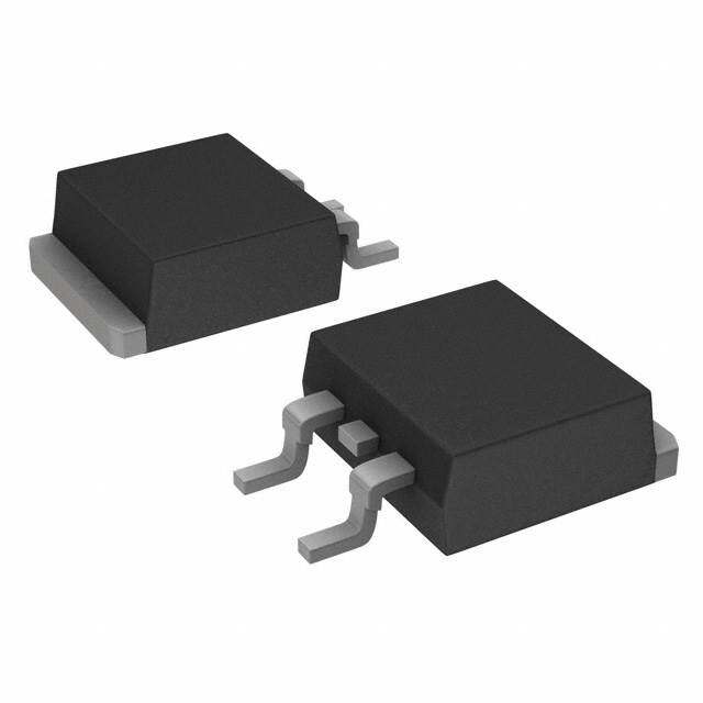
| 产品图片 |
|
| 产品型号 | FCPF190N60E |
| PCN封装 | |
| PCN组件/产地 | |
| rohs | 无铅 / 符合限制有害物质指令(RoHS)规范要求 |
| 产品系列 | SuperFETII® |
| 不同Id时的Vgs(th)(最大值) | 3.5V @ 250µA |
| 不同Vds时的输入电容(Ciss) | 3175pF @ 25V |
| 不同Vgs时的栅极电荷(Qg) | 82nC @ 10V |
| 不同 Id、Vgs时的 RdsOn(最大值) | 190 毫欧 @ 10A,10V |
| 供应商器件封装 | TO-220F |
| 功率-最大值 | 39W |
| 包装 | 管件 |
| 安装类型 | 通孔 |
| 封装/外壳 | TO-220-3 整包 |
| 标准包装 | 50 |
| 漏源极电压(Vdss) | 600V |
| 特色产品 | http://www.digikey.cn/product-highlights/cn/zh/fairchild-semiconductor-superfet-mosfets/4170http://www.digikey.cn/product-highlights/cn/zh/fairchild-cloud-systems-computing/4301 |
| 电流-连续漏极(Id)(25°C时) | 20.6A (Tc) |


- 商务部:美国ITC正式对集成电路等产品启动337调查
- 曝三星4nm工艺存在良率问题 高通将骁龙8 Gen1或转产台积电
- 太阳诱电将投资9.5亿元在常州建新厂生产MLCC 预计2023年完工
- 英特尔发布欧洲新工厂建设计划 深化IDM 2.0 战略
- 台积电先进制程称霸业界 有大客户加持明年业绩稳了
- 达到5530亿美元!SIA预计今年全球半导体销售额将创下新高
- 英特尔拟将自动驾驶子公司Mobileye上市 估值或超500亿美元
- 三星加码芯片和SET,合并消费电子和移动部门,撤换高东真等 CEO
- 三星电子宣布重大人事变动 还合并消费电子和移动部门
- 海关总署:前11个月进口集成电路产品价值2.52万亿元 增长14.8%


PDF Datasheet 数据手册内容提取
Is Now Part of To learn more about ON Semiconductor, please visit our website at www.onsemi.com Please note: As part of the Fairchild Semiconductor integration, some of the Fairchild orderable part numbers will need to change in order to meet ON Semiconductor’s system requirements. Since the ON Semiconductor product management systems do not have the ability to manage part nomenclature that utilizes an underscore (_), the underscore (_) in the Fairchild part numbers will be changed to a dash (-). This document may contain device numbers with an underscore (_). Please check the ON Semiconductor website to verify the updated device numbers. The most current and up-to-date ordering information can be found at www.onsemi.com. Please email any questions regarding the system integration to Fairchild_questions@onsemi.com. ON Semiconductor and the ON Semiconductor logo are trademarks of Semiconductor Components Industries, LLC dba ON Semiconductor or its subsidiaries in the United States and/or other countries. ON Semiconductor owns the rights to a number of patents, trademarks, copyrights, trade secrets, and other intellectual property. A listing of ON Semiconductor’s product/patent coverage may be accessed at www.onsemi.com/site/pdf/Patent-Marking.pdf. ON Semiconductor reserves the right to make changes without further notice to any products herein. ON Semiconductor makes no warranty, representation or guarantee regarding the suitability of its products for any particular purpose, nor does ON Semiconductor assume any liability arising out of the application or use of any product or circuit, and specifically disclaims any and all liability, including without limitation special, consequential or incidental damages. Buyer is responsible for its products and applications using ON Semiconductor products, including compliance with all laws, regulations and safety requirements or standards, regardless of any support or applications information provided by ON Semiconductor. “Typical” parameters which may be provided in ON Semiconductor data sheets and/or specifications can and do vary in different applications and actual performance may vary over time. All operating parameters, including “Typicals” must be validated for each customer application by customer’s technical experts. ON Semiconductor does not convey any license under its patent rights nor the rights of others. ON Semiconductor products are not designed, intended, or authorized for use as a critical component in life support systems or any FDA Class 3 medical devices or medical devices with a same or similar classification in a foreign jurisdiction or any devices intended for implantation in the human body. Should Buyer purchase or use ON Semiconductor products for any such unintended or unauthorized application, Buyer shall indemnify and hold ON Semiconductor and its officers, employees, subsidiaries, affiliates, and distributors harmless against all claims, costs, damages, and expenses, and reasonable attorney fees arising out of, directly or indirectly, any claim of personal injury or death associated with such unintended or unauthorized use, even if such claim alleges that ON Semiconductor was negligent regarding the design or manufacture of the part. ON Semiconductor is an Equal Opportunity/Affirmative Action Employer. This literature is subject to all applicable copyright laws and is not for resale in any manner.
F C P 1 9 December 2014 0 N 6 FCP190N60E / FCPF190N60E 0 E N-Channel SuperFET® II Easy-Drive MOSFET / F C P 600 V, 20.6 A, 190 mΩ F 1 9 Features Description 0 N • 650 V @ T = 150°C SuperFET® II MOSFET is Fairchild Semiconductor’s brand-new 6 J 0 • Typ. RDS(on) = 160 mΩ high voltage super-junction (SJ) MOSFET family that is utilizing E charge balance technology for outstanding low on-resistance • Ultra Low Gate Charge (Typ. Q = 63 nC) — g and lower gate charge performance. This technology is tailored • Low Effective Output Capacitance (Typ. C = 178 pF) oss(eff.) to minimize conduction loss, provide superior switching perfor- N • 100% Avalanche Tested mance, dv/dt rate and higher avalanche energy. Consequently, -C • An Integrated Gate Resistor SuperFET II MOSFET easy-drive series offers slightly slower h • RoHS Compliant rise and fall times compared to the SuperFET II MOSFET an series. Noted by the "E" part number suffix, this family helps n Applications manage EMI issues and allows for easier design implementa- e l tion. For faster switching in applications where switching losses S • LCD / LED / PDP TV Lighting must be at an absolute minimum, please consider the Super- u • Solar Inverter FET II MOSFET series. p e • AC-DC Power Supply r F E D T ® I I E a s y G - G D D G S TO-220 DS TO-220F ri v e S M MOSFET Maximum Ratings TC = 25oC unless otherwise noted. O S Symbol Parameter FCP190N60E FCPF190N60E Unit F V Drain to Source Voltage 600 V E DSS T - DC ±20 V V Gate to Source Voltage GSS - AC (f > 1 Hz) ±30 V - Continuous (T = 25oC) 20.6 20.6* I Drain Current C A D - Continuous (T = 100oC) 13.1 13.1* C I Drain Current - Pulsed (Note 1) 61.8 61.8* A DM E Single Pulsed Avalanche Energy (Note 2) 400 mJ AS I Avalanche Current (Note 1) 4.0 A AR E Repetitive Avalanche Energy (Note 1) 2.1 mJ AR MOSFET dv/dt 100 dv/dt V/ns Peak Diode Recovery dv/dt (Note 3) 20 (T = 25oC) 208 39 W P Power Dissipation C D - Derate Above 25oC 1.67 0.31 W/oC T , T Operating and Storage Temperature Range -55 to +150 oC J STG T Maximum Lead Temperature for Soldering, 1/8” from Case for 5 Seconds 300 oC L *Drain current limited by maximum junction temperature. Thermal Characteristics Symbol Parameter FCP190N60E FCPF190N60E Unit R Thermal Resistance, Junction to Case, Max. 0.6 3.2 θJC oC/W R Thermal Resistance, Junction to Ambient, Max. 62.5 62.5 θJA ©2011 Fairchild Semiconductor Corporation 1 www.fairchildsemi.com FCP190N60E / FCPF190N60E Rev. C11
F C Package Marking and Ordering Information P 1 9 Part Number Top Mark Package Packing Method Reel Size Tape Width Quantity 0 FCP190N60E FCP190N60E TO-220 Tube N/A N/A 50 units N 6 FCPF190N60E FCPF190N60E TO-220F Tube N/A N/A 50 units 0 E Electrical Characteristics TC = 25oC unless otherwise noted. / F C Symbol Parameter Test Conditions Min. Typ. Max. Unit P F Off Characteristics 1 9 V = 0 V, I = 10 mA, T = 25°C 600 - - 0 BV Drain to Source Breakdown Voltage GS D J V N DSS VGS = 0 V, ID = 10 mA, TJ = 150°C 650 - - 6 ΔBV Breakdown Voltage Temperature 0 DSS I = 10 mA, Referenced to 25oC - 0.67 - V/oC E / ΔTJ Coefficient D — Drain to Source Avalanche Breakdown BVDS Voltage VGS = 0 V, ID = 20 A - 700 - V N I Zero Gate Voltage Drain Current VDS = 600 V, VGS = 0 V - - 1 μA -C DSS V = 480 V, T = 125oC - 2.8 - h DS C a I Gate to Body Leakage Current V = ±20 V, V = 0 V - - ±100 nA n GSS GS DS n e On Characteristics l S VGS(th) Gate Threshold Voltage VGS = VDS, ID = 250 μA 2.5 - 3.5 V u RDS(on) Static Drain to Source On Resistance VGS = 10 V, ID = 10 A - 0.16 0.19 Ω pe g Forward Transconductance V = 20 V, I = 10 A - 20 - S r FS DS D F E Dynamic Characteristics T ® CCiss IOnuptuptu Ct aCpaapcaitcaitnacnece VDS = 25 V, VGS = 0 V, -- 12739855 23319765 ppFF II E oss f = 1 MHz a Crss Reverse Transfer Capacitance - 110 165 pF s C Output Capacitance V = 380 V, V = 0 V, f = 1 MHz - 42 - pF y oss DS GS - D C Effective Output Capacitance V = 0 V to 480 V, V = 0 V - 178 - pF oss(eff.) DS GS r Qg(tot) Total Gate Charge at 10V VDS = 380 V, ID = 10 A, - 63 82 nC ive Qgs Gate to Source Gate Charge VGS = 10 V - 10 - nC M Q Gate to Drain “Miller” Charge (Note 4) - 24 - nC gd O ESR Equivalent Series Resistance f = 1 MHz - 5 - Ω S F Switching Characteristics E T t Turn-On Delay Time - 23 56 ns d(on) tr Turn-On Rise Time VDD = 380 V, ID = 10 A, - 14 38 ns V = 10 V, R = 4.7 Ω t Turn-Off Delay Time GS G - 101 212 ns d(off) tf Turn-Off Fall Time (Note 4) - 15 40 ns Drain-Source Diode Characteristics I Maximum Continuous Drain to Source Diode Forward Current - - 20.2 A S I Maximum Pulsed Drain to Source Diode Forward Current - - 60.6 A SM V Drain to Source Diode Forward Voltage V = 0 V, I = 10 A - - 1.2 V SD GS SD trr Reverse Recovery Time VGS = 0 V, ISD = 10 A, - 308 - ns Qrr Reverse Recovery Charge dIF/dt = 100 A/μs - 4.8 - μC Notes: 1. Repetitive rating : pulse-width limited by maximum junction temperature. 2. IAS = 4 A, VDD = 50 V, RG = 25 Ω, starting TJ = 25°C. 3. ISD ≤ 10 A, di/dt ≤ 200 A/μs, VDD ≤ BVDSS, starting TJ = 25°C. 4. Essentially independent of operating temperature typical characteristics. ©2011 Fairchild Semiconductor Corporation 2 www.fairchildsemi.com FCP190N60E / FCPF190N60E Rev. C11
F C Typical Performance Characteristics P 1 9 0 N Figure 1. On-Region Characteristics Figure 2. Transfer Characteristics 6 0 50 100 E VGS = 15.0V *Notes: / 10.0V 1. VDS = 20V F 8.0V 2. 250μs Pulse Test C 7.0V P I, Drain Current [A]D101 6554....0505VVVV I, Drain Current [A]D10 150oC-55oC25oC F190N60E — *Notes: N 1. 250μs Pulse Test - C 2. TC = 25oC h 0.3 1 a 0.1 1 10 2 3 4 5 6 7 8 n VDS, Drain to Source Voltage[V] VGS, Gate to Source Voltage[V] n e l Figure 3. On-Resistance Variation vs. Figure 4. Body Diode Forward Voltage S Drain Current and Gate Voltage Variation vs. Source Current u p and Temperature e r 0.4 100 F E T ® nce A] II R [],ΩDS(ON)n to Source On-Resista00..23 VGS = 1V0GVS = 20V Reverse Drain Current [ 10 150oC 25oC Easy-Drive MO Drai I, S *1N. oVtes := 0V S 0.1 *Note: TC = 25oC 1 2. 25G0Sμs Pulse Test FE 0 10 20 30 40 50 60 0.2 0.4 0.6 0.8 1.0 1.2 1.4 1.6 T ID, Drain Current [A] VSD, Body Diode Forward Voltage [V] Figure 5. Capacitance Characteristics Figure 6. Gate Charge Characteristics 10000 10 Ciss V] VDS = 120V 1000 e [ 8 VDS = 300V ag VDS = 480V F] olt ces [p 100 Coss urce V 6 n o a S Capacit 10 * N 12o.. tfVe =G: S1 M= H0Vz Crss Gate to 4 , S 2 Ciss = Cgs + Cgd (Cds = shorted) G V Coss = Cds + Cgd 1 Crss = Cgd *Note: ID = 10A 0.5 0 0.1 1 10 100 600 0 15 30 45 60 75 VDS, Drain to Source Voltage [V] Qg, Total Gate Charge [nC] ©2011 Fairchild Semiconductor Corporation 3 www.fairchildsemi.com FCP190N60E / FCPF190N60E Rev. C11
F C Typical Performance Characteristics P (Continued) 1 9 0 N Figure 7. Breakdown Voltage Variation Figure 8. On-Resistance Variation 6 vs. Temperature vs. Temperature 0 E 1.20 3.0 / e F g C olta 1.15 nce 2.5 P V a F malized] akdown 11..0150 malized] n-Resist 2.0 190N BV, [NorDSSDrain to Source Bre 001...990050 * N 1o. tVeGs:S = 0V R, [NorDS(on)Drain to Source O 011...505 * N 1o. tVeGs:S = 10V 60E — N-Ch 2. ID = 10mA 2. ID = 10A a 0.85 0.0 n -100 -50 0 50 100 150 200 -100 -50 0 50 100 150 200 n TJ, Junction Temperature [oC] TJ, Junction Temperature [oC] el S Figure 9. Maximum Safe Operating Area Figure 10. Maximum Safe Operating Area u p for FCP190N60E for FCPF190N60E e r F 100 100 E 10μs T 10μs ® A] 10 1ms100μs A] 10 100μs II E ent [ 10ms ent [ 1ms as I, Drain CurrD 1 Oisp Leirmatitioedn biny TRh DisS (Aonre)a DC I, Drain CurrD 1 Oisp Leirmatitioedn biny TRh DisS (Aonre)a DC10ms y-Drive M 0.1 *Notes: 0.1 *Notes: 1. TC = 25oC 1. TC = 25oC OS 2. TJ = 150oC 2. TJ = 150oC F 3. Single Pulse 3. Single Pulse E 0.01 0.01 T 0.1 1 10 100 1000 0.1 1 10 100 1000 VDS, Drain to Source Voltage [V] VDS, Drain to Source Voltage [V] Figure 11. Maximum Drain Current Figure 12. Eoss vs. Drain to Source Voltage vs. Case Temperature 25 10 20 8 A] Current [ 15 , [J]μSS 6 ain 10 EO 4 Dr , D I 5 2 0 0 25 50 75 100 125 150 TC, Case Temperature [oC] 0 10V0 Dr2a0i0ntoS3o0u0rceV4o0lt0age[V50]0 600 ©2011 Fairchild Semiconductor Corporation 4 www.fairchildsemi.com FCP190N60E / FCPF190N60E Rev. C11
F C Typical Performance Characteristics P (Continued) 1 9 0 N Figure 13. Transient Thermal Response Curve for FCP190N60E 6 0 E 1 / W] F ose [C/Z]JCθ 0.5 CPF hermal Responal Response [ 0.1 000..0.125 PDM t1t2 190N60E Tm *Notes: Z(t), JCθTher 00S..i00n21gle pulse 12.. ZDθuJtCy( tF) a=c 0to.6r,o CD/=W t 1M/t2ax. — N 3. TJM - TC = PDM * ZθJC(t) - 0.01 C 10-5 10-4 10-3 10-2 10-1 1 h Rt1e, cRteacntganuglaurl aPr uPlusles eD Duuraratitoionn [[sseecc]] an n e l Figure 14. Transient Thermal Response Curve for FCPF190N60E S u p e 5 W] rF oonse [C/e Z][JCθ 1 00..25 ETII® hermal Respal Respons 0.1 000..00.152 PDM t1t2 Easy-D (t), ThermC 0.01 * N 1o. tZeθsJ:C(t) = 3.2oC/W Max. riv Z TJθ Single pulse 32.. TDJuMty - FTaCc =to Pr,D DM =* tZ1θ/tJ2C(t) e M 0.01 O 10-5 10-4 10-3 10-2 10-1 1 10 100 S tR1,e Rcteacntagnuglualra Pr Puulslsee D Duurraattiioonn [[sseecc]] F E T ©2011 Fairchild Semiconductor Corporation 5 www.fairchildsemi.com FCP190N60E / FCPF190N60E Rev. C11
F C P 1 9 0 N 6 0 E / F C P F 1 9 0 N 6 0 E — N IG = const. -C h a n n e Figure 15. Gate Charge Test Circuit & Waveform l S u p e r F E T VVDDSS RRLL VVDDSS 9900%% II ® E VVGGSS VVDDDD as RRGG y - D 1100%% r VV i V1100GVVS DDUUTT GGSS ve tt tt tt M dd((oonn)) rr dd((ooffff)) tt ff O tt tt oonn ooffff S Figure 16. Resistive Switching Test Circuit & Waveforms F E T V GS Figure 17. Unclamped Inductive Switching Test Circuit & Waveforms ©2011 Fairchild Semiconductor Corporation 6 www.fairchildsemi.com FCP190N60E / FCPF190N60E Rev. C11
F C P 1 9 0 N 6 0 E / DDUUTT ++ F C P F VVDDSS 1 9 0 __ N 6 0 E II — SSDD LLL N - C h DDrriivveerr a n RR n GG SSaammee TTyyppee e aass DDUUTT VVDDDD l S u p VVGGSS ••ddvv//ddttccoonnttrroolllleedd bbyy RR e GG r F ••II ccoonnttrroolllleedd bbyy ppuullssee ppeerriioodd SSDD E T ® I I E a s y VVGGSS DDD ===------GGGGGG------aaaaaa------tttttt---eeeeee------ PPPPPP------uuu---uuu---llllll---ssssss---eeeeee------ ---WWWPPP------eee---iii---dddrrr---iiitttooo---hhh---ddd--- 1100VV -Dri (( DDrriivveerr )) v e M O S II ,, BBooddyy DDiiooddee FFoorrwwaarrdd CCuurrrreenntt FFMM F II E SSDD T (( DDUUTT )) ddii//ddtt II RRMM BBooddyy DDiiooddee RReevveerrssee CCuurrrreenntt VV DDSS (( DDUUTT )) BBooddyy DDiiooddee RReeccoovveerryyddvv//ddtt VV VV SSDD DDDD BBooddyy DDiiooddee FFoorrwwaarrdd VVoollttaaggee DDrroopp Figure 18. Peak Diode Recovery dv/dt Test Circuit & Waveforms ©2011 Fairchild Semiconductor Corporation 7 www.fairchildsemi.com FCP190N60E / FCPF190N60E Rev. C11
SUPPLIER"B"PACKAGE SHAPE (cid:145)(cid:23)(cid:17)(cid:19)(cid:19) 3.50 10.67 SUPPLIER"A"PACKAGE 9.65 E SHAPE 3.40 2.50 16.30 IFPRESENT,SEENOTE"D" 13.90 E 16.51 9.40 15.42 8.13 E 1 2 3 2.46 4.10 C 2.70 14.04 2.13 12.70 2.06 FRONTVIEWS 4.70 1.62 1.62 4.00 1.42H 2.67 1.10 2.40 "A1" 8.65 1.00 SEENOTE"F" 7.59 0.55 (cid:24)(cid:131) (cid:24)(cid:131) OPTIONAL 6.69 (cid:22)(cid:131) (cid:22)(cid:131) 6.06 CHAMFER E 14.30 11.50 NOTE"I" BOTTOMVIEW NOTES: A)REFERENCEJEDEC,TO-220,VARIATIONAB B)ALLDIMENSIONSAREINMILLIMETERS. C)DIMENSIONSCOMMONTOALLPACKAGE SUPPLIERSEXCEPTWHERENOTED. 3 2 1 D)LOCATIONOFMOLDEDFEATUREMAYVARY (LOWERLEFTCORNER,LOWERCENTER ANDCENTEROFTHEPACKAGE) EDOESNOTCOMPLYJEDECSTANDARDVALUE. F)"A1"DIMENSIONSASBELOW: SINGLEGAUGE=0.51-0.61 DUALGAUGE=1.10-1.45 G)DRAWINGFILENAME:TO220B03REV9 HPRESENCEISSUPPLIERDEPENDENT I)SUPPLIERDEPENDENTMOLDLOCKINGHOLES INHEATSINK. 0.60 0.36 2.85 BACKVIEW 2.10 SIDEVIEW
10.36 2.66 A B B 9.96 2.42 3.28 3.40 7.00 3.08 0.70 3.20 SEE NOTE "F" SEE NOTE "F" 6.88 6.48 1 X 45° 16.07 B 15.67 16.00 15.60 (3.23) B 3 1 1.47 2.96 2.14 1.24 2.56 0.90 10.05 0.70 9.45 0.50 M A 30° 0.45 0.60 0.25 B 0.45 2.54 2.54 4.90 B 4.50 NOTES: A. EXCEPT WHERE NOTED CONFORMS TO EIAJ SC91A. B DOES NOT COMPLY EIAJ STD. VALUE. C. ALL DIMENSIONS ARE IN MILLIMETERS. D. DIMENSIONS ARE EXCLUSIVE OF BURRS, MOLD FLASH AND TIE BAR PROTRUSIONS. E. DIMENSION AND TOLERANCE AS PER ASME Y14.5-1994. F. OPTION 1 - WITH SUPPORT PIN HOLE. OPTION 2 - NO SUPPORT PIN HOLE. G. DRAWING FILE NAME: TO220M03REV5
ON Semiconductor and are trademarks of Semiconductor Components Industries, LLC dba ON Semiconductor or its subsidiaries in the United States and/or other countries. ON Semiconductor owns the rights to a number of patents, trademarks, copyrights, trade secrets, and other intellectual property. A listing of ON Semiconductor’s product/patent coverage may be accessed at www.onsemi.com/site/pdf/Patent−Marking.pdf. ON Semiconductor reserves the right to make changes without further notice to any products herein. ON Semiconductor makes no warranty, representation or guarantee regarding the suitability of its products for any particular purpose, nor does ON Semiconductor assume any liability arising out of the application or use of any product or circuit, and specifically disclaims any and all liability, including without limitation special, consequential or incidental damages. Buyer is responsible for its products and applications using ON Semiconductor products, including compliance with all laws, regulations and safety requirements or standards, regardless of any support or applications information provided by ON Semiconductor. “Typical” parameters which may be provided in ON Semiconductor data sheets and/or specifications can and do vary in different applications and actual performance may vary over time. All operating parameters, including “Typicals” must be validated for each customer application by customer’s technical experts. ON Semiconductor does not convey any license under its patent rights nor the rights of others. ON Semiconductor products are not designed, intended, or authorized for use as a critical component in life support systems or any FDA Class 3 medical devices or medical devices with a same or similar classification in a foreign jurisdiction or any devices intended for implantation in the human body. Should Buyer purchase or use ON Semiconductor products for any such unintended or unauthorized application, Buyer shall indemnify and hold ON Semiconductor and its officers, employees, subsidiaries, affiliates, and distributors harmless against all claims, costs, damages, and expenses, and reasonable attorney fees arising out of, directly or indirectly, any claim of personal injury or death associated with such unintended or unauthorized use, even if such claim alleges that ON Semiconductor was negligent regarding the design or manufacture of the part. ON Semiconductor is an Equal Opportunity/Affirmative Action Employer. This literature is subject to all applicable copyright laws and is not for resale in any manner. PUBLICATION ORDERING INFORMATION LITERATURE FULFILLMENT: N. American Technical Support: 800−282−9855 Toll Free ON Semiconductor Website: www.onsemi.com Literature Distribution Center for ON Semiconductor USA/Canada 19521 E. 32nd Pkwy, Aurora, Colorado 80011 USA Europe, Middle East and Africa Technical Support: Order Literature: http://www.onsemi.com/orderlit Phone: 303−675−2175 or 800−344−3860 Toll Free USA/Canada Phone: 421 33 790 2910 Fax: 303−675−2176 or 800−344−3867 Toll Free USA/Canada Japan Customer Focus Center For additional information, please contact your local Email: orderlit@onsemi.com Phone: 81−3−5817−1050 Sales Representative © Semiconductor Components Industries, LLC www.onsemi.com www.onsemi.com 1
Mouser Electronics Authorized Distributor Click to View Pricing, Inventory, Delivery & Lifecycle Information: O N Semiconductor: FCPF190N60E