ICGOO在线商城 > 分立半导体产品 > 晶体管 - FET,MOSFET - 单 > STD150N3LLH6
 Datasheet下载
- 型号: STD150N3LLH6
- 制造商: STMicroelectronics
- 库位|库存: xxxx|xxxx
- 要求:
| 数量阶梯 | 香港交货 | 国内含税 |
| +xxxx | $xxxx | ¥xxxx |
查看当月历史价格
查看今年历史价格
STD150N3LLH6产品简介:
ICGOO电子元器件商城为您提供STD150N3LLH6由STMicroelectronics设计生产,在icgoo商城现货销售,并且可以通过原厂、代理商等渠道进行代购。 STD150N3LLH6价格参考¥3.28-¥3.28。STMicroelectronicsSTD150N3LLH6封装/规格:晶体管 - FET,MOSFET - 单, 表面贴装 N 沟道 30V 80A(Tc) 110W(Tc) DPAK。您可以下载STD150N3LLH6参考资料、Datasheet数据手册功能说明书,资料中有STD150N3LLH6 详细功能的应用电路图电压和使用方法及教程。
STMicroelectronics的STD150N3LLH6是一款N沟道增强型MOSFET,具有低导通电阻、高电流承载能力和高开关速度,适用于多种功率电子系统。该器件广泛应用于以下场景:

1. 电源管理:用于DC-DC转换器、同步整流器和负载开关,提高电源转换效率并减少能量损耗。

2. 电机驱动:适用于电动工具、工业自动化设备和电动车中的电机控制模块,具备高耐压和大电流能力,保障系统稳定运行。

3. 逆变器与变频器:在太阳能逆变器、UPS(不间断电源)和变频空调系统中作为核心开关元件,实现高效能电能转换。

4. 汽车电子:用于车载充电系统、电池管理系统(BMS)及车身控制模块,满足汽车环境对可靠性和效率的高要求。

5. 工业控制:如PLC(可编程逻辑控制器)、伺服驱动器和智能电表,提供高稳定性和快速响应能力。

该MOSFET采用先进的封装技术,具备良好的热管理和抗干扰能力,适合高密度和高可靠性设计需求。
| 参数 | 数值 |
| 产品目录 | |
| ChannelMode | Enhancement |
| 描述 | MOSFET N-CH 30V 80A DPAKMOSFET POWER MOSFET |
| 产品分类 | FET - 单分离式半导体 |
| FET功能 | 逻辑电平门 |
| FET类型 | MOSFET N 通道,金属氧化物 |
| Id-ContinuousDrainCurrent | 80 A |
| Id-连续漏极电流 | 80 A |
| 品牌 | STMicroelectronics |
| 产品手册 | |
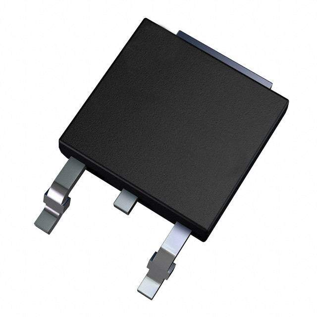
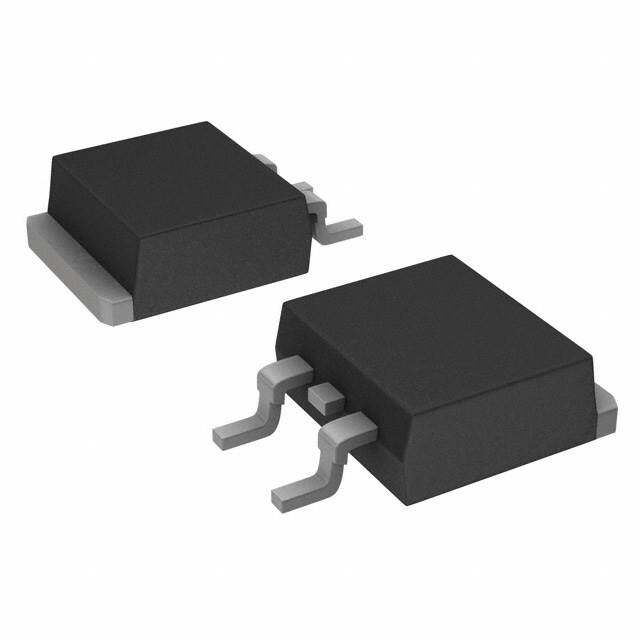
| 产品图片 |
|
| rohs | 符合RoHS无铅 / 符合限制有害物质指令(RoHS)规范要求 |
| 产品系列 | 晶体管,MOSFET,STMicroelectronics STD150N3LLH6DeepGATE™, STripFET™ VI |
| 数据手册 | |
| 产品型号 | STD150N3LLH6 |
| Pd-PowerDissipation | 110 W |
| Pd-功率耗散 | 110 W |
| RdsOn-Drain-SourceResistance | 2.8 mOhms |
| RdsOn-漏源导通电阻 | 2.8 mOhms |
| Vds-Drain-SourceBreakdownVoltage | 30 V |
| Vds-漏源极击穿电压 | 30 V |
| Vgs-Gate-SourceBreakdownVoltage | +/- 20 V |
| Vgs-栅源极击穿电压 | 20 V |
| 上升时间 | 18 ns |
| 下降时间 | 46 ns |
| 不同Id时的Vgs(th)(最大值) | 2.5V @ 250µA |
| 不同Vds时的输入电容(Ciss) | 3700pF @ 25V |
| 不同Vgs时的栅极电荷(Qg) | 29nC @ 4.5V |
| 不同 Id、Vgs时的 RdsOn(最大值) | 2.8 毫欧 @ 40A,10V |
| 产品目录页面 | |
| 产品种类 | MOSFET |
| 供应商器件封装 | D-Pak |
| 其它名称 | 497-8889-6 |
| 其它有关文件 | http://www.st.com/web/catalog/sense_power/FM100/CL824/SC1164/PF219674?referrer=70071840 |
| 典型关闭延迟时间 | 75 ns |
| 功率-最大值 | 110W |
| 包装 | Digi-Reel® |
| 商标 | STMicroelectronics |
| 安装类型 | 表面贴装 |
| 安装风格 | SMD/SMT |
| 封装 | Reel |
| 封装/外壳 | TO-252-3,DPak(2 引线+接片),SC-63 |
| 封装/箱体 | DPAK-2 |
| 工厂包装数量 | 2500 |
| 晶体管极性 | N-Channel |
| 最大工作温度 | + 175 C |
| 最小工作温度 | - 55 C |
| 标准包装 | 1 |
| 漏源极电压(Vdss) | 30V |
| 电流-连续漏极(Id)(25°C时) | 80A (Tc) |
| 系列 | STD150N3LLH6 |
| 通道模式 | Enhancement |
| 配置 | Single |


- 商务部:美国ITC正式对集成电路等产品启动337调查
- 曝三星4nm工艺存在良率问题 高通将骁龙8 Gen1或转产台积电
- 太阳诱电将投资9.5亿元在常州建新厂生产MLCC 预计2023年完工
- 英特尔发布欧洲新工厂建设计划 深化IDM 2.0 战略
- 台积电先进制程称霸业界 有大客户加持明年业绩稳了
- 达到5530亿美元!SIA预计今年全球半导体销售额将创下新高
- 英特尔拟将自动驾驶子公司Mobileye上市 估值或超500亿美元
- 三星加码芯片和SET,合并消费电子和移动部门,撤换高东真等 CEO
- 三星电子宣布重大人事变动 还合并消费电子和移动部门
- 海关总署:前11个月进口集成电路产品价值2.52万亿元 增长14.8%


PDF Datasheet 数据手册内容提取
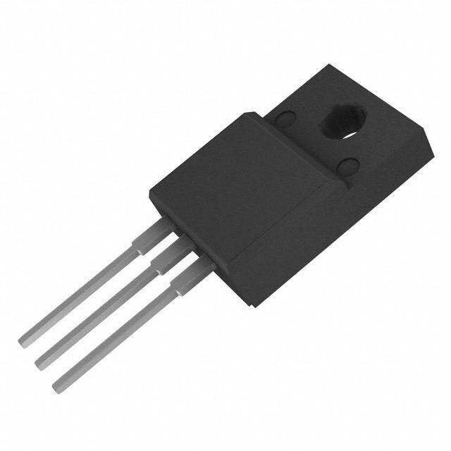
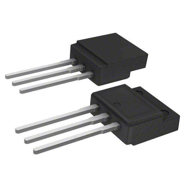
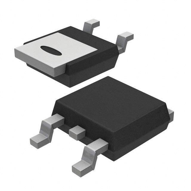
STD150N3LLH6 STP150N3LLH6, STU150N3LLH6 N-channel 30 V, 0.0024 Ω , 80 A, DPAK, IPAK, TO-220 STripFET™ VI DeepGATE™ Power MOSFET Features Type V R max I DSS DS(on) D STD150N3LLH6 30 V 0.0028 Ω 80 A 3 3 STP150N3LLH6 30 V 0.0033 Ω 80 A 2 1 1 STu150N3LLH6 30 V 0.0033 Ω 80 A DPAK IPAK ■ R * Q industry benchmark DS(on) g ■ Extremely low on-resistance R DS(on) 3 ■ High avalanche ruggedness 2 1 TO-220 ■ Low gate drive power losses Application ■ Switching applications Figure 1. Internal schematic diagram Description (cid:36)(cid:0)(cid:8)(cid:52)(cid:33)(cid:34)(cid:0)(cid:79)(cid:82)(cid:0)(cid:18)(cid:9) This product utilizes the 6th generation of design rules of ST’s proprietary STripFET™ technology, with a new gate structure.The resulting Power MOSFET exhibits the lowest R in all DS(on) packages. (cid:39)(cid:8)(cid:17)(cid:9) (cid:51)(cid:8)(cid:19)(cid:9) (cid:33)(cid:45)(cid:16)(cid:17)(cid:20)(cid:23)(cid:20)(cid:86)(cid:17) Table 1. Device summary Order codes Marking Package Packaging STD150N3LLH6 150N3LLH6 DPAK Tape and reel STP150N3LLH6 150N3LLH6 TO-220 Tube STU150N3LLH6 150N3LLH6 IPAK Tube September 2009 Doc ID 15227 Rev 3 1/16 www.st.com 16
Contents STD150N3LLH6, STP150N3LLH6, STU150N3LLH6 Contents 1 Electrical ratings . . . . . . . . . . . . . . . . . . . . . . . . . . . . . . . . . . . . . . . . . . . . 3 2 Electrical characteristics . . . . . . . . . . . . . . . . . . . . . . . . . . . . . . . . . . . . . 4 2.1 Electrical characteristics (curves) . . . . . . . . . . . . . . . . . . . . . . . . . 6 3 Test circuit . . . . . . . . . . . . . . . . . . . . . . . . . . . . . . . . . . . . . . . . . . . . . . . 8 4 Package mechanical data . . . . . . . . . . . . . . . . . . . . . . . . . . . . . . . . . . . . 10 5 Packaging mechanical data . . . . . . . . . . . . . . . . . . . . . . . . . . . . . . . . . . 14 6 Revision history . . . . . . . . . . . . . . . . . . . . . . . . . . . . . . . . . . . . . . . . . . . 15 2/16 Doc ID 15227 Rev 3
STD150N3LLH6, STP150N3LLH6, STU150N3LLH6 Electrical ratings 1 Electrical ratings Table 2. Absolute maximum ratings Symbol Parameter Value Unit VDS Drain-source voltage (VGS = 0) 30 V VGS Gate-source voltage ± 20 V ID (1) Drain current (continuous) at TC = 25 °C 80 A ID Drain current (continuous) at TC = 100 °C 80 A I (2) Drain current (pulsed) 320 A DM PTOT Total dissipation at TC = 25 °C 110 W Derating factor 0.73 W/°C E (3) Single pulse avalanche energy 525 mJ AS Tstg Storage temperature -55 to 175 °C Tj Max. operating junction temperature 175 °C 1. Limited by wire bonding 2. Pulse width limited by safe operating area 3. Starting Tj = 25°C, I = 40 A, V = 25 V D DD Table 3. Thermal resistance Symbol Parameter Value Unit Rthj-case Thermal resistance junction-case max 1.36 °C/W Rthj-amb Thermal resistance junction-case max 100 °C/W Tj Maximum lead temperature for soldering purpose 275 °C Doc ID 15227 Rev 3 3/16
Electrical characteristics STD150N3LLH6, STP150N3LLH6, STU150N3LLH6 2 Electrical characteristics (T = 25 °C unless otherwise specified) CASE Table 4. Static Symbol Parameter Test conditions Min. Typ. Max. Unit Drain-source breakdown V(BR)DSS Voltage ID = 250 µA, VGS= 0 30 V Zero gate voltage drain VDS = 30 V 1 µA I DSS current (VGS = 0) VDS = 30 V,Tc = 125 °C 10 µA Gate body leakage current IGSS (V = 0) VGS = ± 20 V ±100 nA DS VGS(th) Gate threshold voltage VDS = VGS, ID = 250 µA 1 2.5 V V = 10 V, I = 40 A GS D 0.0024 0.0028 Ω SMD version Static drain-source on VGS = 10 V, ID = 40 A 0.0029 0.0033 Ω R DS(on) resistance V = 4.5 V, I = 40 A GS D 0.0034 0.0045 Ω SMD version VGS = 4.5 V, ID = 40 A 0.0039 0.0049 Ω Table 5. Dynamic Symbol Parameter Test conditions Min Typ. Max. Unit Input capacitance Ciss 4040 pF Output capacitance VDS = 25 V, f=1 MHz, Coss - 740 - pF C Reverse transfer VGS = 0 425 pF rss capacitance Qg Total gate charge VDD = 15 V, ID = 80 A 40 nC Qgs Gate-source charge VGS = 4.5 V - 16.3 - nC Qgd Gate-drain charge (see Figure 14) 15.8 nC f = 1 MHz gate bias Bias = 0 test signal RG Gate input resistance - 1.4 - Ω level = 20 mV open drain 4/16 Doc ID 15227 Rev 3
STD150N3LLH6, STP150N3LLH6, STU150N3LLH6 Electrical characteristics Table 6. Switching on/off (inductive load) Symbol Parameter Test conditions Min. Typ. Max. Unit V = 15 V, I = 40 A, td(on) Turn-on delay time DD D 17 ns R = 4.7 Ω, V = 10 V - - t Rise time G GS 18 ns r (see Figure 15) V = 15 V, I = 40 A, td(off) Turn-off delay time DD D 75 ns R = 4.7 Ω, V = 10 V - - t Fall time G GS 46 ns f (see Figure 15) Table 7. Source drain diode Symbol Parameter Test conditions Min. Typ. Max. Unit ISD Source-drain current 80 A - I (1) Source-drain current (pulsed) 320 A SDM VSD(2) Forward on voltage ISD = 40 A, VGS = 0 - 1.1 V I = 80 A, trr Reverse recovery time SD 34 ns di/dt = 100 A/µs, Qrr Reverse recovery charge - 35 nC V = 24 V I Reverse recovery current DD 2.1 A RRM (see Figure 17) 1. Pulse width limited by safe operating area 2. Pulsed: pulse duration = 300 µs, duty cycle 1.5% Doc ID 15227 Rev 3 5/16
Electrical characteristics STD150N3LLH6, STP150N3LLH6, STU150N3LLH6 2.1 Electrical characteristics (curves) Figure 2. Safe operating area Figure 3. Thermal impedance ID AM03997v1 1(0A0) OpLeirmaittieodn ibny thmisa x arReDa Si(son) 10 100µs 1ms Tj=150°C 10ms 1 Tc=25°C Sinlge pulse 0.1 0.1 1 10 VDS(V) Figure 4. Output characteristics Figure 5. Transfer characteristics AM03998v1 AM03999v1 ID ID (A) (A) VGS=10V 350 300 VDS=1V 300 250 5V 250 4V 200 200 150 150 100 100 3V 50 50 0 0 0 2 4 VDS(V) 0 2 4 6 8 10 VGS(V) Figure 6. Normalized BV vs temperature Figure 7. Static drain-source on resistance DSS BVDSS AM04903v1 RDS(on) AM04905v1 (Ω) (norm) 1.06 4.5 VGS=10V ID=250µA 4.0 1.04 3.5 3.0 1.02 2.5 1.00 2.0 0.98 1.5 1.0 0.96 0.5 0.94 0.0 -50 0 50 100 150 TJ(°C) 0 20 40 60 80 ID(A) 6/16 Doc ID 15227 Rev 3
STD150N3LLH6, STP150N3LLH6, STU150N3LLH6 Electrical characteristics Figure 8. Gate charge vs gate-source voltage Figure 9. Capacitance variations VGS AM04000v1 C AM00893v1 (V) (pF) VDD=15V f=1MHz 12 ID=80A 6100 10 4600 8 Ciss 6 3100 4 1600 2 Coss Crss 0 100 0 20 40 60 80 100 Qg(nC) 0 5 10 15 20 25 VDS(V) Figure 10. Normalized gate threshold voltage Figure 11. Normalized on resistance vs vs temperature temperature VGS(th) AM04901v1 RDS(on) AM04902v1 (norm) (norm) ID=250µA 1.6 ID=40A 1.1 VGS=10V 1.4 1.0 1.2 0.8 1.0 0.8 0.6 0.6 0.4 0.4 0.2 0.2 0 -50 0 50 100 150 TJ(°C) -50 -25 0 25 50 75 100 TJ(°C) Figure 12. Source-drain diode forward characteristics VSD AM04906v1 (V) TJ=-50°C 1.0 0.9 0.8 0.7 TJ=25°C TJ=175°C 0.6 0.5 0.4 0 20 40 60 80 ISD(A) Doc ID 15227 Rev 3 7/16
Test circuit STD150N3LLH6, STP150N3LLH6, STU150N3LLH6 3 Test circuit Figure 13. Switching times test circuit for Figure 14. Gate charge test circuit resistive load VDD 12V 47kΩ 1kΩ 100nF RL 2µ20F0 3µ.F3 VDD IG=CONST VD Vi=20V=VGMAX 100Ω D.U.T. VGS 2200 RG D.U.T. µF 2.7kΩ VG PW 47kΩ 1kΩ PW AM01468v1 AM01469v1 Figure 15. Test circuit for inductive load Figure 16. Unclamped Inductive load test switching and diode recovery times circuit L A A A D FAST L=100µH VD G D.U.T. DIODE 2200 3.3 µF µF VDD S B 3.3 1000 B B µF µF 25Ω D VDD ID G RG S Vi D.U.T. Pw AM01470v1 AM01471v1 Figure 17. Unclamped inductive waveform Figure 18. Switching time waveform V(BR)DSS ton toff VD tdon tr tdoff tf 90% 90% IDM 10% ID 0 10% VDS VDD VDD VGS 90% AM01472v1 0 10% AM01473v1 8/16 Doc ID 15227 Rev 3
STD150N3LLH6, STP150N3LLH6, STU150N3LLH6 Test circuit Figure 19. Gate charge waveform Id Vds Vgs Vgs(th) Qgs1 Qgs2 Qgd Doc ID 15227 Rev 3 9/16
Package mechanical data STD150N3LLH6, STP150N3LLH6, STU150N3LLH6 4 Package mechanical data In order to meet environmental requirements, ST offers these devices in different grades of ECOPACK® packages, depending on their level of environmental compliance. ECOPACK® specifications, grade definitions and product status are available at: www.st.com. ECOPACK is an ST trademark. 10/16 Doc ID 15227 Rev 3
STD150N3LLH6, STP150N3LLH6, STU150N3LLH6 Package mechanical data TO-251 (IPAK) mechanical data mm. DIM. min. typ max. A 2.20 2.40 A1 0.90 1.10 b 0.64 0.90 b2 0.95 b4 5.20 5.40 c 0.45 0.60 c2 0.48 0.60 D 6.00 6.20 E 6.40 6.60 e 2.28 e1 4.40 4.60 H 16.10 L 9.00 9.40 (L1) 0.80 1.20 L2 0.80 V1 10 o 0068771_H Doc ID 15227 Rev 3 11/16
Package mechanical data STD150N3LLH6, STP150N3LLH6, STU150N3LLH6 TO-252 (DPAK) mechanical data mm. DIM. min. typ max. A 2.20 2.40 A1 0.90 1.10 A2 0.03 0.23 b 0.64 0.90 b4 5.20 5.40 c 0.45 0.60 c2 0.48 0.60 D 6.00 6.20 D1 5.10 E 6.40 6.60 E1 4.70 e 2.28 e1 4.40 4.60 H 9.35 10.10 L 1 L1 2.80 L2 0.80 L4 0.60 1 R 0.20 V2 0 o 8o 0068772_G 12/16 Doc ID 15227 Rev 3
STD150N3LLH6, STP150N3LLH6, STU150N3LLH6 Package mechanical data TO-220 mechanical data mm inch Dim Min Typ Max Min Typ Max A 4.40 4.60 0.173 0.181 b 0.61 0.88 0.024 0.034 b1 1.14 1.70 0.044 0.066 c 0.48 0.70 0.019 0.027 D 15.25 15.75 0.6 0.62 D1 1.27 0.050 E 10 10.40 0.393 0.409 e 2.40 2.70 0.094 0.106 e1 4.95 5.15 0.194 0.202 F 1.23 1.32 0.048 0.051 H1 6.20 6.60 0.244 0.256 J1 2.40 2.72 0.094 0.107 L 13 14 0.511 0.551 L1 3.50 3.93 0.137 0.154 L20 16.40 0.645 L30 28.90 1.137 ∅P 3.75 3.85 0.147 0.151 Q 2.65 2.95 0.104 0.116 Doc ID 15227 Rev 3 13/16
Packaging mechanical data STD150N3LLH6, STP150N3LLH6, STU150N3LLH6 5 Packaging mechanical data DPAK FOOTPRINT All dimensions are in millimeters TAPE AND REEL SHIPMENT REEL MECHANICAL DATA mm inch DIM. MIN. MAX. MIN. MAX. A 330 12.992 B 1.5 0.059 C 12.8 13.2 0.504 0.520 D 20.2 0.795 G 16.4 18.4 0.645 0.724 N 50 1.968 T 22.4 0.881 BASE QTY BULK QTY TAPE MECHANICAL DATA 2500 2500 mm inch DIM. MIN. MAX. MIN. MAX. A0 6.8 7 0.267 0.275 B0 10.4 10.6 0.409 0.417 B1 12.1 0.476 D 1.5 1.6 0.059 0.063 D1 1.5 0.059 E 1.65 1.85 0.065 0.073 F 7.4 7.6 0.291 0.299 K0 2.55 2.75 0.100 0.108 P0 3.9 4.1 0.153 0.161 P1 7.9 8.1 0.311 0.319 P2 1.9 2.1 0.075 0.082 R 40 1.574 W 15.7 16.3 0.618 0.641 14/16 Doc ID 15227 Rev 3
STD150N3LLH6, STP150N3LLH6, STU150N3LLH6 Revision history 6 Revision history T able 8. Document revision history Date Revision Changes 01-Dec-2008 1 First release – Document status promoted from preliminary data to datasheet 20-Jul-2009 2 – Added new package, mechanical data: TO-220 10-Sep-2009 3 Q and Q values have been modified on Table5: Dynamic gs gd Doc ID 15227 Rev 3 15/16
STD150N3LLH6, STP150N3LLH6, STU150N3LLH6 Please Read Carefully: Information in this document is provided solely in connection with ST products. STMicroelectronics NV and its subsidiaries (“ST”) reserve the right to make changes, corrections, modifications or improvements, to this document, and the products and services described herein at any time, without notice. All ST products are sold pursuant to ST’s terms and conditions of sale. Purchasers are solely responsible for the choice, selection and use of the ST products and services described herein, and ST assumes no liability whatsoever relating to the choice, selection or use of the ST products and services described herein. No license, express or implied, by estoppel or otherwise, to any intellectual property rights is granted under this document. If any part of this document refers to any third party products or services it shall not be deemed a license grant by ST for the use of such third party products or services, or any intellectual property contained therein or considered as a warranty covering the use in any manner whatsoever of such third party products or services or any intellectual property contained therein. UNLESS OTHERWISE SET FORTH IN ST’S TERMS AND CONDITIONS OF SALE ST DISCLAIMS ANY EXPRESS OR IMPLIED WARRANTY WITH RESPECT TO THE USE AND/OR SALE OF ST PRODUCTS INCLUDING WITHOUT LIMITATION IMPLIED WARRANTIES OF MERCHANTABILITY, FITNESS FOR A PARTICULAR PURPOSE (AND THEIR EQUIVALENTS UNDER THE LAWS OF ANY JURISDICTION), OR INFRINGEMENT OF ANY PATENT, COPYRIGHT OR OTHER INTELLECTUAL PROPERTY RIGHT. UNLESS EXPRESSLY APPROVED IN WRITING BY AN AUTHORIZED ST REPRESENTATIVE, ST PRODUCTS ARE NOT RECOMMENDED, AUTHORIZED OR WARRANTED FOR USE IN MILITARY, AIR CRAFT, SPACE, LIFE SAVING, OR LIFE SUSTAINING APPLICATIONS, NOR IN PRODUCTS OR SYSTEMS WHERE FAILURE OR MALFUNCTION MAY RESULT IN PERSONAL INJURY, DEATH, OR SEVERE PROPERTY OR ENVIRONMENTAL DAMAGE. ST PRODUCTS WHICH ARE NOT SPECIFIED AS "AUTOMOTIVE GRADE" MAY ONLY BE USED IN AUTOMOTIVE APPLICATIONS AT USER’S OWN RISK. Resale of ST products with provisions different from the statements and/or technical features set forth in this document shall immediately void any warranty granted by ST for the ST product or service described herein and shall not create or extend in any manner whatsoever, any liability of ST. ST and the ST logo are trademarks or registered trademarks of ST in various countries. Information in this document supersedes and replaces all information previously supplied. The ST logo is a registered trademark of STMicroelectronics. All other names are the property of their respective owners. © 2009 STMicroelectronics - All rights reserved STMicroelectronics group of companies Australia - Belgium - Brazil - Canada - China - Czech Republic - Finland - France - Germany - Hong Kong - India - Israel - Italy - Japan - Malaysia - Malta - Morocco - Philippines - Singapore - Spain - Sweden - Switzerland - United Kingdom - United States of America www.st.com 16/16 Doc ID 15227 Rev 3
Mouser Electronics Authorized Distributor Click to View Pricing, Inventory, Delivery & Lifecycle Information: S TMicroelectronics: STD150N3LLH6 STU150N3LLH6 STP150N3LLH6