ICGOO在线商城 > 分立半导体产品 > 晶体管 - FET,MOSFET - 单 > STB20N95K5
 Datasheet下载
- 型号: STB20N95K5
- 制造商: STMicroelectronics
- 库位|库存: xxxx|xxxx
- 要求:
| 数量阶梯 | 香港交货 | 国内含税 |
| +xxxx | $xxxx | ¥xxxx |
查看当月历史价格
查看今年历史价格
STB20N95K5产品简介:
ICGOO电子元器件商城为您提供STB20N95K5由STMicroelectronics设计生产,在icgoo商城现货销售,并且可以通过原厂、代理商等渠道进行代购。 STB20N95K5价格参考。STMicroelectronicsSTB20N95K5封装/规格:晶体管 - FET,MOSFET - 单, 表面贴装 N 沟道 950V 17.5A(Tc) 250W(Tc) D2PAK。您可以下载STB20N95K5参考资料、Datasheet数据手册功能说明书,资料中有STB20N95K5 详细功能的应用电路图电压和使用方法及教程。
STMicroelectronics的STB20N95K5是一款单通道MOSFET(金属-氧化物-半导体场效应晶体管),具有多种应用场景,尤其适用于需要高效功率管理的电路设计。以下是其主要应用场景:

 1. 电源管理
STB20N95K5常用于开关电源(SMPS)和直流-直流转换器中,作为功率开关或同步整流器。其低导通电阻(Rds(on))特性有助于减少功率损耗,提高效率,特别适合于笔记本电脑、平板电脑和其他便携式电子设备的电源管理系统。

 2. 电机驱动
该MOSFET可用于驱动小型直流电机或步进电机,特别是在电池供电的设备中。由于其低功耗和高可靠性,STB20N95K5在无人机、电动工具、智能家居设备等应用中表现出色。

 3. 负载切换
在汽车电子系统中,STB20N95K5可以用作负载开关,控制不同电路模块的供电状态。例如,在车身控制系统中,它可以用于管理车灯、雨刷、空调等设备的电源通断,确保系统的稳定性和安全性。

 4. 保护电路
STB20N95K5还可以用于过流保护和短路保护电路。通过检测电流并快速响应,它可以有效防止电路因过载或短路而损坏,广泛应用于消费电子、工业控制等领域。

 5. 音频放大器
在某些音频放大器设计中,STB20N95K5可以用作输出级的功率开关,帮助实现高效的音频信号放大。其低噪声特性和稳定的性能使其成为高品质音频设备的理想选择。

 6. 太阳能逆变器
在太阳能发电系统中,STB20N95K5可以用于逆变器中的功率转换部分,将直流电转换为交流电。其高效能和耐用性使得它在可再生能源领域有广泛应用。

 总结
STB20N95K5凭借其出色的电气特性,如低导通电阻、高击穿电压和良好的热稳定性,广泛应用于电源管理、电机驱动、负载切换、保护电路、音频放大器以及太阳能逆变器等多种场景。它不仅能够提高系统的效率,还能增强系统的可靠性和安全性。
| 参数 | 数值 |
| 产品目录 | |
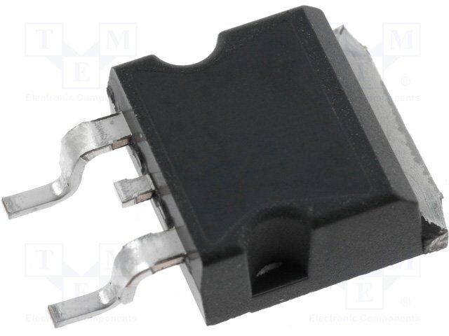
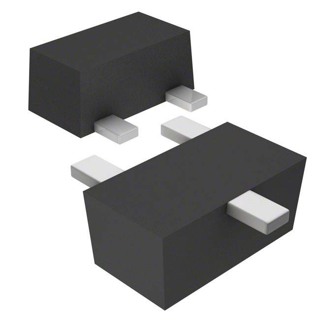
| 描述 | MOSFET N-CH 950V 17.5A D2PAKMOSFET N-Ch 950V 0.275 Ohm 17.5A SuperMESH 5 |
| 产品分类 | FET - 单分离式半导体 |
| FET功能 | 标准 |
| FET类型 | MOSFET N 通道,金属氧化物 |
| Id-ContinuousDrainCurrent | 17.5 A |
| Id-连续漏极电流 | 17.5 A |
| 品牌 | STMicroelectronics |
| 产品手册 | |
| 产品图片 |
|
| rohs | 符合RoHS无铅 / 符合限制有害物质指令(RoHS)规范要求 |
| 产品系列 | 晶体管,MOSFET,STMicroelectronics STB20N95K5SuperMESH5™ |
| 数据手册 | |
| 产品型号 | STB20N95K5 |
| Pd-PowerDissipation | 250 W |
| Pd-功率耗散 | 250 W |
| Qg-GateCharge | 40 nC |
| Qg-栅极电荷 | 40 nC |
| RdsOn-Drain-SourceResistance | 330 mOhms |
| RdsOn-漏源导通电阻 | 330 mOhms |
| Vds-Drain-SourceBreakdownVoltage | 950 V |
| Vds-漏源极击穿电压 | 950 V |
| Vgs-Gate-SourceBreakdownVoltage | 30 V |
| Vgs-栅源极击穿电压 | 30 V |
| 不同Id时的Vgs(th)(最大值) | 5V @ 100µA |
| 不同Vds时的输入电容(Ciss) | 1500pF @ 100V |
| 不同Vgs时的栅极电荷(Qg) | 40nC @ 10V |
| 不同 Id、Vgs时的 RdsOn(最大值) | 330 毫欧 @ 9A,10V |
| 产品种类 | MOSFET |
| 供应商器件封装 | D2PAK |
| 其它名称 | 497-12850-6 |
| 其它有关文件 | http://www.st.com/web/catalog/sense_power/FM100/CL824/SC1168/PF252559?referrer=70071840 |
| 功率-最大值 | 250W |
| 包装 | Digi-Reel® |
| 商标 | STMicroelectronics |
| 安装类型 | 表面贴装 |
| 安装风格 | SMD/SMT |
| 封装 | Reel |
| 封装/外壳 | TO-263-3,D²Pak(2 引线+接片),TO-263AB |
| 封装/箱体 | D2PAK-2 |
| 工厂包装数量 | 1000 |
| 晶体管极性 | N-Channel |
| 最大工作温度 | + 150 C |
| 最小工作温度 | - 55 C |
| 标准包装 | 1 |
| 漏源极电压(Vdss) | 950V |
| 电流-连续漏极(Id)(25°C时) | 17.5A (Tc) |
| 系列 | STB20N95K5 |


- 商务部:美国ITC正式对集成电路等产品启动337调查
- 曝三星4nm工艺存在良率问题 高通将骁龙8 Gen1或转产台积电
- 太阳诱电将投资9.5亿元在常州建新厂生产MLCC 预计2023年完工
- 英特尔发布欧洲新工厂建设计划 深化IDM 2.0 战略
- 台积电先进制程称霸业界 有大客户加持明年业绩稳了
- 达到5530亿美元!SIA预计今年全球半导体销售额将创下新高
- 英特尔拟将自动驾驶子公司Mobileye上市 估值或超500亿美元
- 三星加码芯片和SET,合并消费电子和移动部门,撤换高东真等 CEO
- 三星电子宣布重大人事变动 还合并消费电子和移动部门
- 海关总署:前11个月进口集成电路产品价值2.52万亿元 增长14.8%


PDF Datasheet 数据手册内容提取
STB20N95K5, STF20N95K5, STP20N95K5, STW20N95K5 N-channel 950 V, 0.275 Ω typ., 17.5 A MDmesh™ K5 Power MOSFETs in D²PAK, TO-220FP, TO-220 and TO-247 Datasheet p- parocdukcatiogn deasta Features Order code VDS RDS(on) max. ID PTOT STB20N95K5 250 W STF20N95K5 40 W 950 V 0.330 Ω 17.5 A STP20N95K5 250 W STW20N95K5 Industry’s lowest R x area DS(on) Industry’s best FoM (figure of merit) Ultra-low gate charge Figure 1: Internal schematic diagram 100% avalanche tested Zener-protected Applications Switching applications Description These very high voltage N-channel Power MOSFETs are designed using MDmesh™ K5 technology based on an innovative proprietary vertical structure. The result is a dramatic reduction in on-resistance and ultra-low gate charge for applications requiring superior power density and high efficiency. Table 1: Device summary Order code Marking Package Packing STB20N95K5 D²PAK Tape and reel STF20N95K5 TO-220FP 20N95K5 STP20N95K5 TO-220 Tube STW20N95K5 TO-247 January 2017 DocID16825 Rev 5 1/22 This is information on a product in full production. www.st.com
Contents STB20N95K5, STF20N95K5, STP20N95K5, STW20N95K5 Contents 1 Electrical ratings ............................................................................. 3 2 Electrical characteristics ................................................................ 4 2.1 Electrical characteristics (curves) ...................................................... 6 3 Test circuits ..................................................................................... 9 4 Package information ..................................................................... 10 4.1 D2PAK package information ............................................................ 10 4.2 TO-220FP package information ...................................................... 13 4.3 TO-220 type A package information ................................................ 15 4.4 TO-247 package information ........................................................... 17 4.5 D2PAK packing information ............................................................. 19 5 Revision history ............................................................................ 21 2/22 DocID16825 Rev 5
STB20N95K5, STF20N95K5, STP20N95K5, Electrical ratings STW20N95K5 1 Electrical ratings Table 2: Absolute maximum ratings Value D²PAK Symbol Parameter Unit TO-220 TO-220FP TO-247 VGS Gate-source voltage ±30 V ID Drain current (continuous) at TC = 25 °C 17.5 A ID Drain current (continuous) at TC = 100 °C 11 A ID(1) Drain current (pulsed) 70 A PTOT Total dissipation at TC = 25 °C 250 40 W Gate-source human body model (R= 1,5 kΩ, ESD 2 kV C = 100 pF) Insulation withstand voltage (RMS) from all VISO three leads to external heat sink (t = 1 s; 2500 V TC = 25 °C) dv/dt (2) Peak diode recovery voltage slope 6 V/ns dv/dt (3) MOSFET dv/dt ruggedness 50 Tj Operating junction temperature range -55 to 150 °C Tstg Storage temperature range Notes: (1)Pulse width limited by safe operating area. (2)ISD ≤ 17.5 A, di/dt ≤ 100 A/μs; VDS peak ≤ V(BR)DSS (3)VDS ≤ 760 V Table 3: Thermal data Value Symbol Parameter Unit D²PAK TO-220 TO-247 TO-220FP Rthj-case Thermal resistance junction-case 0.5 3.1 Rthj-amb Thermal resistance junction-ambient 62.5 50 62.5 °C/W Rthj-pcb(1) Thermal resistance junction-pcb 30 Notes: (1) When mounted on 1 inch² FR-4 board, 2 Oz Cu. Table 4: Avalanche characteristics Symbol Parameter Value Unit IAR Avalanche current, repetitive or not repetitive (pulse width limited by Tjmax.) 6 A EAS Single pulse avalanche energy (starting Tj = 25 °C, ID = IAR, VDD = 50 V) 200 mJ DocID16825 Rev 5 3/22
Electrical characteristics STB20N95K5, STF20N95K5, STP20N95K5, STW20N95K5 2 Electrical characteristics T = 25 °C unless otherwise specified C Table 5: On/off-state Symbol Parameter Test conditions Min. Typ. Max. Unit V(BR)DSS Drain-source breakdown voltage VGS = 0 V, ID = 1 mA 950 V VGS = 0 V, VDS = 950 V 1 µA IDSS Zero-gate voltage drain current VGS = 0 V, VDS = 950 V 50 µA TC = 125 °C(1) IGSS Gate body leakage current VDS = 0 V, VGS = ±20 V ±10 µA VGS(th) Gate threshold voltage VDS = VGS, ID = 100 µA 3 4 5 V RDS(on) Static drain-source on-resistance VGS = 10 V, ID = 9 A 0.275 0.330 Ω Notes: (1)Defined by design, not subject to production test. Table 6: Dynamic Symbol Parameter Test conditions Min. Typ. Max. Unit Ciss Input capacitance - 1550 - pF Coss Output capacitance VVDGSS == 100 V0 V, f = 1 MHz, - 140 - pF Crss Reverse transfer capacitance - 1 - pF Equivalent capacitance energy Co(er)(1) related VGS = 0 V, VDS = 0 to - 65 - pF Equivalent capacitance time 760 V Co(tr)(2) related 178 - pF Rg Intrinsic gate resistance f = 1 MHz , ID = 0 A - 3.5 - Ω Qg Total gate charge VDD = 760 V, - 48 - nC Qgs Gate-source charge ID = 17.5 A - 9 - nC VGS= 10 V (see Figure 20: "Test Qgd Gate-drain charge circuit for gate charge - 32.5 - nC behavior") Notes: (1)Co(er) is a constant capacitance value that gives the same stored energy as Coss while VDS is rising from 0 to 80% VDSS. (2)Co(tr) is a constant capacitance value that gives the same charging time as Coss while VDS is rising from 0 to 80% VDSS. 4/22 DocID16825 Rev 5
STB20N95K5, STF20N95K5, STP20N95K5, Electrical characteristics STW20N95K5 Table 7: Switching times Symbol Parameter Test conditions Min. Typ. Max. Unit Turn-on td(on) delay time VDD= 475 V, ID = 9 A, RG = 4.7 Ω - 18 - ns tr Rise time VGS = 10 V - 9 - ns (see Figure 19: "Test circuit for resistive Turn-off td(off) delay time load switching times" and Figure 24: - 65 - ns "Switching time waveform") tf Fall time - 18 - ns Table 8: Source-drain diode Symbol Parameter Test conditions Min. Typ. Max. Unit Source-drain ISD current - 17.5 A Source-drain ISDM(1) current (pulsed) - 70 A Forward on VSD(2) voltage ISD = 17.5 A, VGS = 0 V - 1.5 V Reverse recovery trr time ISD = 17.5 A, di/dt = 100 A/µs, - 513 ns Reverse recovery VDD = 60 V Qrr charge (see Figure 21: "Test circuit for - 12 µC inductive load switching and diode IRRM Rcuervreenrst e recovery recovery times") - 46 A Reverse recovery trr time ISD = 17.5 A, di/dt = 100 A/µs - 670 ns Reverse recovery VDD = 60 V, Tj = 150 °C Qrr charge (see Figure 21: "Test circuit for - 15 µC inductive load switching and diode Reverse recovery recovery times") IRRM current - 44 A Notes: (1)Pulse width limited by safe operating area (2)Pulsed: pulse duration = 300 µs, duty cycle 1.5% Table 9: Gate-source Zener diode Symbol Parameter Test conditions Min. Typ. Max. Unit V(BR) GSO Gate-source breakdown voltage IGS = ± 1 mA, ID = 0 A 30 - - V The built-in back-to-back Zener diodes are specifically designed to enhance the ESD performance of the device. The Zener voltage facilitates efficient and cost-effective device integrity protection, thus eliminating the need for additional external componentry. DocID16825 Rev 5 5/22
Electrical characteristics STB20N95K5, STF20N95K5, STP20N95K5, STW20N95K5 2.1 Electrical characteristics (curves) Figure 3: Thermal impedance for D²PAK and Figure 2: Safe operating area for D²PAK and TO-220 TO-220 Figure 4: Safe operating area for TO-220FP Figure 5: Thermal impedance for TO-220FP Figure 6: Safe operating area for TO-247 Figure 7: Thermal impedance for TO-247 6/22 DocID16825 Rev 5
STB20N95K5, STF20N95K5, STP20N95K5, Electrical characteristics STW20N95K5 Figure 8: Output characteristics Figure 9: Transfer characteristics Figure 10: Gate charge vs gate-source voltage Figure 11: Static drain-source on-resistance Figure 12: Capacitance variation Figure 13: Output capacitance stored energy DocID16825 Rev 5 7/22
Electrical characteristics STB20N95K5, STF20N95K5, STP20N95K5, STW20N95K5 Figure 14: Normalized gate threshold voltage vs Figure 15: Normalized on-resistance vs temperature temperature Figure 16: Maximum avalanche energy vs. starting TJ Figure 17: Normalized V(BR)DSS vs. temperature Figure 18: Source-drain diode forward characteristics 8/22 DocID16825 Rev 5
STB20N95K5, STF20N95K5, STP20N95K5, Test circuits STW20N95K5 3 Test circuits Figure 19: Test circuit for resistive load Figure 20: Test circuit for gate charge switching times behavior VDD RL I= CONST VGS G 100 Ω D.U.T. pulse width + 2.7 kΩ 2200 VG μF 47 kΩ 1 kΩ AM01469v10 Figure 21: Test circuit for inductive load switching and diode recovery times Figure 22: Unclamped inductive load test circuit Figure 23: Unclamped inductive waveform Figure 24: Switching time waveform DocID16825 Rev 5 9/22
Package information STB20N95K5, STF20N95K5, STP20N95K5, STW20N95K5 4 Package information In order to meet environmental requirements, ST offers these devices in different grades of ECOPACK® packages, depending on their level of environmental compliance. ECOPACK® specifications, grade definitions and product status are available at: www.st.com. ECOPACK® is an ST trademark. 4.1 D2PAK package information Figure 25: D²PAK (TO-263) type A package outline 0079457_A_rev22 10/22 DocID16825 Rev 5
STB20N95K5, STF20N95K5, STP20N95K5, Package information STW20N95K5 Table 10: D²PAK (TO-263) type A package mechanical data mm Dim. Min. Typ. Max. A 4.40 4.60 A1 0.03 0.23 b 0.70 0.93 b2 1.14 1.70 c 0.45 0.60 c2 1.23 1.36 D 8.95 9.35 D1 7.50 7.75 8.00 D2 1.10 1.30 1.50 E 10 10.40 E1 8.50 8.70 8.90 E2 6.85 7.05 7.25 e 2.54 e1 4.88 5.28 H 15 15.85 J1 2.49 2.69 L 2.29 2.79 L1 1.27 1.40 L2 1.30 1.75 R 0.4 V2 0° 8° DocID16825 Rev 5 11/22
Package information STB20N95K5, STF20N95K5, STP20N95K5, STW20N95K5 Figure 26: D²PAK (TO-263) recommended footprint (dimensions are in mm) 12/22 DocID16825 Rev 5
STB20N95K5, STF20N95K5, STP20N95K5, Package information STW20N95K5 4.2 TO-220FP package information Figure 27: TO-220FP package outline DocID16825 Rev 5 13/22
Package information STB20N95K5, STF20N95K5, STP20N95K5, STW20N95K5 Table 11: TO-220FP package mechanical data mm Dim. Min. Typ. Max. A 4.4 4.6 B 2.5 2.7 D 2.5 2.75 E 0.45 0.7 F 0.75 1 F1 1.15 1.70 F2 1.15 1.70 G 4.95 5.2 G1 2.4 2.7 H 10 10.4 L2 16 L3 28.6 30.6 L4 9.8 10.6 L5 2.9 3.6 L6 15.9 16.4 L7 9 9.3 Dia 3 3.2 14/22 DocID16825 Rev 5
STB20N95K5, STF20N95K5, STP20N95K5, Package information STW20N95K5 4.3 TO-220 type A package information Figure 28: TO-220 type A package outline DocID16825 Rev 5 15/22
Package information STB20N95K5, STF20N95K5, STP20N95K5, STW20N95K5 Table 12: TO-220 type A mechanical data mm Dim. Min. Typ. Max. A 4.40 4.60 b 0.61 0.88 b1 1.14 1.55 c 0.48 0.70 D 15.25 15.75 D1 1.27 E 10.00 10.40 e 2.40 2.70 e1 4.95 5.15 F 1.23 1.32 H1 6.20 6.60 J1 2.40 2.72 L 13.00 14.00 L1 3.50 3.93 L20 16.40 L30 28.90 øP 3.75 3.85 Q 2.65 2.95 16/22 DocID16825 Rev 5
STB20N95K5, STF20N95K5, STP20N95K5, Package information STW20N95K5 4.4 TO-247 package information Figure 29: TO-247 package outline 0075325_8 DocID16825 Rev 5 17/22
Package information STB20N95K5, STF20N95K5, STP20N95K5, STW20N95K5 Table 13: TO-247 package mechanical data mm Dim. Min. Typ. Max. A 4.85 5.15 A1 2.20 2.60 b 1.0 1.40 b1 2.0 2.40 b2 3.0 3.40 c 0.40 0.80 D 19.85 20.15 E 15.45 15.75 e 5.30 5.45 5.60 L 14.20 14.80 L1 3.70 4.30 L2 18.50 ØP 3.55 3.65 ØR 4.50 5.50 S 5.30 5.50 5.70 18/22 DocID16825 Rev 5
STB20N95K5, STF20N95K5, STP20N95K5, Package information STW20N95K5 4.5 D2PAK packing information Figure 30: Tape outline DocID16825 Rev 5 19/22
Package information STB20N95K5, STF20N95K5, STP20N95K5, STW20N95K5 Figure 31: Reel outline Table 14: D²PAK tape and reel mechanical data Tape Reel mm mm Dim. Dim. Min. Max. Min. Max. A0 10.5 10.7 A 330 B0 15.7 15.9 B 1.5 D 1.5 1.6 C 12.8 13.2 D1 1.59 1.61 D 20.2 E 1.65 1.85 G 24.4 26.4 F 11.4 11.6 N 100 K0 4.8 5.0 T 30.4 P0 3.9 4.1 P1 11.9 12.1 Base quantity 1000 P2 1.9 2.1 Bulk quantity 1000 R 50 T 0.25 0.35 W 23.7 24.3 20/22 DocID16825 Rev 5
STB20N95K5, STF20N95K5, STP20N95K5, Revision history STW20N95K5 5 Revision history Table 15: Document revision history Date Revision Changes 25-Nov-2009 1 First release. 12-Jan-2010 2 Corrected VGS value in Table 2: Absolute maximum ratings. Inserted device in D2PAK. Document status promoted from preliminary data to datasheet. 22-Dec-2011 3 Added: Section 2.1: Electrical characteristics (curves) Updated Section 4: Package mechanical data. Added Section 5: Packaging mechanical data. Minor text changes. 06-Jun-2012 4 Figure 9: Transfer characteristics has been updated. Updated title, features, description and schematic diagram in cover page. Minor text changes in Section 1: "Electrical ratings" and Section 2: 16-Jan-2017 5 "Electrical characteristics". Updated Section 2.1: "Electrical characteristics (curves)" Updated package information section. DocID16825 Rev 5 21/22
STB20N95K5, STF20N95K5, STP20N95K5, STW20N95K5 IMPORTANT NOTICE – PLEASE READ CAREFULLY STMicroelectronics NV and its subsidiaries (“ST”) reserve the right to make changes, corrections, enhancements, modifications, and improvements to ST products and/or to this document at any time without notice. Purchasers should obtain the latest relevant information on ST products before placing orders. ST products are sold pursuant to ST’s terms and conditions of sale in place at the time of order acknowledgement. Purchasers are solely responsible for the choice, selection, and use of ST products and ST assumes no liability for application assistance or the design of Purchasers’ products. No license, express or implied, to any intellectual property right is granted by ST herein. Resale of ST products with provisions different from the information set forth herein shall void any warranty granted by ST for such product. ST and the ST logo are trademarks of ST. All other product or service names are the property of their respective owners. Information in this document supersedes and replaces information previously supplied in any prior versions of this document. © 2017 STMicroelectronics – All rights reserved 22/22 DocID16825 Rev 5
Mouser Electronics Authorized Distributor Click to View Pricing, Inventory, Delivery & Lifecycle Information: S TMicroelectronics: STF20N95K5 STP20N95K5 STW20N95K5 STB20N95K5