ICGOO在线商城 > 分立半导体产品 > 晶体管 - FET,MOSFET - 单 > FDS3580
 Datasheet下载
- 型号: FDS3580
- 制造商: Fairchild Semiconductor
- 库位|库存: xxxx|xxxx
- 要求:
| 数量阶梯 | 香港交货 | 国内含税 |
| +xxxx | $xxxx | ¥xxxx |
查看当月历史价格
查看今年历史价格
FDS3580产品简介:
ICGOO电子元器件商城为您提供FDS3580由Fairchild Semiconductor设计生产,在icgoo商城现货销售,并且可以通过原厂、代理商等渠道进行代购。 FDS3580价格参考。Fairchild SemiconductorFDS3580封装/规格:晶体管 - FET,MOSFET - 单, 表面贴装 N 沟道 80V 7.6A(Ta) 2.5W(Ta) 8-SOIC。您可以下载FDS3580参考资料、Datasheet数据手册功能说明书,资料中有FDS3580 详细功能的应用电路图电压和使用方法及教程。
ON Semiconductor(安森美半导体)的FDS3580是一款N沟道增强型MOSFET晶体管,广泛应用于各种电力电子场景。以下是其主要应用场景:

1. 开关电源(SMPS)
   FDS3580适用于开关电源中的高频开关应用,例如降压、升压或反激式转换器。其低导通电阻(Rds(on))和快速开关特性有助于提高效率并减少能量损耗。

2. 电机驱动
   该MOSFET可用于小型直流电机驱动电路中,作为功率开关控制电机的启动、停止和速度调节。其高电流处理能力和耐热性能确保了稳定运行。

3. 负载开关
   在便携式设备或嵌入式系统中,FDS3580可用作负载开关以实现电源管理。它能够快速响应负载变化,并提供低功耗的操作模式。

4. 电池管理
   该器件适合用于锂电池保护电路,监控充电/放电过程中的电流和电压。通过精确控制开关状态,可以防止过充或过放现象发生。

5. 逆变器与DC-DC转换器
   FDS3580在逆变器和DC-DC转换模块中有广泛应用,尤其是在需要高效能转换和小体积设计的情况下。其优化的栅极电荷和开关速度使其成为理想选择。

6. LED驱动器
   用于恒流源驱动大功率LED时,此MOSFET可保证输出电流的稳定性,同时降低发热影响。

7. 通信设备
   在基站、路由器等通信设施中,FDS3580可作为信号调理和功率分配的关键元件。

总结来说,FDS3580凭借其优异的电气特性和可靠性,在消费电子、工业自动化、汽车电子以及通信领域都有广泛的用途。
| 参数 | 数值 |
| 产品目录 | |
| ChannelMode | Enhancement |
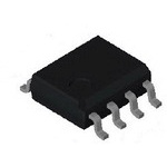
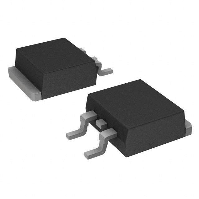
| 描述 | MOSFET N-CH 80V 7.6A 8SOICMOSFET SO-8 N-CH 80V |
| 产品分类 | FET - 单分离式半导体 |
| FET功能 | 逻辑电平门 |
| FET类型 | MOSFET N 通道,金属氧化物 |
| Id-ContinuousDrainCurrent | 7.6 A |
| Id-连续漏极电流 | 7.6 A |
| 品牌 | Fairchild Semiconductor |
| 产品手册 | |
| 产品图片 |
|
| rohs | 符合RoHS无铅 / 符合限制有害物质指令(RoHS)规范要求 |
| 产品系列 | 晶体管,MOSFET,Fairchild Semiconductor FDS3580PowerTrench® |
| 数据手册 | |
| 产品型号 | FDS3580 |
| PCN设计/规格 | |
| Pd-PowerDissipation | 2.5 W |
| Pd-功率耗散 | 2.5 W |
| RdsOn-Drain-SourceResistance | 22 mOhms |
| RdsOn-漏源导通电阻 | 22 mOhms |
| Vds-Drain-SourceBreakdownVoltage | 80 V |
| Vds-漏源极击穿电压 | 80 V |
| Vgs-Gate-SourceBreakdownVoltage | +/- 20 V |
| Vgs-栅源极击穿电压 | 20 V |
| 上升时间 | 8 ns |
| 下降时间 | 16 ns |
| 不同Id时的Vgs(th)(最大值) | 4V @ 250µA |
| 不同Vds时的输入电容(Ciss) | 1800pF @ 25V |
| 不同Vgs时的栅极电荷(Qg) | 46nC @ 10V |
| 不同 Id、Vgs时的 RdsOn(最大值) | 29 毫欧 @ 7.6A,10V |
| 产品培训模块 | http://www.digikey.cn/PTM/IndividualPTM.page?site=cn&lang=zhs&ptm=356 |
| 产品种类 | MOSFET |
| 供应商器件封装 | 8-SOIC N |
| 其它名称 | FDS3580FSDKR |
| 典型关闭延迟时间 | 34 ns |
| 功率-最大值 | 1W |
| 包装 | Digi-Reel® |
| 单位重量 | 187 mg |
| 商标 | Fairchild Semiconductor |
| 安装类型 | 表面贴装 |
| 安装风格 | SMD/SMT |
| 封装 | Reel |
| 封装/外壳 | 8-SOIC(0.154",3.90mm 宽) |
| 封装/箱体 | SOIC-8 Narrow |
| 工厂包装数量 | 2500 |
| 晶体管极性 | N-Channel |
| 最大工作温度 | + 150 C |
| 最小工作温度 | - 55 C |
| 标准包装 | 1 |
| 正向跨导-最小值 | 28 S |
| 漏源极电压(Vdss) | 80V |
| 电流-连续漏极(Id)(25°C时) | 7.6A (Ta) |
| 系列 | FDS3580 |
| 通道模式 | Enhancement |
| 配置 | Single Quad Drain Triple Source |
| 零件号别名 | FDS3580_NL |


- 商务部:美国ITC正式对集成电路等产品启动337调查
- 曝三星4nm工艺存在良率问题 高通将骁龙8 Gen1或转产台积电
- 太阳诱电将投资9.5亿元在常州建新厂生产MLCC 预计2023年完工
- 英特尔发布欧洲新工厂建设计划 深化IDM 2.0 战略
- 台积电先进制程称霸业界 有大客户加持明年业绩稳了
- 达到5530亿美元!SIA预计今年全球半导体销售额将创下新高
- 英特尔拟将自动驾驶子公司Mobileye上市 估值或超500亿美元
- 三星加码芯片和SET,合并消费电子和移动部门,撤换高东真等 CEO
- 三星电子宣布重大人事变动 还合并消费电子和移动部门
- 海关总署:前11个月进口集成电路产品价值2.52万亿元 增长14.8%


PDF Datasheet 数据手册内容提取
Is Now Part of To learn more about ON Semiconductor, please visit our website at www.onsemi.com Please note: As part of the Fairchild Semiconductor integration, some of the Fairchild orderable part numbers will need to change in order to meet ON Semiconductor’s system requirements. Since the ON Semiconductor product management systems do not have the ability to manage part nomenclature that utilizes an underscore (_), the underscore (_) in the Fairchild part numbers will be changed to a dash (-). This document may contain device numbers with an underscore (_). Please check the ON Semiconductor website to verify the updated device numbers. The most current and up-to-date ordering information can be found at www.onsemi.com. Please email any questions regarding the system integration to Fairchild_questions@onsemi.com. ON Semiconductor and the ON Semiconductor logo are trademarks of Semiconductor Components Industries, LLC dba ON Semiconductor or its subsidiaries in the United States and/or other countries. ON Semiconductor owns the rights to a number of patents, trademarks, copyrights, trade secrets, and other intellectual property. A listing of ON Semiconductor’s product/patent coverage may be accessed at www.onsemi.com/site/pdf/Patent-Marking.pdf. ON Semiconductor reserves the right to make changes without further notice to any products herein. ON Semiconductor makes no warranty, representation or guarantee regarding the suitability of its products for any particular purpose, nor does ON Semiconductor assume any liability arising out of the application or use of any product or circuit, and specifically disclaims any and all liability, including without limitation special, consequential or incidental damages. Buyer is responsible for its products and applications using ON Semiconductor products, including compliance with all laws, regulations and safety requirements or standards, regardless of any support or applications information provided by ON Semiconductor. “Typical” parameters which may be provided in ON Semiconductor data sheets and/or specifications can and do vary in different applications and actual performance may vary over time. All operating parameters, including “Typicals” must be validated for each customer application by customer’s technical experts. ON Semiconductor does not convey any license under its patent rights nor the rights of others. ON Semiconductor products are not designed, intended, or authorized for use as a critical component in life support systems or any FDA Class 3 medical devices or medical devices with a same or similar classification in a foreign jurisdiction or any devices intended for implantation in the human body. Should Buyer purchase or use ON Semiconductor products for any such unintended or unauthorized application, Buyer shall indemnify and hold ON Semiconductor and its officers, employees, subsidiaries, affiliates, and distributors harmless against all claims, costs, damages, and expenses, and reasonable attorney fees arising out of, directly or indirectly, any claim of personal injury or death associated with such unintended or unauthorized use, even if such claim alleges that ON Semiconductor was negligent regarding the design or manufacture of the part. ON Semiconductor is an Equal Opportunity/Affirmative Action Employer. This literature is subject to all applicable copyright laws and is not for resale in any manner.
F D December 2000 S 3 5 8 0 FDS3580 80V N-Channel PowerTrench MOSFET General Description Features This N-Channel MOSFET has been designed specifically • 7.6 A, 80 V. R = 0.029 Ω @ V = 10 V DS(ON) GS to improve the overall efficiency of DC/DC converters using R = 0.033 Ω @ V = 6 V. either synchronous or conventional switching PWM DS(ON) GS controllers. • Low gate charge (34nC typical). These MOSFETs feature faster switching and lower gate charge than other MOSFETs with comparable R • Fast switching speed. DS(ON) specifications. • High performance trench technology for extremely low R . The result is a MOSFET that is easy and safer to drive DS(ON) (even at very high frequencies), and DC/DC power supply • High power and current handling capability. designs with higher overall efficiency. D D 5 4 D D 6 3 7 2 G S S 8 1 SO-8 S Absolute Maximum Ratings T = 25°C unless otherwise noted A Symbol Parameter Ratings Units V Drain-Source Voltage 80 V DSS V Gate-Source Voltage ±20 V GSS ID Drain Current - Continuous (Note 1a) 7.6 A - Pulsed 50 PD Power Dissipation for Single Operation (Note 1a) 2.5 W (Note 1b) 1.2 (Note 1c) 1 T, T Operating and Storage Junction Temperature Range -55 to +150 °C J stg Thermal Characteristics RθJA Thermal Resistance, Junction-to-Ambient (Note 1a) 50 °C/W RθJC Thermal Resistance, Junction-to-Case (Note 1) 25 °C/W Package Outlines and Ordering Information Device Marking Device Reel Size Tape Width Quantity FDS3580 FDS3580 13’’ 12mm 2500 units 2000 Fairchild Semiconductor International FDS3580 Rev. C
F D Electrical Characteristics T = 25°C unless otherwise noted S A 3 Symbol Parameter Test Conditions Min Typ Max Units 5 8 0 Drain-Source Avalanche Ratings (Note 2) W Single Pulse Drain-Source V = 40 V, I = 7.6 A 245 mJ DSS DD D Avalanche Energy I Maximum Drain-Source Avalanche Current 7.6 A AR Off Characteristics BVDSS Drain-Source Breakdown Voltage VGS = 0 V, ID = 250 µA 80 V ∆BVDSS Breakdown Voltage Temperature ID = 250 µA, Referenced to 25°C 81 mV/°C ∆T Coefficient J IDSS Zero Gate Voltage Drain Current VDS = 64 V, VGS = 0 V 1 µA I Gate-Body Leakage, Forward V = 20 V, V = 0 V 100 nA GSSF GS DS I Gate-Body Leakage, Reverse V = -20 V, V = 0 V -100 nA GSSR GS DS On Characteristics (Note 2) VGS(th) Gate Threshold Voltage VDS = VGS, ID = 250 µA 2 2.5 4 V ∆VGS(th) Gate Threshold Voltage ID = 250 µA, Referenced to 25°C -7 mV/°C ∆T Temperature Coefficient J R Static Drain-Source V = 10 V, I = 7.6 A 0.022 0.029 Ω DS(on) GS D On-Resistance V = 10 V, I = 7.6 A, T=125°C 0.037 0.055 GS D J V = 6 V, I = 7 A 0.024 0.033 GS D I On-State Drain Current V = 10 V, V = 5 V 30 A D(on) GS DS g Forward Transconductance V = 5 V, I = 7.6 A 28 S FS DS D Dynamic Characteristics C Input Capacitance V = 25 V, V = 0 V, 1800 pF iss DS GS f = 1.0 MHz C Output Capacitance 180 pF oss C Reverse Transfer Capacitance 90 pF rss Switching Characteristics (Note 2) t Turn-On Delay Time V = 40 V, I = 1 A, 13 26 ns d(on) DD D Ω tr Turn-On Rise Time VGS = 10 V, RGEN = 6 8 20 ns t Turn-Off Delay Time 34 60 ns d(off) t Turn-Off Fall Time 16 30 ns f Q Total Gate Charge V = 40 V, I = 7.6 A, 34 46 nC g DS D V = 10 V Q Gate-Source Charge GS 6.1 nC gs Q Gate-Drain Charge 6.9 nC gd Drain-Source Diode Characteristics and Maximum Ratings I Maximum Continuous Drain-Source Diode Forward Current 2.1 A S VSD Drain-Source Diode Forward Voltage VGS = 0 V, IS = 2.1 A (Note 2) 0.74 1.2 V Notes: 1: RθJA is the sum of the junction-to-case and case-to-ambient resistance where the case thermal reference is defined as the solder mounting surface of the drain pins. RθJC is guaranteed by design while RθCA is determined by the user's board design. a) 50° C/W when b) 105° C/W when c) 125° C/W when mounted on a 1 in2 mounted on a 0.04 in2 mounted on a minimum pad of 2 oz. copper. pad of 2 oz. copper. pad. Scale 1 : 1 on letter size paper 2: Pulse Test: Pulse Width ≤ 300 µs, Duty Cycle ≤ 2.0% FDS3580 Rev. C
F D Typical Characteristics S 3 5 8 60 VGS = 10V E 2 0 50 6.0V 5.0V NC1.8 RRENT (A) 40 4.5V MALIZEDN-RESISTA1.6 VGS = 4.0V I, DRAIN CUD123000 4.0V R, NORDS(ON)AIN-SOURCE O11..124 4.5V 5.0V 6.0V 7.0V 10V R 3.5V D 0 0.8 0 1 2 3 4 5 0 10 20 30 40 50 60 VDS, DRAIN-SOURCE VOLTAGE (V) ID, DIRAIN CURRENT (A) Figure 1. On-Region Characteristics. Figure 2. On-Resistance Variation with Drain Current and Gate Voltage. 2 0.06 ANCE1.8 VIDG S= =7 .160AV HM) 0.05 ID = 3.8A ORMALIZEDE ON-RESIST111...246 SISTANCE (O 00..0034 TA = 125oC NC E R, DS(ON)DRAIN-SOUR00..681 R, ON-RDS(ON)00..0012 TA = 25oC 0.4 0 -50 -25 0 25 50 75 100 125 150 3 4 5 6 7 8 9 10 TJ, JUNCTION TEMPERATURE (oC) VGS, GATE TO SOURCE VOLTAGE (V) Figure 3. On-Resistance Variation Figure 4. On-Resistance Variation with Temperature. with Gate-to-Source Voltage. 60 100 VDS = 5V TA = -55oC 25oC A) VGS = 0V 50 T ( 10 A) 125oC EN RRENT ( 40 N CURR 1 TA = 125oC 25oC AIN CU 30 E DRAI 0.1 -55oC I, DRD20 EVERS 0.01 10 R 0.001 I, S 0 0.0001 2 3 4 5 6 0 0.2 0.4 0.6 0.8 1 1.2 1.4 VGS, GATE TO SOURCE VOLTAGE (V) VSD, BODY DIODE FORWARD VOLTAGE (V) Figure 5. Transfer Characteristics. Figure 6. Body Diode Forward Voltage Variation with Source Current and Temperature. FDS3580 Rev. C
F D Typical Characteristics S (continued) 3 5 8 10 2400 0 GE (V) 8 ID = 7.6A VDS = 10V 40V20V 2000 Vf G=S 1 =M 0H Vz VOLTA 6 E (pF)1600 CISS SOURCE 4 ACITANC1200 ATE- CAP 800 V, GGS 2 400 COSS CRSS 0 0 0 5 10 15 20 25 30 35 0 10 20 30 40 50 60 70 80 Qg, GATE CHARGE (nC) VDS, DRAIN TO SOURCE VOLTAGE (V) Figure 7. Gate-Charge Characteristics. Figure 8. Capacitance Characteristics. 100 50 T (A) 10 RDS(ON) LIMIT 10m1sms100µs 40 SRINθ J TGA A =L =1E 22 P55°U°CCL/SWE N RE 100ms W)30 I, DRAIN CURD 0.11 SRIθNJVAG G=LS E1= 2 P15U0oCVL/SWE DC10s1s POWER (1200 TA = 25oC 0.01 0 0.1 1 10 100 0.001 0.01 0.1 1 10 100 300 VDS, DRAIN-SOURCE VOLTAGE (V) SINGLE PULSE TIME (SEC) Figure 9. Maximum Safe Operating Area. Figure 10. Single Pulse Maximum Power Dissipation. E 1 D EFFECTIVEMAL RESISTANC 0.0000...5125 D = 0 . 50. 2 0 .1 0 .05 P(p k )R θ R J A θ J ( tA ) = = 1r(2t)5 °*C R/ W θ J A r(t), NORMALIZERANSI ENT THER 0000..00..00001225 0.02 0 .01 S i n g le P u l s e D uT tJ -y T t A1 C =ty 2 P c l* e R, θD J A = (t )t1 /t2 T 0.001 0.0001 0.001 0.01 0.1 1 10 100 300 t 1 , TIM E (se c) Figure 11. Transient Thermal Response Curve. Thermal characterization performed using the conditions described in Note 1c. Transient themal response will change depending on the circuit board design. FDS3580 Rev. C
TRADEMARKS The following are registered and unregistered trademarks Fairchild Semiconductor owns or is authorized to use and is not intended to be an exhaustive list of all such trademarks. ACEx™ FASTr™ PowerTrench SyncFET™ Bottomless™ GlobalOptoisolator™ QFET™ TinyLogic™ CoolFET™ GTO™ QS™ UHC™ CROSSVOLT™ HiSeC™ QT Optoelectronics™ VCX™ DOME™ ISOPLANAR™ Quiet Series™ E2CMOSTM MICROWIRE™ SILENT SWITCHER EnSignaTM OPTOLOGIC™ SMART START™ FACT™ OPTOPLANAR™ SuperSOT™-3 FACT Quiet Series™ PACMAN™ SuperSOT™-6 FAST POP™ SuperSOT™-8 DISCLAIMER FAIRCHILD SEMICONDUCTOR RESERVES THE RIGHT TO MAKE CHANGES WITHOUT FURTHER NOTICE TO ANY PRODUCTS HEREIN TO IMPROVE RELIABILITY, FUNCTION OR DESIGN. FAIRCHILD DOES NOT ASSUME ANY LIABILITY ARISING OUT OF THE APPLICATION OR USE OF ANY PRODUCT OR CIRCUIT DESCRIBED HEREIN; NEITHER DOES IT CONVEY ANY LICENSE UNDER ITS PATENT RIGHTS, NOR THE RIGHTS OF OTHERS. LIFE SUPPORT POLICY FAIRCHILD’S PRODUCTS ARE NOT AUTHORIZED FOR USE AS CRITICAL COMPONENTS IN LIFE SUPPORT DEVICES OR SYSTEMS WITHOUT THE EXPRESS WRITTEN APPROVAL OF FAIRCHILD SEMICONDUCTOR CORPORATION. As used herein: 1. Life support devices or systems are devices or 2. A critical component is any component of a life systems which, (a) are intended for surgical implant into support device or system whose failure to perform can the body, or (b) support or sustain life, or (c) whose be reasonably expected to cause the failure of the life failure to perform when properly used in accordance support device or system, or to affect its safety or with instructions for use provided in the labeling, can be effectiveness. reasonably expected to result in significant injury to the user. PRODUCT STATUS DEFINITIONS Definition of Terms Datasheet Identification Product Status Definition Advance Information Formative or This datasheet contains the design specifications for In Design product development. Specifications may change in any manner without notice. Preliminary First Production This datasheet contains preliminary data, and supplementary data will be published at a later date. Fairchild Semiconductor reserves the right to make changes at any time without notice in order to improve design. No Identification Needed Full Production This datasheet contains final specifications. Fairchild Semiconductor reserves the right to make changes at any time without notice in order to improve design. Obsolete Not In Production This datasheet contains specifications on a product that has been discontinued by Fairchild semiconductor. The datasheet is printed for reference information only. Rev. G
ON Semiconductor and are trademarks of Semiconductor Components Industries, LLC dba ON Semiconductor or its subsidiaries in the United States and/or other countries. ON Semiconductor owns the rights to a number of patents, trademarks, copyrights, trade secrets, and other intellectual property. A listing of ON Semiconductor’s product/patent coverage may be accessed at www.onsemi.com/site/pdf/Patent−Marking.pdf. ON Semiconductor reserves the right to make changes without further notice to any products herein. ON Semiconductor makes no warranty, representation or guarantee regarding the suitability of its products for any particular purpose, nor does ON Semiconductor assume any liability arising out of the application or use of any product or circuit, and specifically disclaims any and all liability, including without limitation special, consequential or incidental damages. Buyer is responsible for its products and applications using ON Semiconductor products, including compliance with all laws, regulations and safety requirements or standards, regardless of any support or applications information provided by ON Semiconductor. “Typical” parameters which may be provided in ON Semiconductor data sheets and/or specifications can and do vary in different applications and actual performance may vary over time. All operating parameters, including “Typicals” must be validated for each customer application by customer’s technical experts. ON Semiconductor does not convey any license under its patent rights nor the rights of others. ON Semiconductor products are not designed, intended, or authorized for use as a critical component in life support systems or any FDA Class 3 medical devices or medical devices with a same or similar classification in a foreign jurisdiction or any devices intended for implantation in the human body. Should Buyer purchase or use ON Semiconductor products for any such unintended or unauthorized application, Buyer shall indemnify and hold ON Semiconductor and its officers, employees, subsidiaries, affiliates, and distributors harmless against all claims, costs, damages, and expenses, and reasonable attorney fees arising out of, directly or indirectly, any claim of personal injury or death associated with such unintended or unauthorized use, even if such claim alleges that ON Semiconductor was negligent regarding the design or manufacture of the part. ON Semiconductor is an Equal Opportunity/Affirmative Action Employer. This literature is subject to all applicable copyright laws and is not for resale in any manner. PUBLICATION ORDERING INFORMATION LITERATURE FULFILLMENT: N. American Technical Support: 800−282−9855 Toll Free ON Semiconductor Website: www.onsemi.com Literature Distribution Center for ON Semiconductor USA/Canada 19521 E. 32nd Pkwy, Aurora, Colorado 80011 USA Europe, Middle East and Africa Technical Support: Order Literature: http://www.onsemi.com/orderlit Phone: 303−675−2175 or 800−344−3860 Toll Free USA/Canada Phone: 421 33 790 2910 Fax: 303−675−2176 or 800−344−3867 Toll Free USA/Canada Japan Customer Focus Center For additional information, please contact your local Email: orderlit@onsemi.com Phone: 81−3−5817−1050 Sales Representative © Semiconductor Components Industries, LLC www.onsemi.com www.onsemi.com 1
Mouser Electronics Authorized Distributor Click to View Pricing, Inventory, Delivery & Lifecycle Information: O N Semiconductor: FDS3580