ICGOO在线商城 > 分立半导体产品 > 晶体管 - FET,MOSFET - 单 > STW13NK100Z
 Datasheet下载
- 型号: STW13NK100Z
- 制造商: STMicroelectronics
- 库位|库存: xxxx|xxxx
- 要求:
| 数量阶梯 | 香港交货 | 国内含税 |
| +xxxx | $xxxx | ¥xxxx |
查看当月历史价格
查看今年历史价格
STW13NK100Z产品简介:
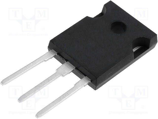
ICGOO电子元器件商城为您提供STW13NK100Z由STMicroelectronics设计生产,在icgoo商城现货销售,并且可以通过原厂、代理商等渠道进行代购。 STW13NK100Z价格参考¥17.27-¥21.16。STMicroelectronicsSTW13NK100Z封装/规格:晶体管 - FET,MOSFET - 单, 通孔 N 沟道 1000V 13A(Tc) 350W(Tc) TO-247-3。您可以下载STW13NK100Z参考资料、Datasheet数据手册功能说明书,资料中有STW13NK100Z 详细功能的应用电路图电压和使用方法及教程。
STMicroelectronics(意法半导体)的型号 STW13NK100Z 是一款 N 沟道增强型 MOSFET,属于晶体管 - FET、MOSFET - 单类别的产品。以下是其主要应用场景及特点:

 应用场景:
1. 开关电源(SMPS)
   - 该 MOSFET 适用于开关电源中的高频开关应用,例如 DC-DC 转换器、AC-DC 转换器和功率因数校正(PFC)电路。
   - 其高耐压能力(1000V)使其适合高压输入环境。

2. 电机驱动
   - 在工业控制或家电领域中,可用于驱动中小型电机,例如空调风扇、洗衣机泵或电动工具。
   - 提供高效能的开关性能以减少能量损耗。

3. 逆变器
   - 用于太阳能逆变器或其他类型的电力逆变器中,将直流电转换为交流电。
   - 高击穿电压和低导通电阻有助于提高逆变效率。

4. 负载开关与保护电路
   - 可作为负载开关,用于开启或关闭高电压设备。
   - 在过流保护、短路保护等电路中起到关键作用。

5. 电磁阀与继电器驱动
   - 适用于需要高电压驱动的电磁阀或继电器控制场合。
   - 提供稳定的电流输出以确保器件正常工作。

6. 不间断电源(UPS)系统
   - 在 UPS 系统中用于电池充放电管理及电压调节。
   - 高可靠性设计可满足长时间运行需求。

 特点总结:
- 高耐压:额定电压高达 1000V,适合高压环境。
- 低导通电阻:降低功耗并提升效率。
- 快速开关速度:减少开关损耗,适应高频应用。
- 高可靠性:具备良好的热稳定性和抗干扰能力。

总之,STW13NK100Z 广泛应用于需要高电压、高效率和可靠性的电力电子设备中,是工业自动化、家用电器、新能源等领域的重要元件。
| 参数 | 数值 |
| 产品目录 | |
| ChannelMode | Enhancement |
| 描述 | MOSFET N-CH 1KV 13A TO-247MOSFET N-Ch 1000 Volt 13A Zener SuperMESH |
| 产品分类 | FET - 单分离式半导体 |
| FET功能 | 标准 |
| FET类型 | MOSFET N 通道,金属氧化物 |
| Id-ContinuousDrainCurrent | 13 A |
| Id-连续漏极电流 | 13 A |
| 品牌 | STMicroelectronics |
| 产品手册 | |
| 产品图片 |
|
| rohs | 符合RoHS无铅 / 符合限制有害物质指令(RoHS)规范要求 |
| 产品系列 | 晶体管,MOSFET,STMicroelectronics STW13NK100ZSuperMESH™ |
| 数据手册 | |
| 产品型号 | STW13NK100Z |
| Pd-PowerDissipation | 350 W |
| Pd-功率耗散 | 350 W |
| Qg-GateCharge | 190 nC |
| Qg-栅极电荷 | 190 nC |
| RdsOn-Drain-SourceResistance | 700 mOhms |
| RdsOn-漏源导通电阻 | 700 mOhms |
| Vds-Drain-SourceBreakdownVoltage | 1 kV |
| Vds-漏源极击穿电压 | 1 kV |
| Vgs-Gate-SourceBreakdownVoltage | +/- 30 V |
| Vgs-栅源极击穿电压 | 30 V |
| 上升时间 | 35 ns |
| 下降时间 | 45 ns |
| 不同Id时的Vgs(th)(最大值) | 4.5V @ 150µA |
| 不同Vds时的输入电容(Ciss) | 6000pF @ 25V |
| 不同Vgs时的栅极电荷(Qg) | 266nC @ 10V |
| 不同 Id、Vgs时的 RdsOn(最大值) | 700 毫欧 @ 6.5A,10V |
| 产品种类 | MOSFET |
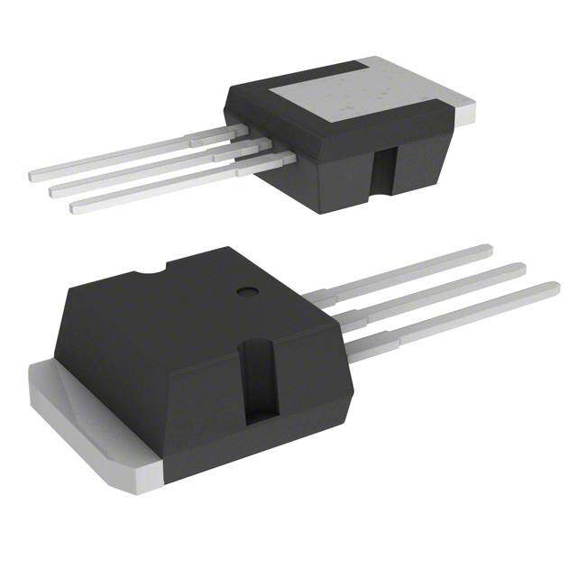
| 供应商器件封装 | TO-247-3 |
| 其它名称 | 497-3556-5 |
| 其它有关文件 | http://www.st.com/web/catalog/sense_power/FM100/CL824/SC1168/PF67503?referrer=70071840 |
| 典型关闭延迟时间 | 145 ns |
| 功率-最大值 | 350W |
| 包装 | 管件 |
| 商标 | STMicroelectronics |
| 安装类型 | 通孔 |
| 安装风格 | Through Hole |
| 封装 | Tube |
| 封装/外壳 | TO-247-3 |
| 封装/箱体 | TO-247-3 |
| 工具箱 | /product-detail/zh/497-8004-KIT/497-8004-KIT-ND/811050 |
| 工厂包装数量 | 30 |
| 晶体管极性 | N-Channel |
| 最大工作温度 | + 150 C |
| 最小工作温度 | - 55 C |
| 标准包装 | 30 |
| 漏源极电压(Vdss) | 1000V(1kV) |
| 电流-连续漏极(Id)(25°C时) | 13A (Tc) |
| 系列 | STW13NK100Z |
| 通道模式 | Enhancement |
| 配置 | Single |


PDF Datasheet 数据手册内容提取
STW11NK100Z STW13NK100Z Ω N-channel 1000V - 0.56 - 13A - TO-247 Zener - Protected SuperMESH™ PowerMOSFET General features V Type DSS R I P (@Tjmax) DS(on) D W STW13NK100Z 1000 V < 0.70 Ω 13 A 350W ■ Extremely high dv/dt capability ■ 100% avalanche tested ■ Gate charge minimized TO-247 ■ Very low intrinsic capacitances ■ Very good manufacturing repeatibility Description The SuperMESH™ series is obtained through an Internal schematic diagram extreme optimization of ST’s well established strip-based PowerMESH™ layout. In addition to pushing on-resistance significantly down, special care is taken to ensure a very good dv/dt capability for the most demanding applications. Such series complements ST full range of high voltage MOSFETs including revolutionary MDmesh™ products. Applications ■ Switching application Order codes Part number Marking Package Packaging STW13NK100Z W13NK100Z TO-247 Tube August 2006 Rev 5 1/14 www.st.com 14
Contents STW13NK100Z Contents 1 Electrical ratings . . . . . . . . . . . . . . . . . . . . . . . . . . . . . . . . . . . . . . . . . . . . 3 1.1 Protection features of gate-to-source zener diodes . . . . . . . . . . . . . . . . . . 4 2 Electrical characteristics . . . . . . . . . . . . . . . . . . . . . . . . . . . . . . . . . . . . . 5 2.1 Electrical characteristics (curves) . . . . . . . . . . . . . . . . . . . . . . . . . . . . 7 3 Test circuit . . . . . . . . . . . . . . . . . . . . . . . . . . . . . . . . . . . . . . . . . . . . . . . 10 4 Package mechanical data . . . . . . . . . . . . . . . . . . . . . . . . . . . . . . . . . . . . 11 5 Revision history . . . . . . . . . . . . . . . . . . . . . . . . . . . . . . . . . . . . . . . . . . . 13 2/14
STW13NK100Z Electrical ratings 1 Electrical ratings Table 1. Absolute maximum ratings Symbol Parameter Value Unit V Drain-source voltage (V = 0) 1000 V DS GS V Drain-gate voltage (R = 20KΩ) 1000 V DGR GS V Gate-source voltage ± 30 V GS I Drain current (continuous) at T = 25°C 13 A D C I Drain current (continuous) at T =100°C 8.2 A D C I (1) Drain current (pulsed) 52 A DM P Total dissipation at T = 25°C 350 W TOT C Derating Factor 2.7 W/°C V Gate source ESD(HBM-C=100pF, R=1,5KΩ) 6000 V ESD (G-S) dv/dt(2) Peak diode recovery voltage slope 4 V/ns TJ Operating junction temperature -55 to 150 °C T Storage temperature stg 1. Pulse width limited by safe operating area 2. I ≤ 8.3 A, di/dt ≤ 200A/µs, V ≤ V , T ≤ T SD DD (BR)DSS j JMAX Table 2. Thermal data Symbol Parameter Value Unit R Thermal resistance junction-case Max 0.36 °C/W thj-case R Thermal resistance junction-ambient Max 50 °C/W thj-a Maximum lead temperature for soldering T 300 °C l purpose Table 3. Avalanche characteristics Symbol Parameter Value Unit Avalanche current, repetitive or not-repetitive I 13 A AR (pulse width limited by Tj Max) Single pulse avalanche energy E 700 mJ AS (starting Tj=25°C, Id=Iar, Vdd=50V) 3/14
Electrical ratings STW13NK100Z Table 4. Gate-source zener diode Symbol Parameter Test conditions Min. Typ. Max. Unit BV Gate-source breakdown voltage Igs=± 1mA (Open Drain) 30 V GSO 1.1 Protection features of gate-to-source zener diodes The built-in back-to-back Zener diodes have specifically been designed to enhance not only the device’s ESD capability, but also to make them safely absorb possible voltage transients that may occasionally be applied from gate to source. In this respect the Zener voltage is appropriate to achieve an efficient and cost-effective intervention to protect the device’s integrity. These integrated Zener diodes thus avoid the usage of external components. 4/14
STW13NK100Z Electrical characteristics 2 Electrical characteristics (T =25°C unless otherwise specified) CASE Table 5. On/off states Symbol Parameter Test conditions Min. Typ. Max. Unit Drain-source breakdown V I = 1mA, V = 0 1000 V (BR)DSS voltage D GS V = Max rating, Zero gate voltage drain DS 1 µA I V = Max rating, DSS current (VGS = 0) DS 10 µA Tc = 125°C Gate body leakage current IGSS (V = 0) VGS = ± 20V ±10 µA GS V Gate threshold voltage V = V , I = 150 µA 3 3.75 4.5 V GS(th) DS GS D Static drain-source on R V = 10V, I = 6.5 A 0.56 0.70 Ω DS(on) resistance GS D Table 6. Dynamic Symbol Parameter Test conditions Min. Typ. Max. Unit g (1) Forward transconductance V =15V, I = 6.5 A 14 S fs DS D Input capacitance C 6000 pF iss Output capacitance C V =25V, f=1 MHz, V =0 455 pF oss DS GS Reverse transfer C 100 pF rss capacitance Equivalent output C (2) V =0, V =0V to 800V 227 pF osseq . capacitance GS DS t Turn-on delay time 45 ns d(on) V =500 V, I = 7A, t Rise time DD D 35 ns r R =4.7Ω, V =10V t Off-voltage rise time G GS 145 ns d(off) (see Figure16) t Fall time 45 ns f Q Total gate charge 190 266 nC g V =800V, I = 13A Q Gate-source charge DD D 30 nC gs V =10V Q Gate-drain charge GS 100 nC gd 1. Pulsed: pulse duration=300µs, duty cycle 1.5% 2. C is defined as a constant equivalent capacitance giving the same charging time as C when V oss eq. oss DS increases from 0 to 80% V DSS 5/14
Electrical characteristics STW13NK100Z Table 7. Source drain diode Symbol Parameter Test conditions Min Typ. Max Unit I Source-drain current 13 A SD I (1) Source-drain current (pulsed) 52 A SDM V (2) Forward on voltage I =8.3A, V =0 1.6 V SD SD GS I =13 A, t Reverse recovery time SD 820 ns rr di/dt = 100A/µs, Q Reverse recovery charge 12.7 µC rr V =100 V, Tj=25°C I Reverse recovery current DD 31 A RRM (see Figure18) I =13 A, t Reverse recovery time SD 1050 ns rr di/dt = 100A/µs, Q Reverse recovery charge 17.8 µC rr V =100V, Tj=150°C I Reverse recovery current DD 34 A RRM (see Figure18) 1. Pulse width limited by safe operating area 2. Pulsed: pulse duration=300µs, duty cycle 1.5% 6/14
STW13NK100Z Electrical characteristics 2.1 Electrical characteristics (curves) Figure 1. Safe operating area Figure 2. Thermal impedance Figure 3. Output characterisics Figure 4. Transfer characteristics 7/14
Electrical characteristics STW13NK100Z Figure 5. Transconductance Figure 6. Static drain-source on resistance Figure 7. Gate charge vs gate-source voltage Figure 8. Capacitance variations Figure 9. Normalized gate threshold voltage Figure 10. Normalized on resistance vs vs temperature temperature 8/14
STW13NK100Z Electrical characteristics Figure 11. Source-drain diode forward Figure 12. Normalized B vs temperature VDSS characteristics Figure 13. Maximum avalanche energy vs temperature 9/14
Test circuit STW13NK100Z 3 Test circuit Figure 14. Unclamped Inductive load test Figure 15. Unclamped Inductive waveform circuit Figure 16. Switching times test circuit for Figure 17. Gate charge test circuit resistive load Figure 18. Test circuit for inductive load switching and diode recovery times 10/14
STW13NK100Z Package mechanical data 4 Package mechanical data In order to meet environmental requirements, ST offers these devices in ECOPACK® packages. These packages have a Lead-free second level interconnect . The category of second level interconnect is marked on the package and on the inner box label, in compliance with JEDEC Standard JESD97. The maximum ratings related to soldering conditions are also marked on the inner box label. ECOPACK is an ST trademark. ECOPACK specifications are available at: www.st.com 11/14
Package mechanical data STW13NK100Z TO-247 MECHANICAL DATA mm. inch DIM. MIN. TYP MAX. MIN. TYP. MAX. A 4.85 5.15 0.19 0.20 A1 2.20 2.60 0.086 0.102 b 1.0 1.40 0.039 0.055 b1 2.0 2.40 0.079 0.094 b2 3.0 3.40 0.118 0.134 c 0.40 0.80 0.015 0.03 D 19.85 20.15 0.781 0.793 E 15.45 15.75 0.608 0.620 e 5.45 0.214 L 14.20 14.80 0.560 0.582 L1 3.70 4.30 0.14 0.17 L2 18.50 0.728 øP 3.55 3.65 0.140 0.143 øR 4.50 5.50 0.177 0.216 S 5.50 0.216 12/14
STW13NK100Z Revision history 5 Revision history Table 8. Revision history Date Revision Changes 22-Jun-2004 1 Target document 09-Sep-2004 2 Preliminary document 28-Jan-2005 3 Complete version with curves 18-Sep-2005 4 Figure12 changed 01-Aug-2006 5 New template, no content change 13/14
STW13NK100Z Please Read Carefully: Information in this document is provided solely in connection with ST products. STMicroelectronics NV and its subsidiaries (“ST”) reserve the right to make changes, corrections, modifications or improvements, to this document, and the products and services described herein at any time, without notice. All ST products are sold pursuant to ST’s terms and conditions of sale. Purchasers are solely responsible for the choice, selection and use of the ST products and services described herein, and ST assumes no liability whatsoever relating to the choice, selection or use of the ST products and services described herein. No license, express or implied, by estoppel or otherwise, to any intellectual property rights is granted under this document. If any part of this document refers to any third party products or services it shall not be deemed a license grant by ST for the use of such third party products or services, or any intellectual property contained therein or considered as a warranty covering the use in any manner whatsoever of such third party products or services or any intellectual property contained therein. UNLESS OTHERWISE SET FORTH IN ST’S TERMS AND CONDITIONS OF SALE ST DISCLAIMS ANY EXPRESS OR IMPLIED WARRANTY WITH RESPECT TO THE USE AND/OR SALE OF ST PRODUCTS INCLUDING WITHOUT LIMITATION IMPLIED WARRANTIES OF MERCHANTABILITY, FITNESS FOR A PARTICULAR PURPOSE (AND THEIR EQUIVALENTS UNDER THE LAWS OF ANY JURISDICTION), OR INFRINGEMENT OF ANY PATENT, COPYRIGHT OR OTHER INTELLECTUAL PROPERTY RIGHT. UNLESS EXPRESSLY APPROVED IN WRITING BY AN AUTHORIZED ST REPRESENTATIVE, ST PRODUCTS ARE NOT RECOMMENDED, AUTHORIZED OR WARRANTED FOR USE IN MILITARY, AIR CRAFT, SPACE, LIFE SAVING, OR LIFE SUSTAINING APPLICATIONS, NOR IN PRODUCTS OR SYSTEMS WHERE FAILURE OR MALFUNCTION MAY RESULT IN PERSONAL INJURY, DEATH, OR SEVERE PROPERTY OR ENVIRONMENTAL DAMAGE. ST PRODUCTS WHICH ARE NOT SPECIFIED AS "AUTOMOTIVE GRADE" MAY ONLY BE USED IN AUTOMOTIVE APPLICATIONS AT USER’S OWN RISK. Resale of ST products with provisions different from the statements and/or technical features set forth in this document shall immediately void any warranty granted by ST for the ST product or service described herein and shall not create or extend in any manner whatsoever, any liability of ST. ST and the ST logo are trademarks or registered trademarks of ST in various countries. Information in this document supersedes and replaces all information previously supplied. The ST logo is a registered trademark of STMicroelectronics. All other names are the property of their respective owners. © 2006 STMicroelectronics - All rights reserved STMicroelectronics group of companies Australia - Belgium - Brazil - Canada - China - Czech Republic - Finland - France - Germany - Hong Kong - India - Israel - Italy - Japan - Malaysia - Malta - Morocco - Singapore - Spain - Sweden - Switzerland - United Kingdom - United States of America www.st.com 14/14
Mouser Electronics Authorized Distributor Click to View Pricing, Inventory, Delivery & Lifecycle Information: S TMicroelectronics: STW13NK100Z