ICGOO在线商城 > 分立半导体产品 > 晶体管 - 双极 (BJT) - 阵列 > PBSS4350SPN,115
 Datasheet下载
- 型号: PBSS4350SPN,115
- 制造商: NXP Semiconductors
- 库位|库存: xxxx|xxxx
- 要求:
| 数量阶梯 | 香港交货 | 国内含税 |
| +xxxx | $xxxx | ¥xxxx |
查看当月历史价格
查看今年历史价格
PBSS4350SPN,115产品简介:
ICGOO电子元器件商城为您提供PBSS4350SPN,115由NXP Semiconductors设计生产,在icgoo商城现货销售,并且可以通过原厂、代理商等渠道进行代购。 PBSS4350SPN,115价格参考¥询价-¥询价。NXP SemiconductorsPBSS4350SPN,115封装/规格:晶体管 - 双极 (BJT) - 阵列, Bipolar (BJT) Transistor Array NPN, PNP 50V 2.7A 750mW Surface Mount 8-SO。您可以下载PBSS4350SPN,115参考资料、Datasheet数据手册功能说明书,资料中有PBSS4350SPN,115 详细功能的应用电路图电压和使用方法及教程。
Nexperia USA Inc.的PBSS4350SPN,115是一款双极性晶体管(BJT)阵列器件,适用于多种电子电路设计。该器件具有高性能和高可靠性,广泛应用于以下场景:

1. 电源管理与开关电路:由于其高电流增益和低饱和电压特性,适用于DC-DC转换器、负载开关及电源控制模块。

2. 电机驱动与继电器控制:适合用于小型电机、电磁阀、继电器等感性负载的驱动电路中,提供稳定可靠的开关功能。

3. 工业自动化系统:在PLC、传感器接口、工业控制板中作为信号放大或隔离元件使用。

4. 汽车电子:符合AEC-Q101标准,适用于车载照明、电动窗、风扇控制等应用场景。

5. 消费类电子产品:如智能家电、音响设备、LED驱动等需要高效能晶体管的场合。

6. 逻辑电平转换与缓冲:内置多个晶体管单元,可实现多路信号处理与逻辑电平转换,适用于数字电路设计。

综上,PBSS4350SPN,115凭借其集成度高、封装小巧、性能稳定等优点,在工业、汽车及消费类领域均有广泛应用。
| 参数 | 数值 |
| 产品目录 | |
| 描述 | TRANS NPN/PNP 50V 2.7A 8SO W/RES两极晶体管 - BJT TRANS BISS TAPE-7 |
| 产品分类 | 晶体管(BJT) - 阵列分离式半导体 |
| 品牌 | NXP Semiconductors |
| 产品手册 | |
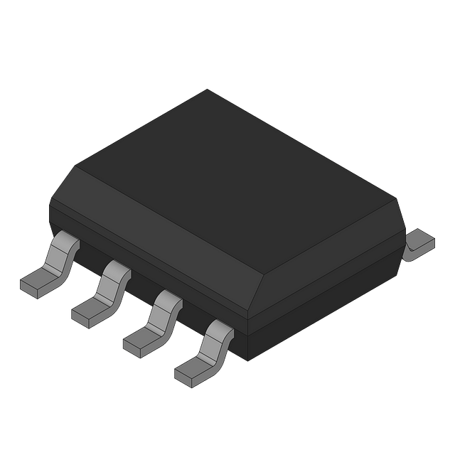
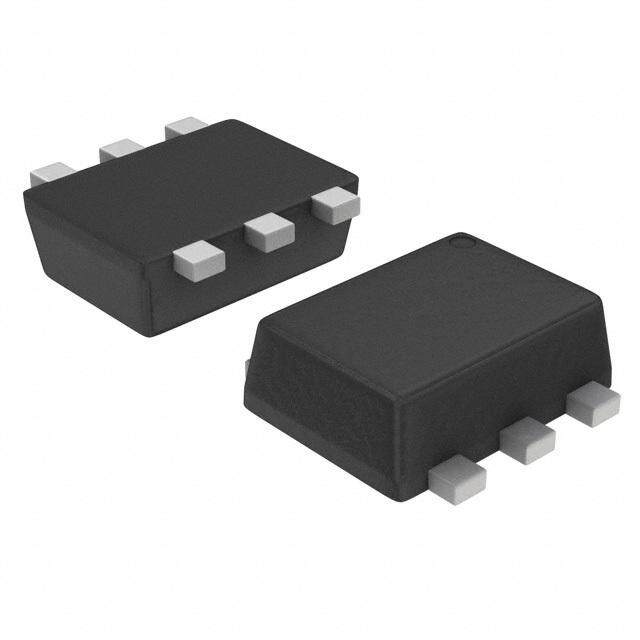
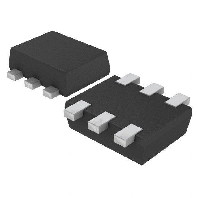
| 产品图片 |
|
| rohs | 符合RoHS无铅 / 符合限制有害物质指令(RoHS)规范要求 |
| 产品系列 | 晶体管,两极晶体管 - BJT,NXP Semiconductors PBSS4350SPN,115- |
| 数据手册 | |
| 产品型号 | PBSS4350SPN,115 |
| PCN组件/产地 | |
| 不同 Ib、Ic时的 Vce饱和值(最大值) | 340mV @ 270mA,2.7A / 370mV @ 270mA,2.7A |
| 不同 Ic、Vce 时的DC电流增益(hFE)(最小值) | 300 @ 1A,2V / 180 @ 1A,2V |
| 产品种类 | 两极晶体管 - BJT |
| 供应商器件封装 | 8-SO |
| 其它名称 | 568-7301-1 |
| 功率-最大值 | 750mW |
| 包装 | 剪切带 (CT) |
| 发射极-基极电压VEBO | 5 V |
| 商标 | NXP Semiconductors |
| 安装类型 | 表面贴装 |
| 安装风格 | SMD/SMT |
| 封装 | Reel |
| 封装/外壳 | 8-SOIC(0.154",3.90mm 宽) |
| 封装/箱体 | SO |
| 工厂包装数量 | 1000 |
| 晶体管极性 | NPN/PNP |
| 晶体管类型 | NPN,PNP |
| 最大功率耗散 | 1430 mW |
| 最大工作温度 | + 150 C |
| 最大直流电集电极电流 | 2.7 A |
| 最小工作温度 | - 65 C |
| 标准包装 | 1 |
| 特色产品 | http://www.digikey.com/cn/zh/ph/NXP/I2C.html |
| 电压-集射极击穿(最大值) | 50V |
| 电流-集电极(Ic)(最大值) | 2.7A |
| 电流-集电极截止(最大值) | 100nA |
| 直流电流增益hFE最大值 | 300 at 100 mA at 2 V |
| 配置 | Dual |
| 集电极—发射极最大电压VCEO | 50 V |
| 集电极—基极电压VCBO | 50 V |
| 零件号别名 | PBSS4350SPN T/R |
| 频率-跃迁 | - |


- 商务部:美国ITC正式对集成电路等产品启动337调查
- 曝三星4nm工艺存在良率问题 高通将骁龙8 Gen1或转产台积电
- 太阳诱电将投资9.5亿元在常州建新厂生产MLCC 预计2023年完工
- 英特尔发布欧洲新工厂建设计划 深化IDM 2.0 战略
- 台积电先进制程称霸业界 有大客户加持明年业绩稳了
- 达到5530亿美元!SIA预计今年全球半导体销售额将创下新高
- 英特尔拟将自动驾驶子公司Mobileye上市 估值或超500亿美元
- 三星加码芯片和SET,合并消费电子和移动部门,撤换高东真等 CEO
- 三星电子宣布重大人事变动 还合并消费电子和移动部门
- 海关总署:前11个月进口集成电路产品价值2.52万亿元 增长14.8%


PDF Datasheet 数据手册内容提取
PBSS4350SPN 50 V, 2.7 A NPN/PNP low V (BISS) transistor CEsat Rev. 01 — 5 April 2007 Product data sheet 1. Product profile 1.1 General description NPN/PNP double low V Breakthrough In Small Signal (BISS) transistor in a medium CEsat power Surface-Mounted Device (SMD) plastic package. Table 1. Product overview Type number Package NPN/NPN PNP/PNP complement complement NXP Name PBSS4350SPN SOT96-1 SO8 PBSS4350SS PBSS5350SS 1.2 Features n Low collector-emitter saturation voltage V CEsat n High collector current capability I and I C CM n High collector current gain (h ) at high I FE C n High efficiency due to less heat generation n Smaller required Printed-Circuit Board (PCB) area than for conventional transistors 1.3 Applications n Complementary MOSFET driver n Half and full bridge motor drivers n Dual low power switches (e.g. motors, fans) n Automotive 1.4 Quick reference data Table 2. Quick reference data Symbol Parameter Conditions Min Typ Max Unit TR1; NPN low V transistor CEsat V collector-emitter voltage open base - - 50 V CEO I collector current - - 2.7 A C I peak collector current single pulse; - - 5 A CM t £ 1ms p R collector-emitter I =2A; [1] - 90 130 mW CEsat C saturation resistance I =200mA B
PBSS4350SPN NXP Semiconductors 50 V, 2.7 A NPN/PNP low V (BISS) transistor CEsat Table 2. Quick reference data …continued Symbol Parameter Conditions Min Typ Max Unit TR2; PNP low V transistor CEsat V collector-emitter voltage open base - - - 50 V CEO I collector current - - - 2.7 A C I peak collector current single pulse; - - - 5 A CM t £ 1ms p R collector-emitter I =- 2A; [1] - 95 140 mW CEsat C saturation resistance I =- 200mA B [1] Pulse test: t £ 300m s;d£ 0.02. p 2. Pinning information Table 3. Pinning Pin Description Simplified outline Symbol 1 emitter TR1 8 5 8 7 6 5 2 base TR1 3 emitter TR2 TR1 TR2 4 base TR2 5 collector TR2 1 4 1 2 3 4 006aaa985 6 collector TR2 7 collector TR1 8 collector TR1 3. Ordering information Table 4. Ordering information Type number Package Name Description Version PBSS4350SPN SO8 plastic small outline package; 8leads; body width SOT96-1 3.9mm 4. Marking Table 5. Marking codes Type number Marking code PBSS4350SPN 4350SPN PBSS4350SPN_1 © NXP B.V. 2007. All rights reserved. Product data sheet Rev. 01 — 5 April 2007 2 of 19
PBSS4350SPN NXP Semiconductors 50 V, 2.7 A NPN/PNP low V (BISS) transistor CEsat 5. Limiting values Table 6. Limiting values In accordance with the Absolute Maximum Rating System (IEC 60134). Symbol Parameter Conditions Min Max Unit Per transistor; for the PNP transistor with negative polarity V collector-base voltage open emitter - 50 V CBO V collector-emitter voltage open base - 50 V CEO V emitter-base voltage open collector - 5 V EBO I collector current - 2.7 A C I peak collector current single pulse; - 5 A CM t £ 1ms p I base current - 0.5 A B P total power dissipation T £ 25(cid:176) C [1] - 0.55 W tot amb [2] - 0.87 W [3] - 1.43 W Per device P total power dissipation T £ 25(cid:176) C [1] - 0.75 W tot amb [2] - 1.2 W [3] - 2 W T junction temperature - 150 (cid:176) C j T ambient temperature - 65 +150 (cid:176) C amb T storage temperature - 65 +150 (cid:176) C stg [1] Device mounted on an FR4PCB, single-sided copper, tin-plated and standard footprint. [2] Device mounted on an FR4PCB, single-sided copper, tin-plated, mounting pad for collector 1cm2. [3] Device mounted on a ceramic PCB, Al O , standard footprint. 2 3 PBSS4350SPN_1 © NXP B.V. 2007. All rights reserved. Product data sheet Rev. 01 — 5 April 2007 3 of 19
PBSS4350SPN NXP Semiconductors 50 V, 2.7 A NPN/PNP low V (BISS) transistor CEsat 006aaa967 2.5 Ptot (W) (1) 2.0 1.5 (2) 1.0 (3) 0.5 0 - 75 - 25 25 75 125 175 Tamb ((cid:176)C) (1) Ceramic PCB, Al O , standard footprint 2 3 (2) FR4PCB, mounting pad for collector 1cm2 (3) FR4PCB, standard footprint Fig 1. Per device: Power derating curves PBSS4350SPN_1 © NXP B.V. 2007. All rights reserved. Product data sheet Rev. 01 — 5 April 2007 4 of 19
PBSS4350SPN NXP Semiconductors 50 V, 2.7 A NPN/PNP low V (BISS) transistor CEsat 6. Thermal characteristics Table 7. Thermal characteristics Symbol Parameter Conditions Min Typ Max Unit Per transistor R thermal resistance from in free air [1] - - 227 K/W th(j-a) junction to ambient [2] - - 144 K/W [3] - - 87 K/W R thermal resistance from - - 40 K/W th(j-sp) junction to solder point Per device R thermal resistance from in free air [1] - - 167 K/W th(j-a) junction to ambient [2] - - 104 K/W [3] - - 63 K/W [1] Device mounted on an FR4PCB, single-sided copper, tin-plated and standard footprint. [2] Device mounted on an FR4PCB, single-sided copper, tin-plated, mounting pad for collector 1cm2. [3] Device mounted on a ceramic PCB, Al O , standard footprint. 2 3 103 006aaa809 duty cycle = Zth(j-a) (K/W) 1.0 0.75 102 0.5 0.33 0.2 0.1 10 0.05 0.02 0.01 0 1 10- 1 10- 5 10- 4 10- 3 10- 2 10- 1 1 10 102 103 tp (s) FR4PCB, standard footprint Fig 2. Per transistor: Transient thermal impedance from junction to ambient as a function of pulse duration; typical values PBSS4350SPN_1 © NXP B.V. 2007. All rights reserved. Product data sheet Rev. 01 — 5 April 2007 5 of 19
PBSS4350SPN NXP Semiconductors 50 V, 2.7 A NPN/PNP low V (BISS) transistor CEsat 103 006aaa810 duty cycle = Zth(j-a) (K/W) 1.0 102 0.75 0.5 0.33 0.2 0.1 10 0.05 0.02 0.01 1 0 10- 1 10- 5 10- 4 10- 3 10- 2 10- 1 1 10 102 103 tp (s) FR4PCB, mounting pad for collector 1cm2 Fig 3. Per transistor: Transient thermal impedance from junction to ambient as a function of pulse duration; typical values 103 006aaa811 Zth(j-a) (K/W) duty cycle = 102 1.0 0.75 0.5 0.33 0.2 10 0.1 0.05 0.02 0.01 0 1 10- 4 10- 3 10- 2 10- 1 1 10 102 103 tp (s) Ceramic PCB, Al O , standard footprint 2 3 Fig 4. Per transistor: Transient thermal impedance from junction to ambient as a function of pulse duration; typical values PBSS4350SPN_1 © NXP B.V. 2007. All rights reserved. Product data sheet Rev. 01 — 5 April 2007 6 of 19
PBSS4350SPN NXP Semiconductors 50 V, 2.7 A NPN/PNP low V (BISS) transistor CEsat 7. Characteristics Table 8. Characteristics T =25(cid:176) C unless otherwise specified. amb Symbol Parameter Conditions Min Typ Max Unit TR1; NPN low V transistor CEsat I collector-basecut-off V =50V; I =0A - - 100 nA CBO CB E current V =50V; I =0A; - - 50 m A CB E T =150(cid:176) C j I collector-emitter V =50V; V =0V - - 100 nA CES CE BE cut-off current I emitter-base cut-off V =5V; I =0A - - 100 nA EBO EB C current h DCcurrent gain V =2V; I =100mA 300 520 - FE CE C V =2V; I =500mA [1] 300 500 - CE C V =2V; I =1A [1] 300 470 - CE C V =2V; I =2A [1] 200 340 - CE C V =2V; I =2.7A [1] 120 180 - CE C V collector-emitter [1] CEsat saturation voltage I =0.5A; I =50mA - 50 80 mV C B I =1A; I =50mA - 100 160 mV C B I =2A; I =100mA - 190 280 mV C B I =2A; I =200mA - 180 260 mV C B I =2.7A; I =270mA - 240 340 mV C B R collector-emitter I =2A; I =200mA [1] - 90 130 mW CEsat C B saturation resistance V base-emitter [1] BEsat saturation voltage I =2A; I =100mA - 0.95 1.1 V C B I =2.7A; I =270mA - 1.1 1.2 V C B V base-emitter turn-on V =2V; I =1A [1] - 0.8 1.2 V BEon CE C voltage t delay time V =10V; I =2A; - 8 - ns d CC C I =100mA; t rise time Bon - 96 - ns r I =- 100mA Boff t turn-on time - 104 - ns on t storage time - 355 - ns s t fall time - 165 - ns f t turn-off time - 520 - ns off C collectorcapacitance V =10V; I =i =0A; - 18 25 pF c CB E e f=1MHz PBSS4350SPN_1 © NXP B.V. 2007. All rights reserved. Product data sheet Rev. 01 — 5 April 2007 7 of 19
PBSS4350SPN NXP Semiconductors 50 V, 2.7 A NPN/PNP low V (BISS) transistor CEsat Table 8. Characteristics …continued T =25(cid:176) C unless otherwise specified. amb Symbol Parameter Conditions Min Typ Max Unit TR2; PNP low V transistor CEsat I collector-basecut-off V =- 50V; I =0A - - - 100 nA CBO CB E current V =- 50V; I =0A; - - - 50 m A CB E T =150(cid:176) C j I collector-emitter V =- 50V; V =0V - - - 100 nA CES CE BE cut-off current I emitter-base cut-off V =- 5V; I =0A - - - 100 nA EBO EB C current h DCcurrent gain V =- 2V; I =- 100mA 200 340 - FE CE C V =- 2V; I =- 500mA [1] 200 290 - CE C V =- 2V; I =- 1A [1] 180 250 - CE C V =- 2V; I =- 2A [1] 130 180 - CE C V =- 2V; I =- 2.7A [1] 95 135 - CE C V collector-emitter [1] CEsat saturation voltage I =- 0.5A; I =- 50mA - - 60 - 90 mV C B I =- 1A; I =- 50mA - - 125 - 180 mV C B I =- 2A; I =- 100mA - - 225 - 320 mV C B I =- 2A; I =- 200mA - - 190 - 280 mV C B I =- 2.7A; I =- 270mA - - 255 - 370 mV C B R collector-emitter I =- 2A; I =- 200mA [1] - 95 140 mW CEsat C B saturation resistance V base-emitter [1] BEsat saturation voltage I =- 2A; I =- 100mA - - 0.95 - 1.1 V C B I =- 2.7A; I =- 270mA - - 1 - 1.2 V C B V base-emitter turn-on V =- 2V; I =- 1A [1] - - 0.8 - 1.2 V BEon CE C voltage t delay time V =- 10V; I =- 2A; - 9 - ns d CC C I =- 100mA; t rise time Bon - 54 - ns r I =100mA Boff t turn-on time - 63 - ns on t storage time - 190 - ns s t fall time - 50 - ns f t turn-off time - 240 - ns off C collectorcapacitance V =- 10V; I =i =0A; - 25 35 pF c CB E e f=1MHz [1] Pulse test: t £ 300m s;d£ 0.02. p PBSS4350SPN_1 © NXP B.V. 2007. All rights reserved. Product data sheet Rev. 01 — 5 April 2007 8 of 19
PBSS4350SPN NXP Semiconductors 50 V, 2.7 A NPN/PNP low V (BISS) transistor CEsat 006aaa968 006aaa969 1000 5 IB (mA) = 100 90 hFE IC (A) 80 70 (1) 800 4 60 50 40 600 (2) 3 30 20 10 400 2 (3) 200 1 0 0 10- 1 1 10 102 103 104 0 0.4 0.8 1.2 1.6 2.0 IC (mA) VCE (V) V =2V T =25(cid:176) C CE amb (1) T =100(cid:176) C amb (2) T =25(cid:176) C amb (3) T =- 55(cid:176) C amb Fig 5. TR1 (NPN): DCcurrent gain as a function of Fig 6. TR1 (NPN): Collector current as a function of collector current; typical values collector-emitter voltage; typical values 006aaa970 006aaa971 1.2 1.4 VBE VBEsat (V) (V) 0.8 (1) 1.0 (2) (1) (3) (2) 0.4 0.6 (3) 0 0.2 10- 1 1 10 102 103 104 10- 1 1 10 102 103 104 IC (mA) IC (mA) V =2V I /I =20 CE C B (1) T =- 55(cid:176) C (1) T =- 55(cid:176) C amb amb (2) T =25(cid:176) C (2) T =25(cid:176) C amb amb (3) T =100(cid:176) C (3) T =100(cid:176) C amb amb Fig 7. TR1 (NPN): Base-emitter voltage as a function Fig 8. TR1(NPN):Base-emittersaturationvoltageasa of collector current; typical values function of collector current; typical values PBSS4350SPN_1 © NXP B.V. 2007. All rights reserved. Product data sheet Rev. 01 — 5 April 2007 9 of 19
PBSS4350SPN NXP Semiconductors 50 V, 2.7 A NPN/PNP low V (BISS) transistor CEsat 006aaa972 006aaa973 1 1 VCEsat VCEsat (V) (V) 10- 1 10- 1 (1) (1) (2) (2) (3) 10- 2 10- 2 (3) 10- 3 10- 3 10- 1 1 10 102 103 104 10- 1 1 10 102 103 104 IC (mA) IC (mA) I /I =20 T =25(cid:176) C C B amb (1) T =100(cid:176) C (1) I /I =100 amb C B (2) T =25(cid:176) C (2) I /I =50 amb C B (3) T =- 55(cid:176) C (3) I /I =10 amb C B Fig 9. TR1(NPN):Collector-emittersaturationvoltage Fig 10. TR1(NPN):Collector-emittersaturationvoltage asafunctionofcollectorcurrent;typicalvalues asafunctionofcollectorcurrent;typicalvalues 103 006aaa974 103 006aaa975 RCEsat RCEsat (W ) (W ) 102 102 (1) 10 10 (2) (3) 1 (1) 1 (2) (3) 10- 1 10- 1 10- 2 10- 2 10- 1 1 10 102 103 104 10- 1 1 10 102 103 104 IC (mA) IC (mA) I /I =20 T =25(cid:176) C C B amb (1) T =100(cid:176) C (1) I /I =100 amb C B (2) T =25(cid:176) C (2) I /I =50 amb C B (3) T =- 55(cid:176) C (3) I /I =10 amb C B Fig 11. TR1 (NPN): Collector-emitter saturation Fig 12. TR1 (NPN): Collector-emitter saturation resistance as a function of collector current; resistance as a function of collector current; typical values typical values PBSS4350SPN_1 © NXP B.V. 2007. All rights reserved. Product data sheet Rev. 01 — 5 April 2007 10 of 19
PBSS4350SPN NXP Semiconductors 50 V, 2.7 A NPN/PNP low V (BISS) transistor CEsat 600 006aaa977 - 5 006aaa978 IB (mA) = - 140 IC - 126 hFE (1) (A) - 112 - 4 - 98 - 84 - 70 - 42 400 (2) - 3 - 56 - 28 - 14 - 2 200 (3) - 1 0 0 - 10- 1 - 1 - 10 - 102 - 103 - 104 0 - 0.4 - 0.8 - 1.2 - 1.6 - 2.0 IC (mA) VCE (V) V =- 2V T =25(cid:176) C CE amb (1) T =100(cid:176) C amb (2) T =25(cid:176) C amb (3) T =- 55(cid:176) C amb Fig 13. TR2 (PNP): DCcurrent gain as a function of Fig 14. TR2 (PNP): Collector current as a function of collector current; typical values collector-emitter voltage; typical values - 1.2 006aaa979 - 1.4 006aaa980 VBE VBEsat (V) (V) - 0.8 (1) - 1.0 (2) (1) - 0.4 (3) - 0.6 (2) (3) 0 - 0.2 - 10- 1 - 1 - 10 - 102 - 103 - 104 - 10- 1 - 1 - 10 - 102 - 103 - 104 IC (mA) IC (mA) V =- 2V I /I =20 CE C B (1) T =- 55(cid:176) C (1) T =- 55(cid:176) C amb amb (2) T =25(cid:176) C (2) T =25(cid:176) C amb amb (3) T =100(cid:176) C (3) T =100(cid:176) C amb amb Fig 15. TR2 (PNP): Base-emitter voltage as a function Fig 16. TR2(PNP):Base-emittersaturationvoltageasa of collector current; typical values function of collector current; typical values PBSS4350SPN_1 © NXP B.V. 2007. All rights reserved. Product data sheet Rev. 01 — 5 April 2007 11 of 19
PBSS4350SPN NXP Semiconductors 50 V, 2.7 A NPN/PNP low V (BISS) transistor CEsat - 1 006aaa981 - 1 006aaa982 VCEsat VCEsat (V) (V) - 10- 1 - 10- 1 (1) (1) (2) (2) (3) - 10- 2 - 10- 2 (3) - 10- 3 - 10- 3 - 10- 1 - 1 - 10 - 102 - 103 - 104 - 10- 1 - 1 - 10 - 102 - 103 - 104 IC (mA) IC (mA) I /I =20 T =25(cid:176) C C B amb (1) T =100(cid:176) C (1) I /I =100 amb C B (2) T =25(cid:176) C (2) I /I =50 amb C B (3) T =- 55(cid:176) C (3) I /I =10 amb C B Fig 17. TR2(PNP):Collector-emittersaturationvoltage Fig 18. TR2(PNP):Collector-emittersaturationvoltage asafunctionofcollectorcurrent;typicalvalues asafunctionofcollectorcurrent;typicalvalues 103 006aaa983 103 006aaa984 RCEsat RCEsat (W ) (W ) 102 102 (1) 10 10 (2) (3) (1) 1 (2) 1 (3) 10- 1 10- 1 10- 2 10- 2 - 10- 1 - 1 - 10 - 102 - 103 - 104 - 10- 1 - 1 - 10 - 102 - 103 - 104 IC (mA) IC (mA) I /I =20 T =25(cid:176) C C B amb (1) T =100(cid:176) C (1) I /I =100 amb C B (2) T =25(cid:176) C (2) I /I =50 amb C B (3) T =- 55(cid:176) C (3) I /I =10 amb C B Fig 19. TR2 (PNP): Collector-emitter saturation Fig 20. TR2 (PNP): Collector-emitter saturation resistance as a function of collector current; resistance as a function of collector current; typical values typical values PBSS4350SPN_1 © NXP B.V. 2007. All rights reserved. Product data sheet Rev. 01 — 5 April 2007 12 of 19
PBSS4350SPN NXP Semiconductors 50 V, 2.7 A NPN/PNP low V (BISS) transistor CEsat 8. Test information IB 90 % input pulse (idealized waveform) IBon (100 %) 10 % IBoff output pulse IC (idealized waveform) 90 % IC (100 %) 10 % t td tr ts tf ton toff 006aaa003 Fig 21. TR1 (NPN): BISS transistor switching time definition VBB VCC RB RC (probe) Vo (probe) oscilloscope oscilloscope 450 W 450 W R2 VI DUT R1 mlb826 V =10V; I =2A; I =100mA; I =- 100mA CC C Bon Boff Fig 22. TR1 (NPN): Test circuit for switching times PBSS4350SPN_1 © NXP B.V. 2007. All rights reserved. Product data sheet Rev. 01 — 5 April 2007 13 of 19
PBSS4350SPN NXP Semiconductors 50 V, 2.7 A NPN/PNP low V (BISS) transistor CEsat - IB 90 % input pulse (idealized waveform) - IBon (100 %) 10 % - IBoff output pulse - IC (idealized waveform) 90 % - IC (100 %) 10 % t td tr ts tf ton toff 006aaa266 Fig 23. TR2 (PNP): BISS transistor switching time definition VBB VCC RB RC (probe) Vo (probe) oscilloscope oscilloscope 450 W 450 W R2 VI DUT R1 mgd624 V =- 10V; I =- 2A; I =- 100mA; I =100mA CC C Bon Boff Fig 24. TR2 (PNP): Test circuit for switching times PBSS4350SPN_1 © NXP B.V. 2007. All rights reserved. Product data sheet Rev. 01 — 5 April 2007 14 of 19
PBSS4350SPN NXP Semiconductors 50 V, 2.7 A NPN/PNP low V (BISS) transistor CEsat 9. Package outline 5.0 1.75 4.8 1.0 0.4 6.2 4.0 5.8 3.8 pin 1 index 0.49 0.25 1.27 0.36 0.19 Dimensions in mm 03-02-18 Fig 25. Package outline SOT96-1 (SO8) 10. Packing information Table 9. Packing methods The indicated -xxx are the last three digits of the 12NC ordering code.[1] Type number Package Description Packing quantity 1000 2500 PBSS4350SPN SOT96-1 8mm pitch, 12mm tape and reel -115 -118 [1] For further information and the availability of packing methods, seeSection14. PBSS4350SPN_1 © NXP B.V. 2007. All rights reserved. Product data sheet Rev. 01 — 5 April 2007 15 of 19
PBSS4350SPN NXP Semiconductors 50 V, 2.7 A NPN/PNP low V (BISS) transistor CEsat 11. Soldering 5.50 0.60 (8· ) 1.30 4.00 6.60 7.00 1.27 (6· ) solder lands occupied area placement accuracy – 0.25 Dimensions in mm sot096-1_fr Fig 26. Reflow soldering footprint SOT96-1 (SO8) 1.20 (2· ) 0.60 (6· ) 0.3 (2· ) enlarged solder land 1.30 4.00 6.60 7.00 1.27 (6· ) 5.50 board direction solder lands solder resist occupied area placement accurracy – 0.25 Dimensions in mm sot096-1_fw Fig 27. Wave soldering footprint SOT96-1 (SO8) PBSS4350SPN_1 © NXP B.V. 2007. All rights reserved. Product data sheet Rev. 01 — 5 April 2007 16 of 19
PBSS4350SPN NXP Semiconductors 50 V, 2.7 A NPN/PNP low V (BISS) transistor CEsat 12. Revision history Table 10. Revision history Document ID Release date Data sheet status Change notice Supersedes PBSS4350SPN_1 20070405 Product data sheet - - PBSS4350SPN_1 © NXP B.V. 2007. All rights reserved. Product data sheet Rev. 01 — 5 April 2007 17 of 19
PBSS4350SPN NXP Semiconductors 50 V, 2.7 A NPN/PNP low V (BISS) transistor CEsat 13. Legal information 13.1 Data sheet status Document status[1][2] Product status[3] Definition Objective [short] data sheet Development This document contains data from the objective specification for product development. Preliminary [short] data sheet Qualification This document contains data from the preliminary specification. Product [short] data sheet Production This document contains the product specification. [1] Please consult the most recently issued document before initiating or completing a design. [2] The term ‘short data sheet’ is explained in section “Definitions”. [3] Theproductstatusofdevice(s)describedinthisdocumentmayhavechangedsincethisdocumentwaspublishedandmaydifferincaseofmultipledevices.Thelatestproductstatus information is available on the Internet at URLhttp://www.nxp.com. 13.2 Definitions malfunctionofaNXPSemiconductorsproductcanreasonablybeexpectedto result in personal injury, death or severe property or environmental damage. NXP Semiconductors accepts no liability for inclusion and/or use of NXP Draft —The document is a draft version only. The content is still under Semiconductors products in such equipment or applications and therefore internal review and subject to formal approval, which may result in such inclusion and/or use is at the customer’s own risk. modifications or additions. NXP Semiconductors does not give any representations or warranties as to the accuracy or completeness of Applications —Applications that are described herein for any of these informationincludedhereinandshallhavenoliabilityfortheconsequencesof products are for illustrative purposes only. NXP Semiconductors makes no use of such information. representation or warranty that such applications will be suitable for the specified use without further testing or modification. Short data sheet —A short data sheet is an extract from a full data sheet withthesameproducttypenumber(s)andtitle.Ashortdatasheetisintended Limiting values —Stress above one or more limiting values (as defined in forquickreferenceonlyandshouldnotbereliedupontocontaindetailedand theAbsoluteMaximumRatingsSystemofIEC60134)maycausepermanent full information. For detailed and full information see the relevant full data damagetothedevice.Limitingvaluesarestressratingsonlyandoperationof sheet, which is available on request via the local NXP Semiconductors sales the device at these or any other conditions above those given in the office. In case of any inconsistency or conflict with the short data sheet, the Characteristics sections of this document is not implied. Exposure to limiting full data sheet shall prevail. values for extended periods may affect device reliability. Terms and conditions of sale —NXP Semiconductors products are sold 13.3 Disclaimers subjecttothegeneraltermsandconditionsofcommercialsale,aspublished athttp://www.nxp.com/profile/terms, including those pertaining to warranty, intellectual property rights infringement and limitation of liability, unless General —Information in this document is believed to be accurate and explicitly otherwise agreed to in writing by NXP Semiconductors. In case of reliable.However,NXPSemiconductorsdoesnotgiveanyrepresentationsor any inconsistency or conflict between information in this document and such warranties,expressedorimplied,astotheaccuracyorcompletenessofsuch terms and conditions, the latter will prevail. information and shall have no liability for the consequences of use of such No offer to sell or license —Nothing in this document may be interpreted information. or construed as an offer to sell products that is open for acceptance or the Right to make changes —NXPSemiconductorsreservestherighttomake grant,conveyanceorimplicationofanylicenseunderanycopyrights,patents changes to information published in this document, including without or other industrial or intellectual property rights. limitation specifications and product descriptions, at any time and without notice.Thisdocumentsupersedesandreplacesallinformationsuppliedprior to the publication hereof. 13.4 Trademarks Suitability for use —NXP Semiconductors products are not designed, Notice:Allreferencedbrands,productnames,servicenamesandtrademarks authorized or warranted to be suitable for use in medical, military, aircraft, are the property of their respective owners. space or life support equipment, nor in applications where failure or 14. Contact information For additional information, please visit:http://www.nxp.com For sales office addresses, send an email to:salesaddresses@nxp.com PBSS4350SPN_1 © NXP B.V. 2007. All rights reserved. Product data sheet Rev. 01 — 5 April 2007 18 of 19
PBSS4350SPN NXP Semiconductors 50 V, 2.7 A NPN/PNP low V (BISS) transistor CEsat 15. Contents 1 Product profile. . . . . . . . . . . . . . . . . . . . . . . . . . 1 1.1 General description. . . . . . . . . . . . . . . . . . . . . . 1 1.2 Features . . . . . . . . . . . . . . . . . . . . . . . . . . . . . . 1 1.3 Applications . . . . . . . . . . . . . . . . . . . . . . . . . . . 1 1.4 Quick reference data. . . . . . . . . . . . . . . . . . . . . 1 2 Pinning information. . . . . . . . . . . . . . . . . . . . . . 2 3 Ordering information. . . . . . . . . . . . . . . . . . . . . 2 4 Marking. . . . . . . . . . . . . . . . . . . . . . . . . . . . . . . . 2 5 Limiting values. . . . . . . . . . . . . . . . . . . . . . . . . . 3 6 Thermal characteristics. . . . . . . . . . . . . . . . . . . 5 7 Characteristics. . . . . . . . . . . . . . . . . . . . . . . . . . 7 8 Test information. . . . . . . . . . . . . . . . . . . . . . . . 13 9 Package outline . . . . . . . . . . . . . . . . . . . . . . . . 15 10 Packing information. . . . . . . . . . . . . . . . . . . . . 15 11 Soldering . . . . . . . . . . . . . . . . . . . . . . . . . . . . . 16 12 Revision history. . . . . . . . . . . . . . . . . . . . . . . . 17 13 Legal information. . . . . . . . . . . . . . . . . . . . . . . 18 13.1 Data sheet status . . . . . . . . . . . . . . . . . . . . . . 18 13.2 Definitions. . . . . . . . . . . . . . . . . . . . . . . . . . . . 18 13.3 Disclaimers. . . . . . . . . . . . . . . . . . . . . . . . . . . 18 13.4 Trademarks. . . . . . . . . . . . . . . . . . . . . . . . . . . 18 14 Contact information. . . . . . . . . . . . . . . . . . . . . 18 15 Contents. . . . . . . . . . . . . . . . . . . . . . . . . . . . . . 19 Pleasebeawarethatimportantnoticesconcerningthisdocumentandtheproduct(s) described herein, have been included in section ‘Legal information’. © NXP B.V. 2007. All rights reserved. For more information, please visit: http://www.nxp.com For sales office addresses, please send an email to: salesaddresses@nxp.com Date of release: 5 April 2007 Document identifier: PBSS4350SPN_1