ICGOO在线商城 > 分立半导体产品 > 晶体管 - 双极 (BJT) - 射频 > NE68139-T1-A
 Datasheet下载
- 型号: NE68139-T1-A
- 制造商: CEL
- 库位|库存: xxxx|xxxx
- 要求:
| 数量阶梯 | 香港交货 | 国内含税 |
| +xxxx | $xxxx | ¥xxxx |
查看当月历史价格
查看今年历史价格
NE68139-T1-A产品简介:
ICGOO电子元器件商城为您提供NE68139-T1-A由CEL设计生产,在icgoo商城现货销售,并且可以通过原厂、代理商等渠道进行代购。 NE68139-T1-A价格参考。CELNE68139-T1-A封装/规格:晶体管 - 双极 (BJT) - 射频, RF Transistor NPN 10V 65mA 9GHz 200mW Surface Mount SOT-143。您可以下载NE68139-T1-A参考资料、Datasheet数据手册功能说明书,资料中有NE68139-T1-A 详细功能的应用电路图电压和使用方法及教程。
CEL品牌的NE68139-T1-A是一款射频双极型晶体管(RF BJT),主要用于高频信号放大和处理。以下是该型号的主要应用场景:

 1. 射频功率放大器
   - NE68139-T1-A适用于设计射频功率放大器,能够高效放大无线通信系统中的高频信号。
   - 常用于无线基站、对讲机、无线电发射设备等需要高增益和低失真的场合。

 2. 无线通信设备
   - 在无线通信领域,该晶体管可用于调制解调器、收发器以及信号增强器中。
   - 特别适合于VHF/UHF频段的应用,例如广播电台、卫星通信和移动通信设备。

 3. 雷达系统
   - 由于其出色的高频性能,NE68139-T1-A可用于雷达系统的信号放大和处理。
   - 在脉冲信号放大和目标检测方面表现出色。

 4. 测试与测量仪器
   - 该晶体管可用于设计高性能的射频测试设备,如频谱分析仪、信号发生器和网络分析仪。
   - 提供稳定的增益和线性度,确保测试结果的准确性。

 5. 工业与医疗设备
   - 在工业应用中,可用于高频加热、等离子体生成等场景。
   - 医疗领域中,可能用于超声波设备或高频治疗仪器的信号放大模块。

 6. 业余无线电
   - 对于业余无线电爱好者,NE68139-T1-A是构建自制射频放大器的理想选择。
   - 可用于提高自定义无线电设备的传输距离和信号质量。

 性能特点:
- 高频率工作能力,支持射频范围内的多种应用。
- 高增益和低噪声特性,确保信号清晰度。
- 良好的热稳定性和可靠性,适合长时间运行的设备。

总之,NE68139-T1-A广泛应用于需要高频信号处理和放大的各种电子设备中,尤其在通信、雷达和测试领域具有显著优势。
| 参数 | 数值 |
| 产品目录 | |
| 描述 | TRANSISTOR NPN 1GHZ SOT-143 |
| 产品分类 | RF 晶体管 (BJT) |
| 品牌 | CEL |
| 数据手册 | |
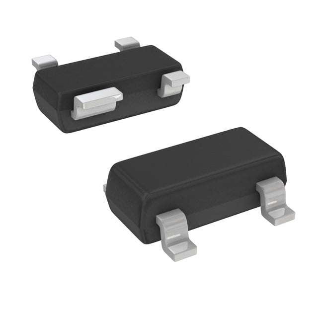
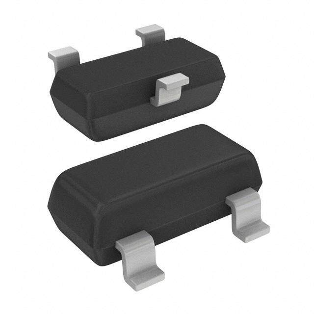
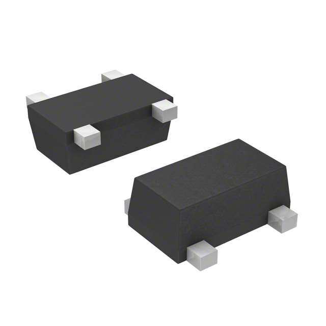
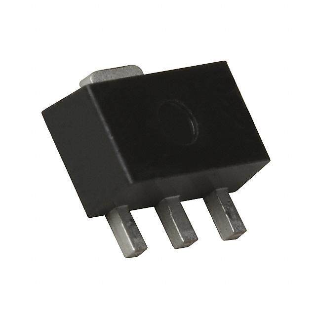
| 产品图片 |
|
| 产品型号 | NE68139-T1-A |
| rohs | 无铅 / 符合限制有害物质指令(RoHS)规范要求 |
| 产品系列 | - |
| 不同 Ic、Vce 时的DC电流增益(hFE)(最小值) | 50 @ 7mA,3V |
| 供应商器件封装 | SOT-143 |
| 其它名称 | NE68139-ADKR |
| 功率-最大值 | 200mW |
| 包装 | Digi-Reel® |
| 噪声系数(dB,不同f时的典型值) | 1.2dB ~ 2dB @ 1GHz |
| 增益 | 13.5dB |
| 安装类型 | 表面贴装 |
| 封装/外壳 | TO-253-4,TO-253AA |
| 晶体管类型 | NPN |
| 标准包装 | 1 |
| 电压-集射极击穿(最大值) | 10V |
| 电流-集电极(Ic)(最大值) | 65mA |
| 频率-跃迁 | 9GHz |


- 商务部:美国ITC正式对集成电路等产品启动337调查
- 曝三星4nm工艺存在良率问题 高通将骁龙8 Gen1或转产台积电
- 太阳诱电将投资9.5亿元在常州建新厂生产MLCC 预计2023年完工
- 英特尔发布欧洲新工厂建设计划 深化IDM 2.0 战略
- 台积电先进制程称霸业界 有大客户加持明年业绩稳了
- 达到5530亿美元!SIA预计今年全球半导体销售额将创下新高
- 英特尔拟将自动驾驶子公司Mobileye上市 估值或超500亿美元
- 三星加码芯片和SET,合并消费电子和移动部门,撤换高东真等 CEO
- 三星电子宣布重大人事变动 还合并消费电子和移动部门
- 海关总署:前11个月进口集成电路产品价值2.52万亿元 增长14.8%


PDF Datasheet 数据手册内容提取
DDAATTAA SSHHEEEETT SILICON TRANSISTOR 2SC4094 NE68139 / JEITA Part No. T MICROWAVE LOW NOISE AMPLIFIER NPN SILICON EPITAXIAL TRANSISTOR 4 PINS MINI MOLD U DESCRIPTION The NE68139 / 2SC4094 is an NPN epitaxial silicon transistor OPACKA(GUnEi tDs:I MmEmN)SIONS designed for use in low-noise and small signal amplifiers from VHF band to UHF band. Low-noise figure, high gain, and high current capability 2.8+-0.03.2 achieve a very wide dynamic range and excellent linearity. This +0.14-0.05 1.5+-0.01.2 +0.14-0.05 0. 0. achieved by direct nitride passivated base surface process (DNP 2 3 pFrEoAceTsUs)R EwShich is a proprietary new fabrication technique. - 2.9±0.2(1.8)0.950.85 (1.9) E 1 4 •• N(cid:1)SF2 =1e (cid:1)12. 2= d1B5 TdYBP T. Y@Pf. =@ 1f .=0 1G.H0 zG, HVzC,E V=C 8E =V ,8 I CV =, I7C =m 2A0 mA +0.10.6-0.05 5(cid:176) 5(cid:176) +0.10.4-0.05 (cid:1)(cid:1) ABCSoOlleLcUtoTr Eto MBaAsXe IVMoUltaMg e RATINVGCBSO (TA =S 25 2C0) V +0.21.1-0.10.8 +0.16-0.06 Collector to Emitter Voltage VCEO 10 V 5(cid:176) o 0.1 5(cid:176) 0.1 Emitter to Base Voltage VEBO 1.5 V 0 t Collector Current IC 65 mA PIN CONNECTIONS Total Power Dissipation APT 200 mW 1. Collector Junction Temperature Tj 150 (cid:2)C 2. Emitter 3. Base Storage Temperature Tstg (cid:3)65 to +150 (cid:2)C 4. Emitter (cid:1)(cid:1) ELECTRICAL CHARACTERISTICS (TA = 25 C) CHARACTERHISTIC SYMBOL MIN. TYP. MAX. UNIT TEST CONDITIONS Collector Cutoff Current ICBO 1.0 (cid:1)A VCB = 10 V, IE = 0 Emitter Cutoff Current IEBO 1.0 (cid:1)A VEB = 1 V, IC = 0 DC Current Gain hFE 50 250 VCE = 8V, IC = 20 mA Gain PBandwidth Product fT 9 GHz VCE = 8 V, IC = 20 mA, f = 1.0 GHz Feed-Back Capacitance Cre 0.25 0.8 pF VCB = 10 V, IE = 0, f = 1.0 MHz Insertion Power Gain (cid:1)S21e(cid:1)2 13 15 dB VCE = 8 V, IC = 20 mA, f = 1.0 GHz Maximum Available Gain MAG 17 dB VCE = 8 V, IC = 20 mA, f = 1.0 GHz Noise Figure NF 1.2 2.0 dB VCE = 8 V, IC = 7 mA, f = 1.0 GHz hFE Classification Class R36/RCF * R37/RCG * R38/RCH * Marking R36 R37 R38 hFE 50 to 100 80 to 160 125 to 250 * Old Specification / New Specification Document No. P10366EJ1V1DS00 (1st edition) Date Published March 1997 N
NE68139 / 2SC4094 TYPICAL CHARACTERISTICS (TA = 25 C) TOTAL POWER DISSIPATION vs. FEED-BACK CAPACITANCE vs. AMBIENT TEMPERATURE COLLECTOR TO BASE VOLTAGE 2.0 T Free air W f = 1.0 GHz m200 ation- ce-pF1.0 p n Dissi acita0.7 U er ap0.5 w100 C o k P c al ba ot d-0.3 T e P-T Fe C-re0.2 O 0 50 100 150 TA-Ambient Temperature-°C 0.1 1 2 3 5 7 10 20 VCB-Collector to Base Voltage-V DC CURRENT GAIN vs. -INSERTION GAIN vs. COLLECTOR CURRENT COLLECTOR CURRENT 200 20 VCE = 8 V E VCE = 8 V f = 1.0 GHz 100 nt Gain ain-dB e G urr 50 S n C o C erti 10 D s h-FE 20 2S|-In21e | A 10 0.5 1 5 10 50 IC-Collector Current-mA 0 1 2 5 10 20 40 IC-Collector Current-mA H GAIN BANDWIDTH PRODUT vs. MAXIMUM AVAILABLE GAIN,INSERTION COLLECTOR CURRENT GAIN vs. FREQUENCY 30 30 VCE = 8 V 20 dB VCE = 8 V Hz ain- MAG IC = 20 mA G P G Gain Bandwidth Product-10753 2S|-Insertion Gain -dB21eMAG-Maximum Available 2100 |S21e|2 f-T 2 | 0 0.1 0.2 0.5 1.0 2.0 1 2 3 5 7 10 20 30 f-Frequency-GHz IC-Collector Current-mA 2
NE68139 / 2SC4094 NOISE FIGURE vs. COLLECTOR CURRENT 7 VCE = 8 V f = 1.0 GHz 6 T B 5 d e- ur g 4 Fi e s oi 3 U N F- N 2 1 0 O 0.5 1 5 10 50 70 IC-Collector Current-mA S-PARAMETER VCE = 8.0 V, IC = 5.0 mA, ZO = 50 - f (MHz) S11 S11 S21 S21 S12 S12 S22 S22 200 0.774 47.8 12.689 146.5 0.031 65.4 0.882 19.1 E 400 0.631 88.8 9.952 119.4 0.048 53.4 0.723 29.5 600 0.523 120.9 7.813 100.9 0.058 46.2 0.611 33.4 800 0.460 145.1 5.966 87.6 0.067 43.9 0.564 34.5 1000 0.426 166.6 4.841 76.7 0.074 43.8 0.515 37.6 1200 0.416 178.2 4.065 68.8 0.083 43.5 0.488 39.6 S 1400 0.417 163.0 3.413 60.7 0.087 41.2 0.459 44.1 1600 0.430 152.1 3.035 54.1 0.098 42.8 0.443 45.9 1800 0.443 142.1 2.659 48.0 0.105 40.1 0.428 51.1 2000 0.458 136.5 2.482 44.3 0.114 43.0 0.414 53.5 A VCE = 8.0 V, IC = 20.0 mA, ZO = 50 f (MHz) S11 S11 S21 S21 S12 S12 S22 S22 200 0.461 89.8 23.331 121.6 0.021 60.7 0.665 27.7 400 0.H364 135.8 13.501 99.2 0.033 61.2 0.511 30.5 600 0.338 163.4 9.535 86.4 0.046 61.5 0.448 29.5 800 0.330 177.9 7.083 77.5 0.056 62.1 0.430 29.5 1000 0.334 163.2 5.604 69.3 0.070 60.0 0.402 32.5 1200 0.344 153.9 4.722 63.5 0.084 60.4 0.385 34.8 1400 0.359 143.1 3.982 56.8 0.091 54.9 0.362 39.5 P 1600 0.383 136.1 3.517 51.1 0.104 54.5 0.350 42.1 1800 0.401 128.3 3.094 45.6 0.116 49.9 0.337 47.4 2000 0.419 124.7 2.882 42.7 0.127 50.8 0.323 50.5 3
NE68139 / 2SC4094 S-PARAMETER S11e, S22e-FREQUENCY CONDITION VCE = 8 V, IC = 20/5 mA, freq. = 0.2 to 2 GHz (Step 200 MHz) S21e-FREQUENCY WAVELENG0T904H..00S1TO840W..00A2R0D100..409G740E2..00ND.00A.O40EL38DRRAWAOITNCCEOLO3FETEFFRTC060IF.OEOS.NE40H40TL.IRGT7.NNG00DANE40GE64RL1−0EE00E.V10.S0A45W..64001..000255501.100−.05.20.045440.3.T000.1.N6P000EO.6N040SIO1.3T1.IP404−VME 0O4RC3E EA40CC4.NT.7. 0AA00(0 ).+ T N0X0 J–4C7 .–C0 J–X .A− –E–043EZ––0.2)1CSRO3O–1Z(O3 − E 2M V0 PI4 10T5.O8A..00G1N.00005EE.8.eNN04T0.30221112−0496.0.00.0.0006..9400.41 00010714.200.0.710.511.1.0−.04 0R00GEIACC0.6TH9 A8010.0.80I3N=.01C.1.Cz1300.70.E10 091 5 =0C−0 0.8.O99 .0 ( M m– 822 0P0–RZ3O–1.O.0.91–30N..A0)02E82N0 1.001.0.19Tm9 0−G2020..030470.2.00A2..14.3.1.200H341.6..0.0740.03.6060.z.086I1.402..18.01.C020.88E.0084800 06.01.1−.1.3=031.6.1011..60.040. 221.84.11. 0402.05G0.51307 .I31.570m0C.5H−06 .1-1.6=Az06.0 314.5.3.041380.061.16.08 0006m−00.4.0722..3001A.33S.103.7015.05000528.−3e10.22-.013S.F800.033.4092R.0034110.210−01.e1E30.9.4040.0.020Q30230.0006.3050.−00.23U..00100.1222.102900520200O5E−0020 9.0222..1G012201.080−N003.2028.7.022H.2004.2C2.6052.007.22.3z00Y6.22.4052.0 U T CONDITION VCE = 8 V CONDITION VCE = 8 V IC = 20/5 mA IC = 20/5 mA freq. = 0.2 to 2 GHz (Step 200 MHz) freq. = 0.2 to 2 GHz (Step 200 MHz) 90° S 90° 120° 60° 120° 60° IC = 20 mA 0.2 GHz 150° AS21e 30° 150° IC = 20 mA 2GHz 30° S12e IC = 5 mA IC = 5 mA 2GHz 0.2 GHz 180° 0°180° 0° 0 4 8 12 16 20 0 0.04 0.08 0.12 0.16 0.2 H −150° −30° −150° −30° P −120° −60° −120° −60° −90° −90° 4
NOTICE 1. Descriptions of circuits, software and other related information in this document are provided only to illustrate the operation of semiconductor products and application examples. You are fully responsible for the incorporation of these circuits, software, and information in the design of your equipment. California Eastern Laboratories and Renesas Electronics assumes no responsibility for any losses incurred by you or third parties arising from the use of these circuits, software, or information. T 2. California Eastern Laboratories has used reasonable care in preparing the information included in this document, but California Eastern Laboratories does not warrant that such information is error free. California Eastern Laboratories and Renesas Electronics assumes no liability whatsoever for any damages incurred by you resulting from errors in or omissions from the information included herein. 3. California Eastern Laboratories and Renesas Electronics do not assume any liability for infringement of patents, copyrights, or other intellectual property rights of third parties by or arising from the use of Renesas Electronics products or technical information described in this document. No license, express, U implied or otherwise, is granted hereby under any patents, copyrights or other intellectual property rights of California Eastern Laboratories or Renesas Electronics or others. 4. You should not alter, modify, copy, or otherwise misappropriate any Renesas Electronics product, whether in whole or in part. California Eastern Laboratories and Renesas Electronics assume no responsibility for any losses incurred by you or third parties arising from such alteration, modification, copy or otherwise misappropriation of Renesas Electronics product. 5. Renesas Electronics products are classified according to the following two quality grades: “Standard” and “High Quality”. The recommended applications for each Renesas Electronics product depends on the product’s quality grade, as indicated below. “Standard”: Computers; office equipment; communications O equipment; test and measurement equipment; audio and visual equipment; home electronic appliances; machine tools; personal electronic equipment; and industrial robots etc. “High Quality”: Transportation equipment (automobiles, trains, ships, etc.); traffic control systems; anti-disaster systems; anti-crime systems; and safety equipment etc. Renesas Electronics products are neither intended nor authorized for use in products or systems that may pose a direct threat to human life or bodily injury (artificial life support devices or systems, surgical implantations etc.), or may cause serious property damages (nuclear reactor control systems, military equipment etc.). You must check the quality grade of each Renesas Electronics product before using it in a particular application. You may not use any Renesas Electronics product for any application for which it is not intended. California Eastern Laboratories and Renesas Electronics shall not be in any way liable for any damages or losses incurred by you or third parties arising from the use of any Renesas Electronics product for which the product is not intended by California Eastern Laboratories or Renesas Elec-tronics. 6. You should use the Renesas Electronics products described in this document within the range specified by California Eastern Laboratories, especially with respect to the maximum rating, operating supply voltage range, movement power voltage range, heat radiation characteristics, installation and other product characteristics. California Eastern Laboratories shall have no liability for malfunEctions or damages arising out of the use of Renesas Electronics products beyond such specified ranges. 7. Although Renesas Electronics endeavors to improve the quality and reliability of its products, semiconductor products have specific characteristics such as the occurrence of failure at a certain rate and malfunctions under certain use conditions. Further, Renesas Electronics products are not subject to radiation resistance design. Please be sure to implement safety measures to guard them against the possibility of physical injury, and injury or damage caused by fire in the event of the failure of a Renesas Electronics product, such as safety design for hardware and software including but not limited to redundancy, fire control and malfunction prevention, appropriate treatment for aging degradation or any other appropriate measures. Because the evaluation of S microcomputer software alone is very difficult, please evaluate the safety of the final products or systems manufactured by you. 8. Please contact a California Eastern Laboratories sales office for details as to environmental matters such as the environmental compatibility of each Renesas Electronics product. Please use Renesas Electronics products in compliance with all applicable laws and regulations that regulate the inclusion or use of controlled substances, including without limitation, the EU RoHS Directive. California Eastern Laboratories and Renesas Electronics assume no liability for damages or losses occurring as a result of your noncompliance with applicable laws and regulations. 9. Renesas Electronics products and technology may not be used for or incorporated into any products or systems whose manufacture, use, or sale is prohibited under any applicable domestic or foreign laws oAr regulations. You should not use Renesas Electronics products or technology described in this document for any purpose relating to military applications or use by the military, including but not limited to the development of weapons of mass destruction. When exporting the Renesas Electronics products or technology described in this document, you should comply with the applicable export control laws and regulations and follow the procedures required by such laws and regulations. 10. It is the responsibility of the buyer or distributor of California Eastern Laboratories, who distributes, disposes of, or otherwise places the Renesas Electronics product with a third party, to notify such third party in advance of the contents and conditions set forth in this document, California Eastern Laboratories and Renesas Electronics assume no responsibility for any losses incurred by you or third parties as a result of unauthorized use of Renesas Electronics products. H 11. This document may not be reproduced or duplicated in any form, in whole or in part, without prior written consent of California Eastern Laboratories. 12. Please contact a California Eastern Laboratories sales office if you have any questions regarding the information contained in this document or Renesas Electronics products, or if you have any other inquiries. NOTE 1: “Renesas Electronics” as used in this document means Renesas Electronics Corporation and also includes its majority-owned subsidiaries. NOTE 2: “Renesas Electronics product(s)” means any product developed or manufactured by or for Renesas Electronics. NOTE 3: Products and product information are subject to change without notice. P CEL Headquarters • 4590 Patrick Henry Drive, Santa Clara, CA 95054 • Phone (408) 919-2500 • www.cel.com For a complete list of sales offices, representatives and distributors, Please visit our website: www.cel.com/contactus