ICGOO在线商城 > 分立半导体产品 > 晶体管 - 双极 (BJT) - 射频 > BFR92AW,115
 Datasheet下载
- 型号: BFR92AW,115
- 制造商: NXP Semiconductors
- 库位|库存: xxxx|xxxx
- 要求:
| 数量阶梯 | 香港交货 | 国内含税 |
| +xxxx | $xxxx | ¥xxxx |
查看当月历史价格
查看今年历史价格
BFR92AW,115产品简介:
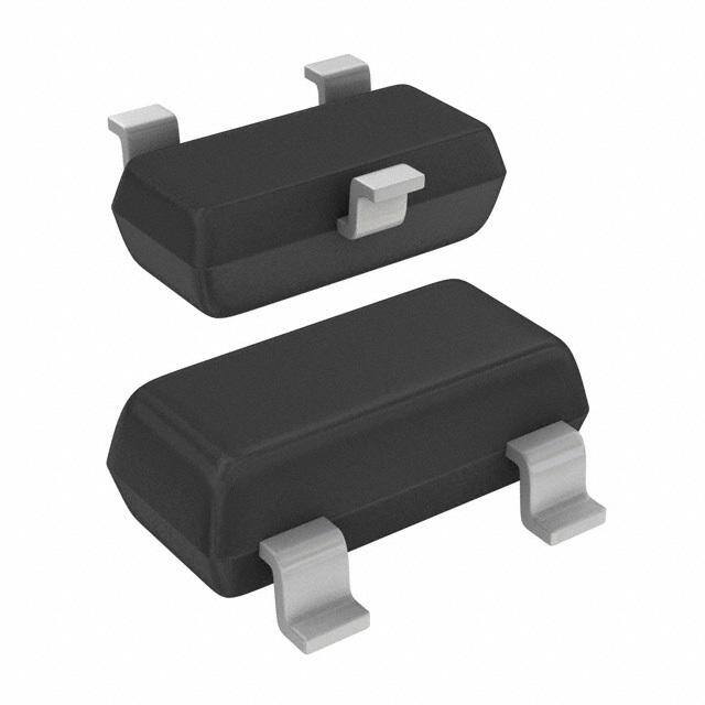
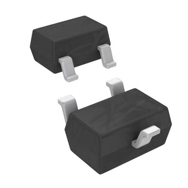
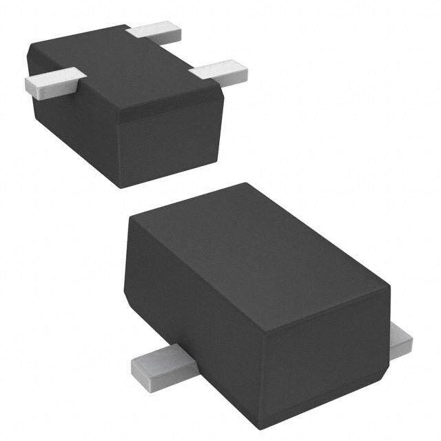
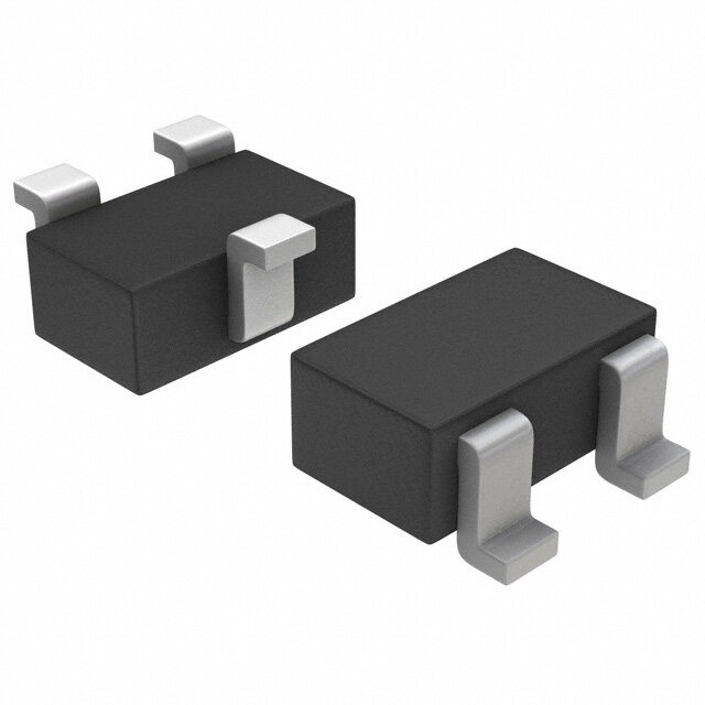
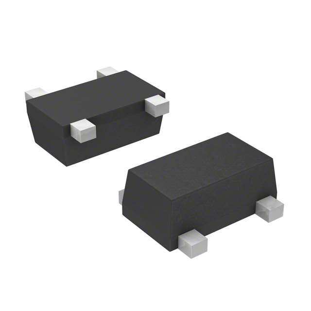
ICGOO电子元器件商城为您提供BFR92AW,115由NXP Semiconductors设计生产,在icgoo商城现货销售,并且可以通过原厂、代理商等渠道进行代购。 BFR92AW,115价格参考。NXP SemiconductorsBFR92AW,115封装/规格:晶体管 - 双极 (BJT) - 射频, RF Transistor NPN 15V 25mA 5GHz 300mW Surface Mount SOT-323-3。您可以下载BFR92AW,115参考资料、Datasheet数据手册功能说明书,资料中有BFR92AW,115 详细功能的应用电路图电压和使用方法及教程。
NXP USA Inc. 生产的 BFR92AW,115 是一款高频硅 NPN 双极结型晶体管(BJT),属于射频(RF)晶体管类别,广泛应用于高频小信号放大和开关场景。该器件具有高增益、低噪声和优异的高频性能,典型应用频率可达数百兆赫兹至数吉赫兹范围。

BFR92AW,115 常用于无线通信系统中的射频前端模块,如 FM 收音机、对讲机、无线麦克风、遥控设备和短距离无线传输系统(如 RFID 和 ISM 频段设备)。由于其良好的线性度和稳定性,也适用于电视调谐器、卫星接收器和有线电视(CATV)设备中的信号放大。

此外,该晶体管在消费类电子产品中应用广泛,例如智能手机周边电路、无线局域网(WLAN)模块和蓝牙设备中的低噪声放大器(LNA)或驱动放大器。其 SOT-23 小型封装适合高密度贴装,有利于缩小产品体积,提升集成度。

BFR92AW,115 还具备良好的温度稳定性和可靠性,适合工业控制、汽车电子中的射频传感与通信模块。总体而言,该器件适用于需要高频响应、低功耗和高可靠性的中小信号射频放大场景,是模拟和混合信号射频设计中的常用元件。
| 参数 | 数值 |
| 产品目录 | |
| 描述 | TRANS NPN 15V 5GHZ SOT323射频双极晶体管 NPN 15V 5GHZ |
| 产品分类 | RF 晶体管 (BJT)分离式半导体 |
| 品牌 | NXP Semiconductors |
| 产品手册 | |
| 产品图片 |
|
| rohs | 符合RoHS无铅 / 符合限制有害物质指令(RoHS)规范要求 |
| 产品系列 | 晶体管,晶体管射频,射频双极晶体管,NXP Semiconductors BFR92AW,115- |
| 数据手册 | |
| 产品型号 | BFR92AW,115 |
| PCN封装 | |
| 不同 Ic、Vce 时的DC电流增益(hFE)(最小值) | 65 @ 15mA,10V |
| 产品目录页面 | |
| 产品种类 | 射频双极晶体管 |
| 供应商器件封装 | SOT-323 |
| 其它名称 | 568-1989-6 |
| 功率-最大值 | 300mW |
| 功率耗散 | 300 mW |
| 包装 | Digi-Reel® |
| 发射极-基极电压VEBO | 2 V |
| 商标 | NXP Semiconductors |
| 噪声系数(dB,不同f时的典型值) | 2dB ~ 3dB @ 1GHz ~ 2GHz |
| 增益 | - |
| 安装类型 | 表面贴装 |
| 安装风格 | SMD/SMT |
| 封装 | Reel |
| 封装/外壳 | SC-70,SOT-323 |
| 封装/箱体 | SOT-323 |
| 工厂包装数量 | 3000 |
| 技术 | Silicon |
| 晶体管极性 | NPN |
| 晶体管类型 | Bipolar |
| 最大工作温度 | + 150 C |
| 最大工作频率 | 5000 MHz |
| 最大直流电集电极电流 | 0.025 A |
| 最小工作温度 | - 65 C |
| 标准包装 | 1 |
| 电压-集射极击穿(最大值) | 15V |
| 电流-集电极(Ic)(最大值) | 25mA |
| 类型 | RF Bipolar Small Signal |
| 配置 | Single |
| 集电极—发射极最大电压VCEO | 15 V |
| 集电极连续电流 | 0.025 A |
| 零件号别名 | BFR92AW T/R |
| 频率 | 5000 MHz |
| 频率-跃迁 | 5GHz |


- 商务部:美国ITC正式对集成电路等产品启动337调查
- 曝三星4nm工艺存在良率问题 高通将骁龙8 Gen1或转产台积电
- 太阳诱电将投资9.5亿元在常州建新厂生产MLCC 预计2023年完工
- 英特尔发布欧洲新工厂建设计划 深化IDM 2.0 战略
- 台积电先进制程称霸业界 有大客户加持明年业绩稳了
- 达到5530亿美元!SIA预计今年全球半导体销售额将创下新高
- 英特尔拟将自动驾驶子公司Mobileye上市 估值或超500亿美元
- 三星加码芯片和SET,合并消费电子和移动部门,撤换高东真等 CEO
- 三星电子宣布重大人事变动 还合并消费电子和移动部门
- 海关总署:前11个月进口集成电路产品价值2.52万亿元 增长14.8%


PDF Datasheet 数据手册内容提取
BFR92AW NPN 5 GHz wideband transistor Rev. 03 — 12 March 2008 Product data sheet IMPORTANT NOTICE Dear customer, As from October 1st, 2006 Philips Semiconductors has a new trade name -NXPSemiconductors,whichwillbeusedinfuturedatasheetstogetherwithnewcontact details. IndatasheetswherethepreviousPhilipsreferencesremain,pleaseusethenewlinksas shown below. http://www.philips.semiconductors.com use http://www.nxp.com http://www.semiconductors.philips.com use http://www.nxp.com (Internet) sales.addresses@www.semiconductors.philips.com use salesaddresses@nxp.com (email) The copyright notice at the bottom of each page (or elsewhere in the document, depending on the version) - © Koninklijke Philips Electronics N.V. (year). All rights reserved - is replaced with: - © NXP B.V. (year). All rights reserved. - If you have any questions related to the data sheet, please contact our nearest sales office via e-mail or phone (details via salesaddresses@nxp.com). Thank you for your cooperation and understanding, NXP Semiconductors
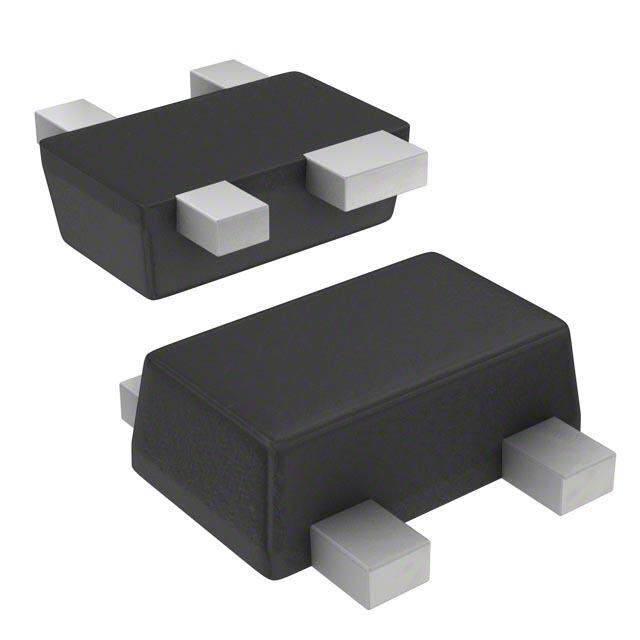
NXP Semiconductors Product specification NPN 5 GHz wideband transistor BFR92AW FEATURES DESCRIPTION • High power gain Silicon NPN transistor encapsulated handbook, 2 columns 3 • Gold metallization ensures in a plastic SOT323 (S-mini) package. The BFR92AW uses the same crystal excellent reliability as the SOT23 version, BFR92A. • SOT323 (S-mini) package. PINNING APPLICATIONS 1 2 PIN DESCRIPTION It is designed for use in RF amplifiers, Top view MBC870 mixers and oscillators with signal 1 base Marking code: P2. frequencies up to 1GHz. 2 emitter Fig.1 SOT323 3 collector QUICK REFERENCE DATA SYMBOL PARAMETER CONDITIONS MIN. TYP. MAX. UNIT V collector-base voltage open emitter - - 20 V CBO V collector-emitter voltage open base - - 15 V CEO I collector current (DC) - - 25 mA C P total power dissipation up to T =93(cid:176) C; note1 - - 300 mW tot s hFE current gain IC=15mA; VCE=10V 65 90 135 C feedback capacitance I =0; V =10V; f=1MHz; - 0.35 - pF re C CE T =25(cid:176) C amb f transition frequency I =15mA; V =10V; f=500MHz 3.5 5 - GHz T C CE G maximum unilateral power I =15mA; V =10V; f=1GHz; - 14 - dB UM C CE gain T =25(cid:176) C amb I =15mA; V =10V; f=2GHz; - 8 - dB C CE T =25(cid:176) C amb F noise figure I =5mA; V =10V; f=1GHz; - 2 - dB C CE G =G s opt T junction temperature - - 150 (cid:176) C j Note 1. T is the temperature at the soldering point of the collector pin. s Rev. 03 - 12 March 2008 2 of 13
NXP Semiconductors Product specification NPN 5 GHz wideband transistor BFR92AW LIMITING VALUES In accordance with the Absolute Maximum System (IEC 134). SYMBOL PARAMETER CONDITIONS MIN. MAX. UNIT V collector-base voltage open emitter - 20 V CBO V collector-emitter voltage open base - 15 V CEO V emitter-base voltage open collector - 2 V EBO I collector current (DC) - 25 mA C P total power dissipation up to T =93(cid:176) C; seeFig.2; note1 - 300 mW tot s T storage temperature - 65 +150 (cid:176) C stg T junction temperature - 150 (cid:176) C j THERMAL CHARACTERISTICS SYMBOL PARAMETER CONDITIONS VALUE UNIT R thermal resistance from junction to up to T =93(cid:176) C; note1 190 K/W thj-s s soldering point Note to the Limiting values and Thermal characteristics 1. T is the temperature at the soldering point of the collector pin. s MLB540 400 Ptot (mW) 300 200 100 0 0 50 100 150 200 T s ( o C) Fig.2 Power derating curve Rev. 03 - 12 March 2008 3 of 13
NXP Semiconductors Product specification NPN 5 GHz wideband transistor BFR92AW CHARACTERISTICS T =25(cid:176) C (unless otherwise specified). j SYMBOL PARAMETER CONDITIONS MIN. TYP. MAX. UNIT I collector leakage current I =0; V =10V - - 50 nA CBO E CB hFE DC current gain IC=15mA; VCE=10V 65 90 135 C collector capacitance I =i =0; V =10V; f=1MHz - 0.6 - pF c E e CB C emitter capacitance I =i =0; V =0.5V; f=1MHz - 0.9 - pF e C c EB C feedback capacitance I =0; V =10V; f=1MHz - 0.35 - pF re C CE f transition frequency I =15mA; V =10V; f=500MHz 3.5 5 - GHz T C CE G maximum unilateral power I =15mA; V =10V; - 14 - dB UM C CE gain; note1 f=1GHz; T =25(cid:176) C amb I =15mA; V =10V; - 8 - dB C CE f=2GHz; T =25(cid:176) C amb F noise figure I =5mA; V =10V; - 2 - dB C CE f=1GHz;G =G s opt I =5mA; V =10V; - 3 - dB C CE f=2GHz;G =G s opt Note s 2 1. G is the maximum unilateral power gain, assuming s is zero and G = 10 log-----------------------------2--1----------------------------- dB. UM 12 UM (1– s 2) (1– s 2) 11 22 Rev. 03 - 12 March 2008 4 of 13
NXP Semiconductors Product specification NPN 5 GHz wideband transistor BFR92AW MGC883 MCD074 1.0 120 handbook, halfpage Cre (pF) hFE 0.8 80 0.6 0.4 40 0.2 0 0 0 4 8 12 16 20 0 10 20 30 I C (mA) V C B (V) VCE=10V. IC=0; f=1MHz. Fig.3 DC current gain as a function of collector Fig.4 Feedback capacitance as a function of current; typical values. collector-base voltage; typical values. MGC884 6 handbook, halfpage f T (GHz) 4 2 0 1 10 I C (mA) 102 VCE=5V; f=500MHz; Tamb=25(cid:176)C. Fig.5 Transition frequency as a function of collector current; typical values. Rev. 03 - 12 March 2008 5 of 13
NXP Semiconductors Product specification NPN 5 GHz wideband transistor BFR92AW MGC885 MGC886 30 30 handbook, halfpage handbook, halfpage gain gain (dB) (dB) MSG 20 20 G UM MSG G UM 10 10 0 0 0 5 10 15 20 0 5 10 15 20 I C (mA) I C (mA) VCE=10V;f=500MHz. VCE=10V;f=1GHz. Fig.6 Gain as a function of collector current; Fig.7 Gain as a function of collector current; typical values. typical values. MGC887 MGC888 50 50 handbook, halfpage handbook, halfpage gain gain (dB) GUM (dB) GUM 40 40 MSG MSG 30 30 20 20 10 10 Gmax Gmax 0 0 10 102 103 104 10 102 103 104 f (MHz) f (MHz) VCE=10V;IC=5mA. VCE=10V;IC=15mA. Fig.8 Gain as a function of frequency; Fig.9 Gain as a function of frequency; typical values. typical values. Rev. 03 - 12 March 2008 6 of 13
NXP Semiconductors Product specification NPN 5 GHz wideband transistor BFR92AW MGC889 MGC890 6 6 handbook, halfpage handbook, halfpage F F (dB) (dB) f = 2 GHz 4 4 I = 15 mA C 1 GHz 10 mA 500 MHz 5 mA 2 2 0 0 1 10 I C (mA) 102 102 103 f (MHz) 104 VCE=10V. VCE=10V. Fig.10 Minimum noise figure as a function of Fig.11 Minimum noise figure as a function of collector current; typical values. frequency; typical values. 90o handbook, full pagewidth 1.0 1 135o F = 4 dB 45o 0.8 0.5 2 F = 3 dB 0.6 F = 2 dB 0.4 0.2 5 F m in = 1.6 dB 0.2 G opt 0.2 0.5 1 2 5 180o 0 0o 0 0.2 5 0.5 2 135o 45o 1 MGC891 1.0 90o f=500MHz; VCE=10V; IC=5mA; Zo=50W . Fig.12 Common emitter noise figure circles; typical values. Rev. 03 - 12 March 2008 7 of 13
NXP Semiconductors Product specification NPN 5 GHz wideband transistor BFR92AW 90o handbook, full pagewidth 1.0 1 135o 45o 0.8 0.5 2 0.6 (4) (2) (3) 0.4 0.2 5 (5) (1) 0.2 (6) 0.2 0.5 1 2 5 180o 0 0o 0 (7) (8) (1) G opt; Fmin=2.1dB. 0.2 5 (2) F=2.5dB. (3) F=3dB. (4) F=4dB. 0.5 2 (5) G ms;Gmax=15.7dB. 135o 45o (6) G=15dB. 1 (7) G=14dB. MGC892 1.0 (8) G=13dB. 90o f=1GHz; VCE=10V; IC=5mA; Zo=50W. Fig.13 Common emitter noise figure circles; typical values. 90o handbook, full pagewidth 1.0 1 135o 45o 0.8 0.5 2 (4) 0.6 (3) (2) 0.4 0.2 5 0.2 (1) 0.2 0.5 1 2 5 180o 0 0o 0 (5) 0.2 5 (6) (1) G opt; Fmin=3dB. (7) (2) F=3.5dB. (3) F=4dB. (8) 0.5 2 (4) F=5dB. 135o 45o (5) G ms;Gmax=9.1dB. 1 (6) G=8dB. MGC893 1.0 (7) G=7dB. 90o (8) G=6dB. f=2GHz; VCE=10V; IC=5mA; Zo=50W. Fig.14 Common emitter noise figure circles; typical values. Rev. 03 - 12 March 2008 8 of 13
NXP Semiconductors Product specification NPN 5 GHz wideband transistor BFR92AW 90o handbook, full pagewidth 1.0 1 135o 45o 0.8 0.5 2 0.6 0.4 0.2 5 3 GHz 0.2 0.2 0.5 1 2 5 180o 0 0o 0 40 MHz 0.2 5 0.5 2 135o 45o 1 MGC894 1.0 90o VCE=10V; IC=15mA; Zo=50W . Fig.15 Common emitter input reflection coefficient (s ); typical values. 11 90o handbook, full pagewidth 135o 45o 40 MHz 180o 3 GHz 0o 50 40 30 20 10 135o 45o 90o MGC895 VCE=10V; IC=15mA. Fig.16 Common emitter forward transmission coefficient (s ); typical values. 21 Rev. 03 - 12 March 2008 9 of 13
NXP Semiconductors Product specification NPN 5 GHz wideband transistor BFR92AW handbook, full pagewidth 90o 3 GHz 135o 45o 40 MHz 180o 0o 0.25 0.20 0.15 0.10 0.05 135o 45o 90o MGC896 VCE=10V; IC=15mA. Fig.17 Common emitter reverse transmission coefficient (s ); typical values. 12 90o handbook, full pagewidth 1.0 1 135o 45o 0.8 0.5 2 0.6 0.4 0.2 5 0.2 0.2 0.5 1 2 5 180o 0 0o 0 40 MHz 0.2 3 GHz 5 0.5 2 135o 45o 1 MGC897 1.0 90o VCE=10V; IC=15mA; Zo=50W . Fig.18 Common emitter output reflection coefficient (s ); typical values. 22 Rev. 03 - 12 March 2008 10 of 13
NXP Semiconductors Product specification NPN 5 GHz wideband transistor BFR92AW PACKAGE OUTLINE 2.2 1.35 A B handbook, full pagewidth 1.8 1.15 X 0.25 0.10 2.2 0.2 M B 2.0 3 0.2 1.0 1.1 0.8 0.1 max 0.0 1 0.40 2 0.30 0.2 M A 0.3 0.65 0.1 detail X MBC871 1.3 Dimensions in mm. Fig.19 SOT323. Rev. 03 - 12 March 2008 11 of 13
BFR92AW NXP Semiconductors NPN 5 GHz wideband transistor Legal information Data sheet status Document status[1][2] Product status[3] Definition Objective [short] data sheet Development This document contains data from the objective specification for product development. Preliminary [short] data sheet Qualification This document contains data from the preliminary specification. Product [short] data sheet Production This document contains the product specification. [1] Please consult the most recently issued document before initiating or completing a design. [2] The term ‘short data sheet’ is explained in section “Definitions”. [3] Theproductstatusofdevice(s)describedinthisdocumentmayhavechangedsincethisdocumentwaspublishedandmaydifferincaseofmultipledevices.Thelatestproductstatus information is available on the Internet at URLhttp://www.nxp.com. Definitions damage. NXP Semiconductors accepts no liability for inclusion and/or use of NXP Semiconductors products in such equipment or applications and therefore such inclusion and/or use is at the customer’s own risk. Draft —The document is a draft version only. The content is still under internal review and subject to formal approval, which may result in Applications —Applications that are described herein for any of these modifications or additions. NXP Semiconductors does not give any products are for illustrative purposes only. NXP Semiconductors makes no representations or warranties as to the accuracy or completeness of representation or warranty that such applications will be suitable for the informationincludedhereinandshallhavenoliabilityfortheconsequencesof specified use without further testing or modification. use of such information. Limiting values —Stress above one or more limiting values (as defined in Short data sheet —A short data sheet is an extract from a full data sheet theAbsoluteMaximumRatingsSystemofIEC60134)maycausepermanent withthesameproducttypenumber(s)andtitle.Ashortdatasheetisintended damagetothedevice.Limitingvaluesarestressratingsonlyandoperationof forquickreferenceonlyandshouldnotbereliedupontocontaindetailedand the device at these or any other conditions above those given in the full information. For detailed and full information see the relevant full data Characteristics sections of this document is not implied. Exposure to limiting sheet, which is available on request via the local NXP Semiconductors sales values for extended periods may affect device reliability. office. In case of any inconsistency or conflict with the short data sheet, the Terms and conditions of sale —NXP Semiconductors products are sold full data sheet shall prevail. subjecttothegeneraltermsandconditionsofcommercialsale,aspublished athttp://www.nxp.com/profile/terms, including those pertaining to warranty, Disclaimers intellectual property rights infringement and limitation of liability, unless explicitly otherwise agreed to in writing by NXP Semiconductors. In case of any inconsistency or conflict between information in this document and such General —Information in this document is believed to be accurate and terms and conditions, the latter will prevail. reliable.However,NXPSemiconductorsdoesnotgiveanyrepresentationsor No offer to sell or license —Nothing in this document may be interpreted warranties,expressedorimplied,astotheaccuracyorcompletenessofsuch or construed as an offer to sell products that is open for acceptance or the information and shall have no liability for the consequences of use of such grant,conveyanceorimplicationofanylicenseunderanycopyrights,patents information. or other industrial or intellectual property rights. Right to make changes —NXPSemiconductorsreservestherighttomake Quick reference data —The Quick reference data is an extract of the changes to information published in this document, including without product data given in the Limiting values and Characteristics sections of this limitation specifications and product descriptions, at any time and without document, and as such is not complete, exhaustive or legally binding. notice.Thisdocumentsupersedesandreplacesallinformationsuppliedprior to the publication hereof. Suitability for use —NXP Semiconductors products are not designed, Trademarks authorized or warranted to be suitable for use in medical, military, aircraft, space or life support equipment, nor in applications where failure or Notice:Allreferencedbrands,productnames,servicenamesandtrademarks malfunction of an NXP Semiconductors product can reasonably be expected are the property of their respective owners. to result in personal injury, death or severe property or environmental Contact information For more information, please visit:http://www.nxp.com For sales office addresses, please send an email to:salesaddresses@nxp.com Rev. 03 - 12 March 2008 12 of 13
BFR92AW NXP Semiconductors NPN 5 GHz wideband transistor Revision history Revision history Document ID Release date Data sheet status Change notice Supersedes BFR92AW_N_3 20080312 Product data sheet - BFR92AW_2 Modifications: • Quick reference data and Characteristics Table; DC current gain value changed BFR92AW_2 19950918 Product specification - BFR92AW_1 BFR92AW_1 19921001 - - - Pleasebeawarethatimportantnoticesconcerningthisdocumentandtheproduct(s) described herein, have been included in section ‘Legal information’. © NXP B.V. 2008. All rights reserved. For more information, please visit: http://www.nxp.com For sales office addresses, please send an email to: salesaddresses@nxp.com Date of release: 12 March 2008 Document identifier: BFR92AW_N_3