ICGOO在线商城 > 分立半导体产品 > 晶体管 - FET,MOSFET - 单 > MMBF2201NT1G
 Datasheet下载
- 型号: MMBF2201NT1G
- 制造商: ON Semiconductor
- 库位|库存: xxxx|xxxx
- 要求:
| 数量阶梯 | 香港交货 | 国内含税 |
| +xxxx | $xxxx | ¥xxxx |
查看当月历史价格
查看今年历史价格
MMBF2201NT1G产品简介:
ICGOO电子元器件商城为您提供MMBF2201NT1G由ON Semiconductor设计生产,在icgoo商城现货销售,并且可以通过原厂、代理商等渠道进行代购。 MMBF2201NT1G价格参考。ON SemiconductorMMBF2201NT1G封装/规格:晶体管 - FET,MOSFET - 单, 表面贴装 N 沟道 20V 300mA(Ta) 150mW(Ta) SC-70-3(SOT323)。您可以下载MMBF2201NT1G参考资料、Datasheet数据手册功能说明书,资料中有MMBF2201NT1G 详细功能的应用电路图电压和使用方法及教程。
MMBF2201NT1G 是一款由 ON Semiconductor 生产的 N 沟道增强型 MOSFET(金属氧化物场效应晶体管)。它属于小信号 MOSFET,适用于多种低功率和中等功率的应用场景。以下是该型号的主要应用场景:

 1. 电源管理
   MMBF2201NT1G 常用于电源管理系统中的开关应用。它可以作为开关元件用于降压、升压或反相转换器中,帮助调节电压和电流。其低导通电阻特性有助于减少功率损耗,提高效率。

 2. 信号切换
   在音频设备、通信设备和其他需要信号切换的电路中,MMBF2201NT1G 可以用作模拟开关。它能够快速响应控制信号,实现信号路径的切换,同时保持较低的噪声和失真。

 3. 负载控制
   该器件可用于控制小型电机、LED 灯或其他低功耗负载。通过改变栅极电压,可以精确控制负载的开启和关闭,适用于智能家居、消费电子等领域。

 4. 保护电路
   MMBF2201NT1G 还可以用于设计过流保护、短路保护和反向电池保护电路。其内置的体二极管可以在反向电压条件下提供一定的保护功能,防止电路损坏。

 5. 便携式设备
   由于其低功耗和小封装尺寸,MMBF2201NT1G 广泛应用于便携式设备如智能手机、平板电脑、可穿戴设备等。这些设备对空间和功耗要求严格,MOSFET 的高效性能使其成为理想选择。

 6. 汽车电子
   在汽车电子系统中,MMBF2201NT1G 可用于车身控制模块、传感器接口、车载娱乐系统等。它能够承受较宽的工作温度范围,并具备良好的抗干扰能力。

总之,MMBF2201NT1G 以其紧凑的封装、低导通电阻和高可靠性,广泛应用于各种需要高效开关和信号处理的领域。
| 参数 | 数值 |
| 产品目录 | |
| ChannelMode | Enhancement |
| 描述 | MOSFET N-CH 20V 300MA SOT-323MOSFET 20V 300mA N-Channel |
| 产品分类 | FET - 单分离式半导体 |
| FET功能 | 逻辑电平门 |
| FET类型 | MOSFET N 通道,金属氧化物 |
| Id-ContinuousDrainCurrent | 300 mA |
| Id-连续漏极电流 | 300 mA |
| 品牌 | ON Semiconductor |
| 产品手册 | |
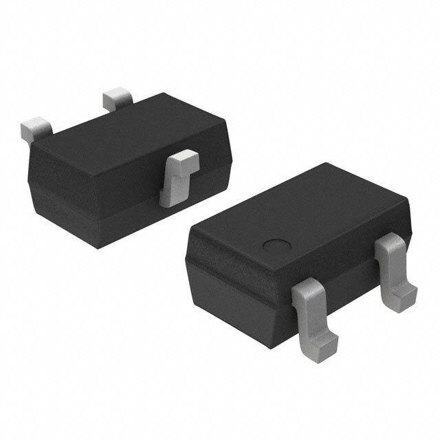
| 产品图片 |
|
| rohs | 符合RoHS无铅 / 符合限制有害物质指令(RoHS)规范要求 |
| 产品系列 | 晶体管,MOSFET,ON Semiconductor MMBF2201NT1G- |
| 数据手册 | |
| 产品型号 | MMBF2201NT1G |
| PCN设计/规格 | |
| Pd-PowerDissipation | 0.15 W |
| Pd-功率耗散 | 150 mW |
| RdsOn-Drain-SourceResistance | 1 Ohms |
| RdsOn-漏源导通电阻 | 1 Ohms |
| Vds-Drain-SourceBreakdownVoltage | 20 V |
| Vds-漏源极击穿电压 | 20 V |
| Vgs-Gate-SourceBreakdownVoltage | +/- 20 V |
| Vgs-栅源极击穿电压 | 20 V |
| 上升时间 | 2.5 ns |
| 下降时间 | 2.5 ns |
| 不同Id时的Vgs(th)(最大值) | 2.4V @ 250µA |
| 不同Vds时的输入电容(Ciss) | 45pF @ 5V |
| 不同Vgs时的栅极电荷(Qg) | - |
| 不同 Id、Vgs时的 RdsOn(最大值) | 1 欧姆 @ 300mA,10V |
| 产品目录页面 | |
| 产品种类 | MOSFET |
| 供应商器件封装 | SC-70-3(SOT323) |
| 其它名称 | MMBF2201NT1GOSDKR |
| 典型关闭延迟时间 | 15 ns |
| 功率-最大值 | 150mW |
| 包装 | Digi-Reel® |
| 商标 | ON Semiconductor |
| 安装类型 | 表面贴装 |
| 安装风格 | SMD/SMT |
| 导通电阻 | 1 Ohms |
| 封装 | Reel |
| 封装/外壳 | SC-70,SOT-323 |
| 封装/箱体 | SC-70-3 |
| 工厂包装数量 | 3000 |
| 晶体管极性 | N-Channel |
| 最大工作温度 | + 150 C |
| 最小工作温度 | - 55 C |
| 标准包装 | 1 |
| 正向跨导-最小值 | 0.45 S |
| 汲极/源极击穿电压 | 20 V |
| 漏极连续电流 | 300 mA |
| 漏源极电压(Vdss) | 20V |
| 电流-连续漏极(Id)(25°C时) | 300mA (Ta) |
| 系列 | MMBF2201N |
| 通道模式 | Enhancement |
| 配置 | Single |


- 商务部:美国ITC正式对集成电路等产品启动337调查
- 曝三星4nm工艺存在良率问题 高通将骁龙8 Gen1或转产台积电
- 太阳诱电将投资9.5亿元在常州建新厂生产MLCC 预计2023年完工
- 英特尔发布欧洲新工厂建设计划 深化IDM 2.0 战略
- 台积电先进制程称霸业界 有大客户加持明年业绩稳了
- 达到5530亿美元!SIA预计今年全球半导体销售额将创下新高
- 英特尔拟将自动驾驶子公司Mobileye上市 估值或超500亿美元
- 三星加码芯片和SET,合并消费电子和移动部门,撤换高东真等 CEO
- 三星电子宣布重大人事变动 还合并消费电子和移动部门
- 海关总署:前11个月进口集成电路产品价值2.52万亿元 增长14.8%


PDF Datasheet 数据手册内容提取
MMBF2201N, NVF2201N Power MOSFET 300 mAmps, 20 Volts N−Channel SC−70/SOT−323 These miniature surface mount MOSFETs low R assure DS(on) http://onsemi.com minimal power loss and conserve energy, making these devices ideal for use in small power management circuitry. Typical applications are dc−dc converters, power management in portable and 300 mAMPS, 20 VOLTS battery−powered products such as computers, printers, PCMCIA R = 1 (cid:2) DS(on) cards, cellular and cordless telephones. Features N−Channel • 3 Low R Provides Higher Efficiency and Extends Battery Life DS(on) • Miniature SC−70/SOT−323 Surface Mount Package Saves Board Space • NVF Prefix for Automotive and Other Applications Requiring Unique Site and Control Change Requirements; AEC−Q101 1 Qualified and PPAP Capable* • These Devices are Pb−Free and are RoHS Compliant 2 MAXIMUM RATINGS (TJ = 25°C unless otherwise noted) MARKING DIAGRAM Rating Symbol Value Unit AND PIN ASSIGNMENT Drain−to−Source Voltage VDSS 20 Vdc 3 3 Gate−to−Source Voltage − Continuous VGS ±20 Vdc Drain Drain Current mAdc 1 −−− PCCuoolnnstteiinnduu Doouurassi n@@ C TTuAArr e==n 27t 50(t°°pCC ≤ 10 (cid:2)s) IDIIDDM 327045000 2 SC−CS7AT0SY/SELO E4T 18−9323 N1 (cid:2)M(cid:2) Total Power Dissipation @ TA = 25°C PD 1 2 (Note 1) 150 mW Derate above 25°C 1.2 mW/°C Gate Source Operating and Storage Temperature Range TJ, Tstg −55 to 150 °C N1 = Device Code Thermal Resistance, Junction−to−Ambient R(cid:3)JA 833 °C/W M = Date Code* (cid:2) = Pb−Free Package Maximum Lead Temperature for Soldering TL 260 °C (Note: Microdot may be in either location) Purposes, for 10 seconds *Date Code orientation may vary depending Stresses exceeding Maximum Ratings may damage the device. Maximum upon manufacturing location. Ratings are stress ratings only. Functional operation above the Recommended Operating Conditions is not implied. Extended exposure to stresses above the ORDERING INFORMATION Recommended Operating Conditions may affect device reliability. 1. Mounted on G10/FR4 glass epoxy board using minimum recommended Device Package Shipping† footprint. MMBF2201NT1G SOT−323 3000 / Tape & (Pb−Free) Reel NVF2201NT1G* SOT−323 3000 / Tape & (Pb−Free) Reel †For information on tape and reel specifications, including part orientation and tape sizes, please refer to our Tape and Reel Packaging Specifications Brochure, BRD8011/D. © Semiconductor Components Industries, LLC, 2013 1 Publication Order Number: August, 2013 − Rev. 7 MMBF2201NT1/D
MMBF2201N, NVF2201N ELECTRICAL CHARACTERISTICS (TA = 25°C unless otherwise noted) Characteristic Symbol Min Typ Max Unit OFF CHARACTERISTICS Drain−to−Source Breakdown Voltage V(BR)DSS 20 − − Vdc (VGS = 0 Vdc, ID = 10 (cid:2)A) Zero Gate Voltage Drain Current IDSS (cid:2)Adc (VDS = 16 Vdc, VGS = 0 Vdc) − − 1.0 (VDS = 16 Vdc, VGS = 0 Vdc, TJ = 125°C) − − 10 Gate−Body Leakage Current (VGS = ±20 Vdc, VDS = 0) IGSS − − ±100 nAdc ON CHARACTERISTICS (Note 2) Gate Threshold Voltage VGS(th) 1.0 1.7 2.4 Vdc (VDS = VGS, ID = 250 (cid:2)Adc) Static Drain−to−Source On−Resistance rDS(on) (cid:4) (VGS = 10 Vdc, ID = 300 mAdc) − 0.75 1.0 (VGS = 4.5 Vdc, ID = 100 mAdc) − 1.0 1.4 Forward Transconductance (VDS = 10 Vdc, ID = 200 mAdc) gFS − 450 − mMhos DYNAMIC CHARACTERISTICS Input Capacitance (VDS = 5.0 V) Ciss − 45 − pF Output Capacitance (VDS = 5.0 V) Coss − 25 − Transfer Capacitance (VDG = 5.0 V) Crss − 5.0 − SWITCHING CHARACTERISTICS (Note 3) Turn−On Delay Time td(on) − 2.5 − ns Rise Time (VDD = 15 Vdc, ID = 300 mAdc, tr − 2.5 − Turn−Off Delay Time RL = 50 (cid:4)) td(off) − 15 − Fall Time tf − 0.8 − Gate Charge (See Figure 5) QT − 1400 − pC SOURCE−DRAIN DIODE CHARACTERISTICS Continuous Current IS − − 0.3 A Pulsed Current ISM − − 0.75 Forward Voltage (Note 3) VSD − 0.85 − V 2. Pulse Test: Pulse Width ≤300 (cid:2)s, Duty Cycle ≤ 2%. 3. Switching characteristics are independent of operating junction temperature. TYPICAL CHARACTERISTICS 1.0 1.6 0.9 1.4 S) 0.8 VGS = 4 V S) P M 1.2 URRENT (AM 000...567 VGS = 3.5 V STANCE (OH 01..80 IVDG =S 1=0 04 .m5 AV VGS = 10 V DRAIN C 00..34 VGS = 3 V ON RESI 0.6 ID = 300 mA , D , S0.4 I 0.2 D R 0.1 VGS = 2.5 V 0.2 0 0 0 1 2 3 4 5 6 7 8 9 10 -(cid:2)60 -(cid:2)40 -(cid:2)20 0 20 40 60 80 100 120 140 160 VDS, DRAIN(cid:2)-(cid:2)SOURCE VOLTAGE (VOLTS) TEMPERATURE (°C) Figure 1. Typical Drain Characteristics Figure 2. On Resistance versus Temperature http://onsemi.com 2
MMBF2201N, NVF2201N TYPICAL CHARACTERISTICS 10 1.2 , ON RESISTANCE (OHMS)RDS 2468 ID = 300 mA , ON RESISTANCE (OHMS)RDS00001.....24680 VVGGSS == 140.5 V V 0 0 0 1 2 3 4 5 6 7 8 9 10 0 0.1 0.2 0.3 0.4 0.5 0.6 0.7 0.8 GATE(cid:2)-(cid:2)SOURCE VOLTAGE (VOLTS) ID, DRAIN CURRENT (AMPS) Figure 3. On Resistance versus Gate−Source Figure 4. On Resistance versus Drain Current Voltage 1.0 45 40 VGS = 0 V F = 1 mHz PS) 35 NT (AM 0.1 E (pF) 30 E C R N 25 CUR CITA 20 RCE 0.01 CAPA 15 Ciss , SOUS C, 10 Coss I 5 Crss 0.001 0 0 0.1 0.2 0.3 0.4 0.5 0.6 0.7 0.8 0.9 1.0 0 2 4 6 8 10 12 14 16 18 20 VSD, SOURCE(cid:2)-(cid:2)DRAIN FORWARD VOLTAGE (VOLTS) VDS, DRAIN(cid:2)-(cid:2)SOURCE VOLTAGE (VOLTS) Figure 5. Source−Drain Forward Voltage Figure 6. Capacitance Variation 1.0 0.9 S) 0.8 25 P -(cid:2)55 AM 0.7 T ( 150 N 0.6 E R R 0.5 U C N 0.4 AI DR 0.3 , D I 0.2 0.1 0 0 0.5 1.0 1.5 2.0 2.5 3.0 3.5 4.0 4.5 VGS, GATE(cid:2)-(cid:2)SOURCE VOLTAGE (VOLTS) Figure 7. Transfer Characteristics http://onsemi.com 3
MMBF2201N, NVF2201N PACKAGE DIMENSIONS SC−70 (SOT−323) CASE 419−04 ISSUE N D NOTES: 1. DIMENSIONING AND TOLERANCING PER ANSI Y14.5M, 1982. e1 2. CONTROLLING DIMENSION: INCH. MILLIMETERS INCHES 3 DIM MIN NOM MAX MIN NOM MAX A 0.80 0.90 1.00 0.032 0.035 0.040 HE E A1 0.00 0.05 0.10 0.000 0.002 0.004 1 2 A2 0.70 REF 0.028 REF b 0.30 0.35 0.40 0.012 0.014 0.016 c 0.10 0.18 0.25 0.004 0.007 0.010 D 1.80 2.10 2.20 0.071 0.083 0.087 b E 1.15 1.24 1.35 0.045 0.049 0.053 e 1.20 1.30 1.40 0.047 0.051 0.055 e e1 0.65 BSC 0.026 BSC L 0.20 0.38 0.56 0.008 0.015 0.022 HE 2.00 2.10 2.40 0.079 0.083 0.095 STYLE 8: A A2 c PIN 1.GATE 2.SOURCE 3.DRAIN 0.05 (0.002) L A1 SOLDERING FOOTPRINT* 0.65 0.65 0.025 0.025 1.9 0.075 0.9 0.035 0.7 0.028 (cid:2) (cid:3) mm SCALE 10:1 inches *For additional information on our Pb−Free strategy and soldering details, please download the ON Semiconductor Soldering and Mounting Techniques Reference Manual, SOLDERRM/D. ON Semiconductor and are registered trademarks of Semiconductor Components Industries, LLC (SCILLC). SCILLC reserves the right to make changes without further notice to any products herein. SCILLC makes no warranty, representation or guarantee regarding the suitability of its products for any particular purpose, nor does SCILLC assume any liability arising out of the application or use of any product or circuit, and specifically disclaims any and all liability, including without limitation special, consequential or incidental damages. “Typical” parameters which may be provided in SCILLC data sheets and/or specifications can and do vary in different applications and actual performance may vary over time. All operating parameters, including “Typicals” must be validated for each customer application by customer’s technical experts. SCILLC does not convey any license under its patent rights nor the rights of others. SCILLC products are not designed, intended, or authorized for use as components in systems intended for surgical implant into the body, or other applications intended to support or sustain life, or for any other application in which the failure of the SCILLC product could create a situation where personal injury or death may occur. Should Buyer purchase or use SCILLC products for any such unintended or unauthorized application, Buyer shall indemnify and hold SCILLC and its officers, employees, subsidiaries, affiliates, and distributors harmless against all claims, costs, damages, and expenses, and reasonable attorney fees arising out of, directly or indirectly, any claim of personal injury or death associated with such unintended or unauthorized use, even if such claim alleges that SCILLC was negligent regarding the design or manufacture of the part. SCILLC is an Equal Opportunity/Affirmative Action Employer. This literature is subject to all applicable copyright laws and is not for resale in any manner. PUBLICATION ORDERING INFORMATION LITERATURE FULFILLMENT: N. American Technical Support: 800−282−9855 Toll Free ON Semiconductor Website: www.onsemi.com Literature Distribution Center for ON Semiconductor USA/Canada P.O. Box 5163, Denver, Colorado 80217 USA Europe, Middle East and Africa Technical Support: Order Literature: http://www.onsemi.com/orderlit Phone: 303−675−2175 or 800−344−3860 Toll Free USA/Canada Phone: 421 33 790 2910 Fax: 303−675−2176 or 800−344−3867 Toll Free USA/Canada Japan Customer Focus Center For additional information, please contact your local Email: orderlit@onsemi.com Phone: 81−3−5817−1050 Sales Representative http://onsemi.com MMBF2201NT1/D 4
Mouser Electronics Authorized Distributor Click to View Pricing, Inventory, Delivery & Lifecycle Information: O N Semiconductor: MMBF2201NT1G