ICGOO在线商城 > 分立半导体产品 > 晶体管 - FET,MOSFET - 单 > IRL1404STRLPBF
/IRL1404STRLPBF.jpg)
 Datasheet下载
- 型号: IRL1404STRLPBF
- 制造商: International Rectifier
- 库位|库存: xxxx|xxxx
- 要求:
| 数量阶梯 | 香港交货 | 国内含税 |
| +xxxx | $xxxx | ¥xxxx |
查看当月历史价格
查看今年历史价格
IRL1404STRLPBF产品简介:
ICGOO电子元器件商城为您提供IRL1404STRLPBF由International Rectifier设计生产,在icgoo商城现货销售,并且可以通过原厂、代理商等渠道进行代购。 IRL1404STRLPBF价格参考。International RectifierIRL1404STRLPBF封装/规格:晶体管 - FET,MOSFET - 单, 表面贴装 N 沟道 40V 160A(Tc) 3.8W(Ta),200W(Tc) D2PAK。您可以下载IRL1404STRLPBF参考资料、Datasheet数据手册功能说明书,资料中有IRL1404STRLPBF 详细功能的应用电路图电压和使用方法及教程。
Infineon Technologies(英飞凌科技)的型号为IRL1404STRLPBF的器件是一款MOSFET(金属氧化物半导体场效应晶体管),属于N沟道增强型功率MOSFET。该器件广泛应用于需要高效功率控制的电子系统中。

IRL1404STRLPBF的主要应用场景包括:

1. 电源管理:用于DC-DC转换器、开关电源(SMPS)等,提供高效能和快速开关特性,提升电源转换效率。

2. 电机驱动:在直流电机、步进电机控制电路中作为功率开关,适用于电动车、工业自动化和家电设备中的电机控制模块。

3. 电池管理系统:用于电池充放电控制电路中,适用于便携式设备、电动工具及储能系统。

4. 负载开关:作为高侧或低侧开关,控制大电流负载的通断,如LED照明、加热元件等。

5. 汽车电子:符合AEC-Q101标准,适用于汽车应用,如车身控制模块、车载充电系统、起停系统等。

该MOSFET具有低导通电阻(Rds(on))、高电流承载能力和优良的热性能,适合在高频率和高效率要求的电路中使用。同时,其封装形式(如TO-252)便于散热和PCB安装,适用于多种工业和消费类电子产品。
| 参数 | 数值 |
| 产品目录 | |
| 描述 | MOSFET N-CH 40V 160A D2PAKMOSFET MOSFT 40V 160A 4mOhm 93.3nC Log Lvl |
| 产品分类 | FET - 单分离式半导体 |
| FET功能 | 标准 |
| FET类型 | MOSFET N 通道,金属氧化物 |
| Id-ContinuousDrainCurrent | 160 A |
| Id-连续漏极电流 | 160 A |
| 品牌 | International Rectifier |
| 产品手册 | |
| 产品图片 |
|
| rohs | 符合RoHS无铅 / 符合限制有害物质指令(RoHS)规范要求 |
| 产品系列 | 晶体管,MOSFET,International Rectifier IRL1404STRLPBFHEXFET® |
| 数据手册 | |
| 产品型号 | IRL1404STRLPBF |
| Pd-PowerDissipation | 3.8 W |
| Pd-功率耗散 | 3.8 W |
| Qg-GateCharge | 140 nC |
| Qg-栅极电荷 | 140 nC |
| RdsOn-Drain-SourceResistance | 4 mOhms |
| RdsOn-漏源导通电阻 | 4 mOhms |
| Vds-Drain-SourceBreakdownVoltage | 40 V |
| Vds-漏源极击穿电压 | 40 V |
| Vgsth-Gate-SourceThresholdVoltage | 3 V |
| Vgsth-栅源极阈值电压 | 3 V |
| 上升时间 | 270 ns |
| 下降时间 | 130 ns |
| 不同Id时的Vgs(th)(最大值) | 3V @ 250µA |
| 不同Vds时的输入电容(Ciss) | 6600pF @ 25V |
| 不同Vgs时的栅极电荷(Qg) | 140nC @ 5V |
| 不同 Id、Vgs时的 RdsOn(最大值) | 4 毫欧 @ 95A,10V |
| 产品培训模块 | http://www.digikey.cn/PTM/IndividualPTM.page?site=cn&lang=zhs&ptm=26250http://www.digikey.cn/PTM/IndividualPTM.page?site=cn&lang=zhs&ptm=26240 |
| 产品种类 | MOSFET |
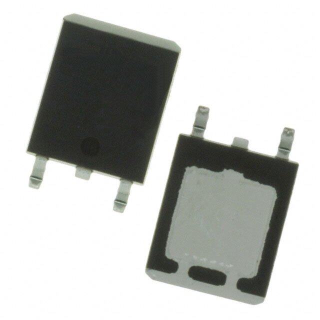
| 供应商器件封装 | D2PAK |
| 其它名称 | IRL1404STRLPBF-ND |
| 功率-最大值 | 3.8W |
| 包装 | 带卷 (TR) |
| 商标 | International Rectifier |
| 安装类型 | 表面贴装 |
| 安装风格 | SMD/SMT |
| 封装 | Reel |
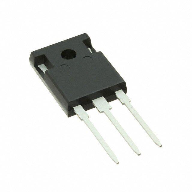
| 封装/外壳 | TO-263-3,D²Pak(2 引线+接片),TO-263AB |
| 封装/箱体 | D2PAK-2 |
| 工厂包装数量 | 800 |
| 晶体管极性 | N-Channel |
| 最大工作温度 | + 175 C |
| 标准包装 | 800 |
| 正向跨导-最小值 | 93 S |
| 漏源极电压(Vdss) | 40V |
| 电流-连续漏极(Id)(25°C时) | 160A (Tc) |
| 配置 | Single |


- 商务部:美国ITC正式对集成电路等产品启动337调查
- 曝三星4nm工艺存在良率问题 高通将骁龙8 Gen1或转产台积电
- 太阳诱电将投资9.5亿元在常州建新厂生产MLCC 预计2023年完工
- 英特尔发布欧洲新工厂建设计划 深化IDM 2.0 战略
- 台积电先进制程称霸业界 有大客户加持明年业绩稳了
- 达到5530亿美元!SIA预计今年全球半导体销售额将创下新高
- 英特尔拟将自动驾驶子公司Mobileye上市 估值或超500亿美元
- 三星加码芯片和SET,合并消费电子和移动部门,撤换高东真等 CEO
- 三星电子宣布重大人事变动 还合并消费电子和移动部门
- 海关总署:前11个月进口集成电路产品价值2.52万亿元 增长14.8%


PDF Datasheet 数据手册内容提取
PD - 95148 IRL1404SPbF IRL1404LPbF (cid:6) Advanced Process Technology HEXFET® Power MOSFET (cid:6) Ultra Low On-Resistance (cid:6) Dynamic dv/dt Rating D (cid:6) 175°C Operating Temperature VDSS = 40V (cid:6) Fast Switching (cid:6) Fully Avalanche Rated R = 0.004Ω DS(on) (cid:6) Lead-Free G Description I = 160A(cid:1) D Seventh Generation HEXFET® power MOSFETs from S International Rectifier utilize advanced processing techniques to achieve extremely low on-resistance per silicon area. This benefit, combined with the fast switching speed and ruggedized device design that HEXFET power MOSFETs are well known for, provides the designer with an extremely efficient and reliable device for use in a wide variety of applications. The D2Pak is a surface mount power package capable of accommodating die sizes up to HEX-4. It provides the highest power capability and the lowest possible on- resistance in any existing surface mount package. The D2Pak TO-262 D2Pak is suitable for high current applications because of IRL1404S IRL1404L its low internal connection resistance and can dissipate up to 2.0W in a typical surface mount application. The through-hole version (IRL1404L) is available for low- Absolute Maximum Ratings Parameter Max. Units I @ T = 25°C Continuous Drain Current, V @ 10V 160(cid:1) D C GS I @ T = 100°C Continuous Drain Current, V @ 10V 110(cid:1) A D C GS I Pulsed Drain Current (cid:2) 640 DM P @T = 25°C Power Dissipation 3.8 W D A P @T = 25°C Power Dissipation 200 W D C Linear Derating Factor 1.3 W/°C V Gate-to-Source Voltage ± 20 V GS E Single Pulse Avalanche Energy(cid:3) 520 mJ AS I Avalanche Current(cid:2) 95 A AR E Repetitive Avalanche Energy(cid:2) 20 mJ AR dv/dt Peak Diode Recovery dv/dt (cid:4) 5.0 V/ns T Operating Junction and -55 to + 175 J TSTG Storage Temperature Range °C Soldering Temperature, for 10 seconds 300 (1.6mm from case) Thermal Resistance Parameter Typ. Max. Units RθJC Junction-to-Case ––– 0.75 RθCS Case-to-Sink, Flat, Greased Surface 0.50 ––– °C/W RθJA Junction-to-Ambient (PCB Mounted)(cid:5) ––– 40 www.irf.com 1 04/19/04
IRL1404S/LPbF Electrical Characteristics @ T = 25°C (unless otherwise specified) J Parameter Min. Typ. Max. Units Conditions V(BR)DSS Drain-to-Source Breakdown Voltage 40 ––– ––– V VGS = 0V, ID = 250µA ∆V(BR)DSS/∆TJ Breakdown Voltage Temp. Coefficient ––– 0.038 ––– V/°C Reference to 25°C, D = 1mA RDS(on) Static Drain-to-Source On-Resistance ––– ––– 0.004 Ω VGS = 10V, ID = 95A (cid:7) 0.0059 VGS = 4.3V, ID = 40A (cid:7) VGS(th) Gate Threshold Voltage 1.0 ––– 3.0 V VDS = VGS, ID = 250µA gfs Forward Transconductance 93 ––– ––– S VDS = 25V, ID = 95A IDSS Drain-to-Source Leakage Current ––– ––– 20 µA VDS = 40V, VGS = 0V ––– ––– 250 VDS = 32V, VGS = 0V, TJ = 150°C IGSS GGaattee--ttoo--SSoouurrccee FRoervwearsrde LLeeaakkaaggee –––––– –––––– -220000 nA VVGGSS == -2200VV Qg Total Gate Charge ––– ––– 140 ID = 95A Qgs Gate-to-Source Charge ––– ––– 48 nC VDS = 32V Qgd Gate-to-Drain ("Miller") Charge ––– ––– 60 VGS = 5.0V, See Fig. 6 (cid:7) td(on) Turn-On Delay Time ––– 18 ––– ns VDD = 20V tr Rise Time ––– 270 ––– ID = 95A td(off) Turn-Off Delay Time ––– 38 ––– RG = 2.5Ω VGS = 4.5V tf Fall Time ––– 130 ––– RD = 0.25Ω (cid:7) LD Internal Drain Inductance ––– 4.5 ––– nH Between lead, D 6mm (0.25in.) L Internal Source Inductance ––– 7.5 ––– from package G S and center of die contact S Ciss Input Capacitance ––– 6600 ––– VGS = 0V Coss Output Capacitance ––– 1700 ––– pF VDS = 25V Crss Reverse Transfer Capacitance ––– 350 ––– ƒ = 1.0MHz, See Fig. 5 Coss Output Capacitance ––– 6700 ––– VGS = 0V, VDS = 1.0V, ƒ = 1.0MHz Coss Output Capacitance ––– 1500 ––– VGS = 0V, VDS = 32V, ƒ = 1.0MHz Coss eff. Effective Output Capacitance (cid:8) ––– 1500 ––– VGS = 0V, VDS = 0V to 32V Source-Drain Ratings and Characteristics Parameter Min. Typ. Max. Units Conditions IS Continuous Source Current ––– ––– 160(cid:1) MOSFET symbol D (Body Diode) showing the A ISM Pulsed Source Current integral reverse G ––– ––– 640 (Body Diode) (cid:2) p-n junction diode. S VSD Diode Forward Voltage ––– ––– 1.3 V TJ = 25°C, IS = 95A, VGS = 0V(cid:9)(cid:7) trr Reverse Recovery Time ––– 63 94 ns TJ = 25°C, IF = 95A Qrr Reverse RecoveryCharge ––– 170 250 nC di/dt = 100A/µs(cid:9)(cid:7) ton Forward Turn-On Time Intrinsic turn-on time is negligible (turn-on is dominated by LS+LD) 2 www.irf.com
IRL1404S/LPbF (cid:1) (cid:1) 1000 1000 VGS VGS TOP 15V TOP 15V 10V 10V A) 87..00VV A) 87..00VV ent ( 655...050VVV ent ( 655...050VVV urr BOTTOM4.3V 4.3V urr BOTTOM4.3V 4.3V C C e e c c our 100 our 100 S S o- o- n-t n-t ai ai Dr Dr I , D I , D (cid:1) (cid:1) 20µs PULSE WIDTH 20µs PULSE WIDTH TJ = 25°C T J = 175°C 10 10 0.1 1 10 100 0.1 1 10 100 VD S , Drain-to-Source Voltage (V) V D S , Drain-to-Source Voltage (V) Fig 1. Typical Output Characteristics Fig 2. Typical Output Characteristics 1000 2.5 (cid:1) ID=160A e c n A) a nt ( (cid:1)TJ = 25 ° C sist 2.0 e e urr (cid:1) n R I , Drain-to-Source CD 100 T(cid:1)J V2=0 D µ 1 Ss 7 =5P °U1 C5LVSE WIDTH R , Drain-to-Source ODS(on)(Normalized) 0011....0505 (cid:1)VGS=10V 4.0 5.0 6.0 7.0 8.0 -60 -40 -20 0 20 40 60 80 100120140160180 VG S , Gate-to-Source Voltage (V) T J , Junction Temperature( ° C) Fig 3. Typical Transfer Characteristics Fig 4. Normalized On-Resistance Vs. Temperature www.irf.com 3
IRL1404S/LPbF (cid:1) 10000 20 (cid:1) VGS=0V, f = 1MHz ID=95A C =C + C C SHORTED (cid:1) 8000 CCirossssss==CCggddss + Cggdd , ds e (V) 16 VVDDSS== 2302VV (cid:1) g pF) Ciss olta ce ( 6000 e V 12 n c cita our a S C, Cap 4000 ate-to- 8 G 2000 C(cid:1)oss V , GS 4 (cid:1) (cid:1) FOR TEST CIRCUIT Crss SEE FIGURE 1 3 0 0 1 10 100 0 100 200 300 400 500 V , Drain-to-Source Voltage (V) Q , Total Gate Charge (nC) DS G Fig 5. Typical Capacitance Vs. Fig 6. Typical Gate Charge Vs. Drain-to-Source Voltage Gate-to-Source Voltage 1000 10000 (cid:1) OPERATION IN THIS AREA LIMITED BY R DS(on) A) nt ( ain Curre 100 (cid:1)TJ = 175 ° C urrent (A)urrent (A) 1000 (cid:1)10us Dr CC se ain ain (cid:1)100us er DrDr I , RevSD 10 (cid:1)TJ = 25 ° C I , I , D 100 (cid:1) T = 25 ° C (cid:1)1ms C (cid:1) TJ= 175 ° C (cid:1)10ms V G S = 0 V Single Pulse 1 10 0.0 0.5 1.0 1.5 2.0 2.5 3.0 1 10 100 VS D ,Source-to-Drain Voltage (V) VD S , Drain-to-Source Voltage (V) Fig 7. Typical Source-Drain Diode Fig 8. Maximum Safe Operating Area Forward Voltage 4 www.irf.com
IRL1404S/LPbF 160 R D (cid:1)LIMITED BY PACKAGE VDS V GS D.U.T. 120 R nt (A) G +-VDD e urr 10V ain C 80 PDuultsye F Wacidtotrh ≤≤ 01. 1µ %s Dr I , D 40 VDS 90% 0 25 50 75 100 125 150 175 T , Case Temperature ( ° C) C 10% Fig 9. Maximum Drain Current Vs. VGS Case Temperature td(on) tr td(off) tf 1 D = 0.50 ) Z thJC 0.20 ( 0.1 0.10 e ns 0.05 o (cid:1) p s 0.02 e mal R0.01 0.01 (cid:1)(THESRINMGALLE R PEUSLPSOENSE) PDM t1 r e Th (cid:1)t2 Notes: 1. Duty factor D = t 1 / t2 2. Peak TJ=PDMx ZthJC + TC 0.001 0.00001 0.0001 0.001 0.01 0.1 1 t , Rectangular Pulse Duration (sec) 1 Fig 11. Maximum Effective Transient Thermal Impedance, Junction-to-Case www.irf.com 5
IRL1404S/LPbF (cid:1) )1200 15V mJ ID y ( TOP 39A rg1000 67A VDS L DRIVER Ene BOTTOM 95A e h 800 c RG D.U.T + n IAS - VDDA vala 600 20V A tp 0.01Ω e s ul Fig 12a. Unclamped Inductive Test Circuit P 400 e V(BR)DSS gl n tp Si 200 E , AS 0 25 50 75 100 125 150 175 Starting T , Junction Temperature( ° C) J IAS Fig 12c. Maximum Avalanche Energy Fig 12b. Unclamped Inductive Waveforms Vs. Drain Current CurrentRegulator SameTypeasD.U.T. Q G 10 V 50KΩ QGS QGD 12V .2µF .3µF + D.U.T. -VDS V G VGS 3mA Charge IG ID CurrentSamplingResistors Fig 13a. Basic Gate Charge Waveform Fig 13b. Gate Charge Test Circuit 6 www.irf.com
IRL1404S/LPbF Peak Diode Recovery dv/dt Test Circuit + Circuit Layout Considerations D.U.T* • Low Stray Inductance (cid:4) • Ground Plane • Low Leakage Inductance Current Transformer - + (cid:3) (cid:7) - + - (cid:2) RG • dv/dt controlled by RG + • ISD controlled by Duty Factor "D" - VDD • D.U.T. - Device Under Test V GS * Reverse Polarity of D.U.T for P-Channel Driver Gate Drive P.W. Period D = P.W. Period [V = 1 0 V ] *** GS D.U.T. I Waveform SD Reverse Recovery Body Diode Forward Current Current di/dt D.U.T. V Waveform DS Diode Recovery dv/dt [ V ] DD Re-Applied Voltage Body Diode Forward Drop Inductor Curent [ I ] Ripple ≤ 5% SD *** V = 5.0V for Logic Level and 3V Drive Devices GS Fig 14. For N-channel HEXFET® power MOSFETs www.irf.com 7
IRL1404S/LPbF D2Pak Package Outline Dimensions are shown in millimeters (inches) D2Pak Part Marking Information (Lead-Free) THIS IS AN IRF530S WITH PART NUMBER LOT CODE 8024 INTERNATIONAL ASSEMBLED ON WW 02, 2000 RECTIFIER F530S IN THE ASSEMBLY LINE "L" LOGO DATE CODE pNoosteit:io "nP "i nind iacsasteesm "bLleya ldin-eFree" ASSEMBLY YEAR 0 = 2000 LOT CODE WEEK 02 LINE L OR PART NUMBER INTERNATIONAL RECTIFIER F530S LOGO DATE CODE P = DESIGNATES LEAD-FREE ASSEMBLY PRODUCT (OPTIONAL) LOT CODE YEAR 0 = 2000 WEEK 02 A = ASSEMBLY SITE CODE 8 www.irf.com
IRL1404S/LPbF TO-262 Package Outline TO-262 Part Marking Information EXAMPLE: THIS IS AN IRL3103L LOT CODE 1789 PART NUMBER INTERNATIONAL ASSEMBLED ON WW 19, 1997 RECTIFIER IN THE ASSEMBLY LINE "C" LOGO Note: "P" in assembly line DATE CODE position indicates "Lead-Free" ASSEMBLY YEAR 7 = 1997 LOT CODE WEEK 19 LINE C OR PART NUMBER INTERNATIONAL RECTIFIER LOGO DATE CODE P = DESIGNATES LEAD-FREE ASSEMBLY PRODUCT (OPTIONAL) LOT CODE YEAR 7 = 1997 WEEK 19 A = ASSEMBLY SITE CODE www.irf.com 9
IRL1404S/LPbF D2Pak Tape & Reel Information Dimensions are shown in millimeters (inches) TRR 1.60 (.063) 1.50 (.059) 43..1900 ((..116513)) 11..6500 ((..006539)) 0.368 (.0145) 0.342 (.0135) FEED DIRECTION 1.85 (.073) 11.60 (.457) 1.65 (.065) 11.40 (.449) 1155..4222 ((..660091)) 2243..3900 ((..995471)) TRL 1.75 (.069) 10.90 (.429) 1.25 (.049) 10.70 (.421) 4.72 (.136) 16.10 (.634) 4.52 (.178) 15.90 (.626) FEED DIRECTION 13.50 (.532) 27.40 (1.079) 12.80 (.504) 23.90 (.941) 4 330.00 60.00 (2.362) (14.173) MIN. MAX. 30.40 (1.197) NOTES : MAX. 1. COMFORMS TO EIA-418. 26.40 (1.039) 4 2. CONTROLLING DIMENSION: MILLIMETER. 24.40 (.961) 34.. DINIMCLEUNDSEIOSN F MLAENAGSEU RDEISDT @OR HTUIOBN. @ OUTER EDGE. 3 Notes: (cid:2) Repetitive rating; pulse width limited by (cid:1)(cid:9)Calculated continuous current based on maximum allowable max. junction temperature. ( See fig. 11 ) junction temperature; for recommended current-handing of the (cid:3) Starting T = 25°C, L = 0.35mH package refer to Design Tip # 93-4. J RG = 25Ω, IAS = 95A. (See Figure 12) (cid:5)(cid:9)This is applied to D2Pak, When mounted on 1" square PCB (cid:4) ISD ≤ 95A, di/dt ≤ 160A/µs, VDD ≤ V(BR)DSS, (sFoRld-e4r ionrg G te-1c0h nMiqauteesri arel)f e. rF toor arepcpolimcamtioenn dneodte f o#oAtpNr-in9t9 a4n.d TJ ≤ 175°C (cid:7) Pulse width ≤ 300µs; duty cycle ≤ 2%. (cid:8) Coss eff. is a fixed capacitance that gives the same charging time as Coss while VDS is rising from 0 to 80% VDSS. Data and specifications subject to change without notice. This product has been designed and qualified for the Industrial market. Qualification Standards can be found on IR’s Web site. IR WORLD HEADQUARTERS: 233 Kansas St., El Segundo, California 90245, USA Tel: (310) 252-7105 TAC Fax: (310) 252-7903 Visit us at www.irf.com for sales contact information.04/04 10 www.irf.com
Note: For the most current drawings please refer to the IR website at: http://www.irf.com/package/