ICGOO在线商城 > 分立半导体产品 > 晶体管 - 双极 (BJT) - 射频 > BFM520,115

 Datasheet下载
- 型号: BFM520,115
- 制造商: NXP Semiconductors
- 库位|库存: xxxx|xxxx
- 要求:
| 数量阶梯 | 香港交货 | 国内含税 |
| +xxxx | $xxxx | ¥xxxx |
查看当月历史价格
查看今年历史价格
BFM520,115产品简介:
ICGOO电子元器件商城为您提供BFM520,115由NXP Semiconductors设计生产,在icgoo商城现货销售,并且可以通过原厂、代理商等渠道进行代购。 BFM520,115价格参考¥2.87-¥2.87。NXP SemiconductorsBFM520,115封装/规格:晶体管 - 双极 (BJT) - 射频, RF Transistor 2 NPN (Dual) 8V 70mA 9GHz 1W Surface Mount 6-TSSOP。您可以下载BFM520,115参考资料、Datasheet数据手册功能说明书,资料中有BFM520,115 详细功能的应用电路图电压和使用方法及教程。
NXP USA Inc. 的 BFM520,115 是一款高性能射频双极结型晶体管(RF BJT),适用于高频、低噪声的无线通信应用。该器件主要应用于工作频率在数百MHz至数GHz范围内的射频放大电路,特别适合用于蜂窝通信基础设施中的低噪声放大器(LNA)、中等功率驱动放大器以及射频接收模块。

BFM520,115 具有优异的噪声系数和高增益特性,使其在信号微弱或对信噪比要求较高的场景中表现出色,常见于GSM、CDMA、WCDMA、LTE等移动通信基站的前端模块。此外,该晶体管也广泛用于工业、科学和医疗(ISM)频段设备、无线接入点、远程无线传感器以及点对点微波通信系统中。

其高可靠性和稳定性还使其适用于户外通信设备和恶劣环境下的射频单元。由于采用成熟可靠的工艺制造,BFM520,115 在长时间运行中保持性能一致,适合对系统稳定性要求较高的应用场景。总体而言,这款晶体管是现代射频设计中实现高效、低噪声信号放大的理想选择,尤其适用于需要高灵敏度接收和稳定传输性能的通信系统。
| 参数 | 数值 |
| 产品目录 | |
| 描述 | TRANS NPN DUAL 70MA 8V 6TSSOP射频双极晶体管 NPN DL 70MA 8V 9GHZ |
| 产品分类 | RF 晶体管 (BJT)分离式半导体 |
| 品牌 | NXP Semiconductors |
| 产品手册 | |
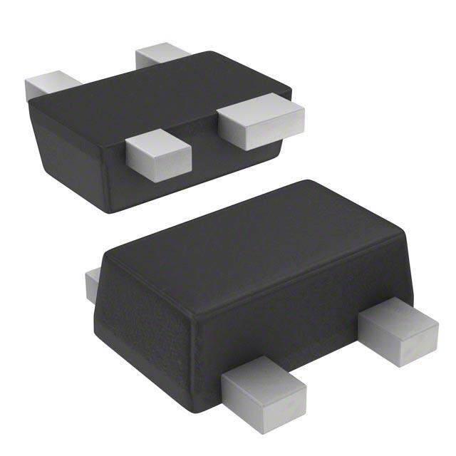
| 产品图片 |
|
| rohs | 符合RoHS无铅 / 符合限制有害物质指令(RoHS)规范要求 |
| 产品系列 | 晶体管,晶体管射频,射频双极晶体管,NXP Semiconductors BFM520,115- |
| 数据手册 | |
| 产品型号 | BFM520,115 |
| PCN封装 | |
| PCN设计/规格 | |
| 不同 Ic、Vce 时的DC电流增益(hFE)(最小值) | 60 @ 20mA,6V |
| 产品目录页面 | |
| 产品种类 | 射频双极晶体管 |
| 供应商器件封装 | 6-TSSOP |
| 其它名称 | 568-1646-2 |
| 功率-最大值 | 1W |
| 功率耗散 | 1000 mW |
| 包装 | 带卷 (TR) |
| 发射极-基极电压VEBO | 2.5 V |
| 商标 | NXP Semiconductors |
| 噪声系数(dB,不同f时的典型值) | 1.2dB ~ 2.1dB @ 900MHz |
| 增益 | - |
| 安装类型 | 表面贴装 |
| 安装风格 | SMD/SMT |
| 封装 | Reel |
| 封装/外壳 | 6-TSSOP,SC-88,SOT-363 |
| 封装/箱体 | SOT-363 |
| 工厂包装数量 | 3000 |
| 技术 | Silicon |
| 晶体管极性 | NPN |
| 晶体管类型 | 2 NPN(双) |
| 最大工作温度 | + 150 C |
| 最大工作频率 | 9000 MHz |
| 最大直流电集电极电流 | 0.07 A |
| 最小工作温度 | - 65 C |
| 标准包装 | 3,000 |
| 电压-集射极击穿(最大值) | 8V |
| 电流-集电极(Ic)(最大值) | 70mA |
| 类型 | RF Bipolar Small Signal |
| 配置 | Single |
| 集电极—发射极最大电压VCEO | 8 V |
| 集电极连续电流 | 0.07 A |
| 零件号别名 | BFM520 T/R |
| 频率 | 9000 MHz |
| 频率-跃迁 | 9GHz |


- 商务部:美国ITC正式对集成电路等产品启动337调查
- 曝三星4nm工艺存在良率问题 高通将骁龙8 Gen1或转产台积电
- 太阳诱电将投资9.5亿元在常州建新厂生产MLCC 预计2023年完工
- 英特尔发布欧洲新工厂建设计划 深化IDM 2.0 战略
- 台积电先进制程称霸业界 有大客户加持明年业绩稳了
- 达到5530亿美元!SIA预计今年全球半导体销售额将创下新高
- 英特尔拟将自动驾驶子公司Mobileye上市 估值或超500亿美元
- 三星加码芯片和SET,合并消费电子和移动部门,撤换高东真等 CEO
- 三星电子宣布重大人事变动 还合并消费电子和移动部门
- 海关总署:前11个月进口集成电路产品价值2.52万亿元 增长14.8%

PDF Datasheet 数据手册内容提取
DISCRETE SEMICONDUCTORS DATA SHEET BFM520 Dual NPN wideband transistor Product specification 1996 Oct 08 Supersedes data of 1995 Sep 04
NXP Semiconductors Product specification Dual NPN wideband transistor BFM520 FEATURES PINNING - SOT363A Small size PIN SYMBOL DESCRIPTION Temperature and h matched FE 1 b base1 1 Low noise and high gain 2 e emitter1 1 High gain at low current and low capacitance at low 3 c collector2 2 voltage 4 b base2 2 Gold metallization ensures excellent reliability. 5 e emitter2 2 6 c collector1 1 APPLICATIONS Oscillator and buffer amplifiers 6 5 4 Balanced amplifiers handbook, halfpage c1 c2 LNA/mixers. b1 b2 DESCRIPTION e1 e2 Dual transistor with two silicon NPN RF dies in a surface 1 2 3 mount 6-pin SOT363 (S-mini) package. Thetransistor is Top view MAM210 primarily intended for wideband applications in the GHz-range in the RF front end of analog and digital cellular Marking code: N2. phones, cordless phones, radar detectors, pagers and Fig.1 Simplified outline and symbol. satellite TV-tuners. QUICK REFERENCE DATA SYMBOL PARAMETER CONDITIONS MIN. TYP. MAX. UNIT Any single transistor C feedback capacitance I =0; V =3V; f=1MHz 0.4 pF re e CB f transition frequency I =20mA; V =3V; f=900MHz 9 GHz T C CE s 2 insertion power gain IC=20mA; VCE=3V; 13 14.5 dB 21 f=900MHz; T =25C amb G maximum unilateral power gain I =20mA; V =3V; 15 dB UM C CE f=900MHz; T =25C amb F noise figure I =5mA; V =3V; 1.2 1.6 dB C CE f=900MHz; = S opt R thermal resistance from junction single loaded 230 K/W thj-s to soldering point double loaded 115 K/W 1996Oct08 2
NXP Semiconductors Product specification Dual NPN wideband transistor BFM520 LIMITING VALUES In accordance with the Absolute Maximum System (IEC134). SYMBOL PARAMETER CONDITIONS MIN. MAX. UNIT Any single transistor V collector-base voltage open emitter 20 V CBO V collector-emitter voltage open base 8 V CEO V emitter-base voltage open collector 2.5 V EBO I DC collector current 70 mA C P total power dissipation up to T =118C; note1 1 W tot s T storage temperature 65 +175 C stg T junction temperature 175 C j THERMAL CHARACTERISTICS SYMBOL PARAMETER CONDITIONS VALUE UNIT R thermal resistance from junction single loaded 230 K/W thj-s to soldering point; note1 double loaded 115 K/W Note to the Limiting values and Thermal characteristics 1. T is the temperature at the soldering point of the collector pin. s 1996Oct08 3
NXP Semiconductors Product specification Dual NPN wideband transistor BFM520 CHARACTERISTICS T =25C unless otherwise specified. j SYMBOL PARAMETER CONDITIONS MIN. TYP. MAX. UNIT DC characteristics of any single transistor V collector-base breakdown voltage I =2.5A; I =0 20 V (BR)CBO C E V collector-emitter breakdown voltage I =10A; I =0 8 V (BR)CEO C B V emitter-base breakdown voltage I =2.5A; I =0 2.5 V (BR)EBO E C I collector-base leakage current V =6V; I =0 50 nA CBO CB E h DC current gain I =20mA; V =6V 60 120 250 FE C CE DC characteristics of the dual transistor h ratio of highest and lowest DC I =I =20mA; 1 1.2 FE C1 C2 current gain V =V =6V CE1 CE2 V difference between highest and I =I =30mA; T =25C 0 1 mV BEO E1 E2 amb lowest base-emitter voltage (offset voltage) AC characteristics of any single transistor f transition frequency I =20mA; V =3V; f=1GHz 9 GHz T C CE C collector capacitance I =i =0; V =3V; f=1MHz 0.5 pF c E e CB C feedback capacitance I =0; V =3V; f=1MHz 0.4 pF re C CB G maximum unilateral power gain; I =20mA; V =3V; 15 dB UM C CE note1 T =25C; f=900MHz amb I =20mA; V =3V; 9 dB C CE T =25C; f=2GHz amb s 2 insertion power gain IC=20mA; VCE=3V; 13 14.5 dB 21 f=900MHz; T =25C amb F noise figure I =5mA; V =3V; 1.2 1.6 dB C CE f=900MHz; = S opt I =20mA; V =3V; 1.7 2.1 dB C CE f=900MHz; = S opt I =5mA; V =3V; 1.9 dB C CE f=2GHz; = S opt Note s 2 1. G is the maximum unilateral power gain, assuming s is zero. G = 10 log---------------------------2--1--------------------------- dB UM 12 UM 1– s 21– s 2 11 22 1996Oct08 4
NXP Semiconductors Product specification Dual NPN wideband transistor BFM520 MBG228 MRA705 1.5 12 handbook, halfpage handbook, halfpage Ptot fT (mW) (GHz) VCE = 6V double loaded 1 8 VCE = 3V single loaded 0.5 4 0 0 50 100 150 Ts (oC)200 010−1 1 10 IC (mA) 102 f=1GHz; Tamb=25C. Fig.2 Power derating as a function of soldering Fig.3 Transition frequency as a function of point temperature; typical values. collector current; typical values. MRA703 MRA704 250 0.6 handbook, halfpage handbook, halfpage hFE Cre (pF) 200 0.4 150 100 0.2 50 010−2 10−1 1 10 IC (mA)102 00 4 8 VCB (V) 12 VCE=6V. IC=0; f=1MHz. Fig.4 DC current gain as a function of collector Fig.5 Feedback capacitance as a function of current; typical values. collector-base voltage; typical values. 1996Oct08 5
NXP Semiconductors Product specification Dual NPN wideband transistor BFM520 MGG203 MGG204 20 20 handbook, halfpage handbook, halfpage gain gain (dB) MSG/Gmax (dB) 16 16 GUM 12 12 MSG/Gmax 8 8 GUM 4 4 0 0 0 10 20 30 0 10 20 30 IC (mA) IC (mA) f=900MHz; VCE=3V. f=2GHz; VCE=3V. Fig.6 Gain as a function of collector current; Fig.7 Gain as a function of collector current; typical values. typical values. MGG205 MGG206 50 50 handbook, halfpage handbook, halfpage gain gain (dB) (dB) 40 40 GUM GUM MSG/Gmax 30 30 MSG/Gmax 20 20 10 10 0 0 10 102 103 104 10 102 103 104 f (MHz) f (MHz) IC=5mA; VCE=3V. IC=20 mA; VCE=3V. Fig.8 Gain as a function of frequency; typical Fig.9 Gain as a function of frequency; typical values. values. 1996Oct08 6
NXP Semiconductors Product specification Dual NPN wideband transistor BFM520 MRA714 MRA715 5 20 5 20 handbook, halfpage handbook, halfpage Fmin Gass Fmin IC = 5 mA 20 mA Gass (dB) f = 900 MHz (dB) (dB) Gass (dB) 4 15 4 15 1000 MHz Gass 3 10 3 10 2000 MHz 2 5 2 5 2000 MHz 1000 MHz Fmin 20 mA Fmin 1 0 1 0 900 MHz 5 mA 500 MHz 0 −5 0 −5 1 10 102 102 103 104 IC (mA) f (MHz) VCE=3V. VCE=3V. Fig.10 Minimum noise figure and associated Fig.11 Minimum noise figure and associated available gain as functions of collector available gain as functions of frequency. current. 1996Oct08 7
NXP Semiconductors Product specification Dual NPN wideband transistor BFM520 APPLICATION INFORMATION SPICE parameters for any single BFM520 die C1 C2 handbook, halfpage SEQUENCE No. PARAMETER VALUE UNIT 1 IS 1.016 fA LP LP 2 BF 220.1 3 NF 1.000 B1 T1 T2 B2 4 VAF 48.06 V LB LB 5 IKF 510.0 mA LE LE 6 ISE 283.0 fA 7 NE 2.035 E1 E2 MBG188 8 BR 100.7 9 NR 0.988 10 VAR 1.692 V Fig.12 Package equivalent circuit SOT363A 11 IKR 2.352 mA (inductance only). 12 ISC 24.48 aA 13 NC 1.022 14 RB 10.00 15 IRB 1.000 A 16 RBM 10.00 Lead inductances (nH) 17 RE 0.775 18 RC 2.210 LP 0.4 19(1) XTB 0.000 LB 0.6 20(1) EG 1.110 eV 21(1) XTI 3.000 LE 1.0 22 CJE 1.245 pF 23 VJE 600.0 mV 24 MJE 0.258 25 TF 8.616 ps E2 3 26 XTF 6.788 27 VTF 1.414 V E1 27 6 28 ITF 110.3 mA B2 1 27 3 29 PTF 45.01 deg 30 CJC 447.6 fF C2 3 17 36 48 31 VJC 189.2 mV 32 MJC 0.071 C1 48 36 17 3 6 33 XCJC 0.130 MBG189 34 TR 543.7 ps B1 E2 E1 B2 C2 35(1) CJS 0.000 F 36(1) VJS 750.0 mV 37(1) MJS 0.000 Fig.13 Package capacitance (fF) between indicated nodes. 38 FC 0.780 Note 1. These parameters have not been extracted, thedefault values are shown. 1996Oct08 8
NXP Semiconductors Product specification Dual NPN wideband transistor BFM520 PACKAGE OUTLINE Plastic surface-mounted package; 6 leads SOT363 D B E A X y HE v M A 6 5 4 Q pin 1 index A A1 1 2 3 c e1 bp w M B Lp e detail X 0 1 2 mm scale DIMENSIONS (mm are the original dimensions) A1 UNIT A max bp c D E e e1 HE Lp Q v w y 1.1 0.30 0.25 2.2 1.35 2.2 0.45 0.25 mm 0.1 1.3 0.65 0.2 0.2 0.1 0.8 0.20 0.10 1.8 1.15 2.0 0.15 0.15 OUTLINE REFERENCES EUROPEAN ISSUE DATE VERSION IEC JEDEC JEITA PROJECTION 04-11-08 SOT363 SC-88 06-03-16 1996Oct08 9
NXP Semiconductors Product specification Dual NPN wideband transistor BFM520 DATA SHEET STATUS DOCUMENT PRODUCT DEFINITION STATUS(1) STATUS(2) Objective data sheet Development This document contains data from the objective specification for product development. Preliminary data sheet Qualification This document contains data from the preliminary specification. Product data sheet Production This document contains the product specification. Notes 1. Please consult the most recently issued document before initiating or completing a design. 2. The product status of device(s) described in this document may have changed since this document was published and may differ in case of multiple devices. The latest product status information is available on the Internet at URLhttp://www.nxp.com. DEFINITIONS Right to make changes NXP Semiconductors reserves the right to make changes to information Product specification The information and data published in this document, including without limitation provided in a Product data sheet shall define the specifications and product descriptions, at any time and specification of the product as agreed between NXP without notice. This document supersedes and replaces all Semiconductors and its customer, unless NXP information supplied prior to the publication hereof. Semiconductors and customer have explicitly agreed otherwise in writing. In no event however, shall an Suitability for use NXP Semiconductors products are agreement be valid in which the NXP Semiconductors not designed, authorized or warranted to be suitable for product is deemed to offer functions and qualities beyond use in life support, life-critical or safety-critical systems or those described in the Product data sheet. equipment, nor in applications where failure or malfunction of an NXP Semiconductors product can reasonably be expected to result in personal injury, death or severe DISCLAIMERS property or environmental damage. NXP Semiconductors Limited warranty and liability Information in this accepts no liability for inclusion and/or use of NXP document is believed to be accurate and reliable. Semiconductors products in such equipment or However, NXP Semiconductors does not give any applications and therefore such inclusion and/or use is at representations or warranties, expressed or implied, as to the customer’s own risk. the accuracy or completeness of such information and Applications Applications that are described herein for shall have no liability for the consequences of use of such any of these products are for illustrative purposes only. information. NXP Semiconductors makes no representation or In no event shall NXP Semiconductors be liable for any warranty that such applications will be suitable for the indirect, incidental, punitive, special or consequential specified use without further testing or modification. damages (including - without limitation - lost profits, lost Customers are responsible for the design and operation of savings, business interruption, costs related to the their applications and products using NXP removal or replacement of any products or rework Semiconductors products, and NXP Semiconductors charges) whether or not such damages are based on tort accepts no liability for any assistance with applications or (including negligence), warranty, breach of contract or any customer product design. It is customer’s sole other legal theory. responsibility to determine whether the NXP Notwithstanding any damages that customer might incur Semiconductors product is suitable and fit for the for any reason whatsoever, NXP Semiconductors’ customer’s applications and products planned, as well as aggregate and cumulative liability towards customer for for the planned application and use of customer’s third the products described herein shall be limited in party customer(s). Customers should provide appropriate accordance with the Terms and conditions of commercial design and operating safeguards to minimize the risks sale of NXP Semiconductors. associated with their applications and products. 1996Oct08 10
NXP Semiconductors Product specification Dual NPN wideband transistor BFM520 NXP Semiconductors does not accept any liability related Export control This document as well as the item(s) to any default, damage, costs or problem which is based described herein may be subject to export control on any weakness or default in the customer’s applications regulations. Export might require a prior authorization from or products, or the application or use by customer’s third national authorities. party customer(s). Customer is responsible for doing all Quick reference data The Quick reference data is an necessary testing for the customer’s applications and extract of the product data given in the Limiting values and products using NXP Semiconductors products in order to Characteristics sections of this document, and as such is avoid a default of the applications and the products or of not complete, exhaustive or legally binding. the application or use by customer’s third party customer(s). NXP does not accept any liability in this Non-automotive qualified products Unless this data respect. sheet expressly states that this specific NXP Semiconductors product is automotive qualified, the Limiting values Stress above one or more limiting product is not suitable for automotive use. It is neither values (as defined in the Absolute Maximum Ratings qualified nor tested in accordance with automotive testing System of IEC60134) will cause permanent damage to or application requirements. NXP Semiconductors accepts the device. Limiting values are stress ratings only and no liability for inclusion and/or use of non-automotive (proper) operation of the device at these or any other qualified products in automotive equipment or conditions above those given in the Recommended applications. operating conditions section (if present) or the Characteristics sections of this document is not warranted. In the event that customer uses the product for design-in Constant or repeated exposure to limiting values will and use in automotive applications to automotive permanently and irreversibly affect the quality and specifications and standards, customer (a) shall use the reliability of the device. product without NXP Semiconductors’ warranty of the product for such automotive applications, use and Terms and conditions of commercial sale NXP specifications, and (b) whenever customer uses the Semiconductors products are sold subject to the general product for automotive applications beyond NXP terms and conditions of commercial sale, as published at Semiconductors’ specifications such use shall be solely at http://www.nxp.com/profile/terms, unless otherwise customer’s own risk, and (c) customer fully indemnifies agreed in a valid written individual agreement. In case an NXP Semiconductors for any liability, damages or failed individual agreement is concluded only the terms and product claims resulting from customer design and use of conditions of the respective agreement shall apply. NXP the product for automotive applications beyond NXP Semiconductors hereby expressly objects to applying the Semiconductors’ standard warranty and NXP customer’s general terms and conditions with regard to the Semiconductors’ product specifications. purchase of NXP Semiconductors products by customer. No offer to sell or license Nothing in this document may be interpreted or construed as an offer to sell products that is open for acceptance or the grant, conveyance or implication of any license under any copyrights, patents or other industrial or intellectual property rights. 1996Oct08 11
NXP Semiconductors provides High Performance Mixed Signal and Standard Product solutions that leverage its leading RF, Analog, Power Management, Interface, Security and Digital Processing expertise Customer notification This data sheet was changed to reflect the new company name NXP Semiconductors, including new legal definitions and disclaimers. No changes were made to the technical content, except for package outline drawings which were updated to the latest version. Contact information For additional information please visit: http://www.nxp.com For sales offices addresses send e-mail to: salesaddresses@nxp.com © NXP B.V. 2010 All rights are reserved. Reproduction in whole or in part is prohibited without the prior written consent of the copyright owner. The information presented in this document does not form part of any quotation or contract, is believed to be accurate and reliable and may be changed without notice. No liability will be accepted by the publisher for any consequence of its use. Publication thereof does not convey nor imply any license under patent- or other industrial or intellectual property rights. Printed in The Netherlands R77/02/pp12 Date of release: 1996Oct08