ICGOO在线商城 > 分立半导体产品 > 晶体管 - 双极 (BJT) - 阵列 > BC856BDW1T1G
 Datasheet下载
- 型号: BC856BDW1T1G
- 制造商: ON Semiconductor
- 库位|库存: xxxx|xxxx
- 要求:
| 数量阶梯 | 香港交货 | 国内含税 |
| +xxxx | $xxxx | ¥xxxx |
查看当月历史价格
查看今年历史价格
BC856BDW1T1G产品简介:
ICGOO电子元器件商城为您提供BC856BDW1T1G由ON Semiconductor设计生产,在icgoo商城现货销售,并且可以通过原厂、代理商等渠道进行代购。 BC856BDW1T1G价格参考。ON SemiconductorBC856BDW1T1G封装/规格:晶体管 - 双极 (BJT) - 阵列, Bipolar (BJT) Transistor Array 2 PNP (Dual) 65V 100mA 100MHz 380mW Surface Mount SC-88/SC70-6/SOT-363。您可以下载BC856BDW1T1G参考资料、Datasheet数据手册功能说明书,资料中有BC856BDW1T1G 详细功能的应用电路图电压和使用方法及教程。
BC856BDW1T1G是安森美(ON Semiconductor)生产的一款双极结型晶体管(BJT)阵列器件,属于PNP型晶体管,采用SOT-26封装,内部集成了两个独立的PNP晶体管。该型号具有高可靠性、小型化和良好的开关与放大性能,广泛应用于各类电子电路中。

其典型应用场景包括:便携式电子设备中的信号切换与电平转换,如智能手机、平板电脑和可穿戴设备;在电源管理电路中用于负载开关或电压检测;在消费类电子产品如电视、机顶盒、音响设备中实现逻辑驱动和小信号放大;还可用于LED驱动电路中的电流控制与开关功能。

由于其低功耗特性和紧凑封装,BC856BDW1T1G非常适合空间受限的高密度PCB设计。此外,在工业控制、通信模块和传感器接口电路中也常被用作放大器或开关元件,实现信号调理与驱动功能。其一致的电气特性与高增益表现,确保了系统运行的稳定性与可靠性。

综上,BC856BDW1T1G主要适用于需要小型化、低功耗和稳定性能的模拟与数字混合电路场景,是现代电子设备中常用的通用型双晶体管阵列解决方案。
| 参数 | 数值 |
| 产品目录 | |
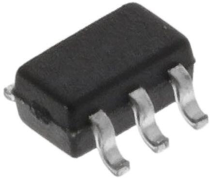
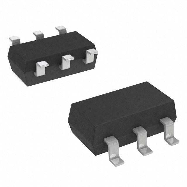
| 描述 | TRANS DUAL PNP 65V 100MA SOT363两极晶体管 - BJT 100mA 80V Dual PNP |
| 产品分类 | 晶体管(BJT) - 阵列分离式半导体 |
| 品牌 | ON Semiconductor |
| 产品手册 | |
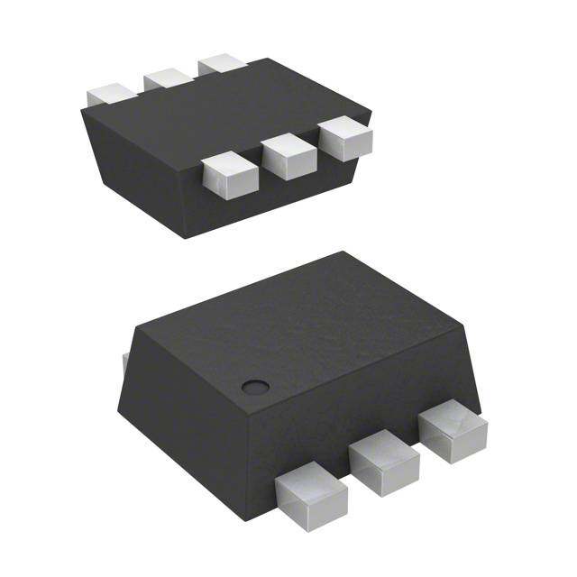
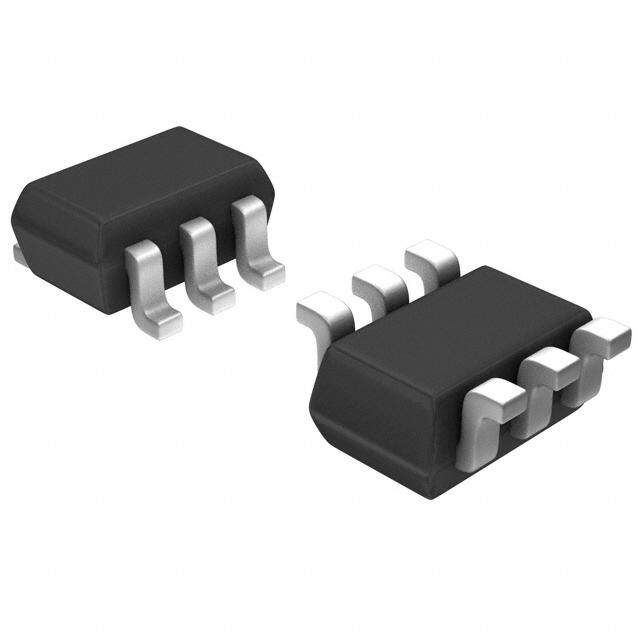
| 产品图片 |
|
| rohs | 符合RoHS无铅 / 符合限制有害物质指令(RoHS)规范要求 |
| 产品系列 | 晶体管,两极晶体管 - BJT,ON Semiconductor BC856BDW1T1G- |
| 数据手册 | |
| 产品型号 | BC856BDW1T1G |
| PCN设计/规格 | |
| 不同 Ib、Ic时的 Vce饱和值(最大值) | 650mV @ 5mA,100mA |
| 不同 Ic、Vce 时的DC电流增益(hFE)(最小值) | 220 @ 2mA,5V |
| 产品种类 | 两极晶体管 - BJT |
| 供应商器件封装 | SC-88/SC70-6/SOT-363 |
| 其它名称 | BC856BDW1T1GOSDKR |
| 功率-最大值 | 380mW |
| 包装 | Digi-Reel® |
| 发射极-基极电压VEBO | 5 V |
| 商标 | ON Semiconductor |
| 增益带宽产品fT | 100 MHz |
| 安装类型 | 表面贴装 |
| 安装风格 | SMD/SMT |
| 封装 | Reel |
| 封装/外壳 | 6-TSSOP,SC-88,SOT-363 |
| 封装/箱体 | SC-70-6 |
| 工厂包装数量 | 3000 |
| 晶体管极性 | PNP |
| 晶体管类型 | 2 PNP(双) |
| 最大功率耗散 | 380 mW |
| 最大工作温度 | + 150 C |
| 最大直流电集电极电流 | 0.1 A |
| 最小工作温度 | - 55 C |
| 标准包装 | 1 |
| 电压-集射极击穿(最大值) | 65V |
| 电流-集电极(Ic)(最大值) | 100mA |
| 电流-集电极截止(最大值) | - |
| 直流集电极/BaseGainhfeMin | 220 |
| 系列 | BC856B |
| 配置 | Dual |
| 集电极—发射极最大电压VCEO | - 65 V |
| 集电极—基极电压VCBO | - 80 V |
| 集电极—射极饱和电压 | - 0.65 V |
| 集电极连续电流 | - 0.1 A |
| 频率-跃迁 | 100MHz |


- 商务部:美国ITC正式对集成电路等产品启动337调查
- 曝三星4nm工艺存在良率问题 高通将骁龙8 Gen1或转产台积电
- 太阳诱电将投资9.5亿元在常州建新厂生产MLCC 预计2023年完工
- 英特尔发布欧洲新工厂建设计划 深化IDM 2.0 战略
- 台积电先进制程称霸业界 有大客户加持明年业绩稳了
- 达到5530亿美元!SIA预计今年全球半导体销售额将创下新高
- 英特尔拟将自动驾驶子公司Mobileye上市 估值或超500亿美元
- 三星加码芯片和SET,合并消费电子和移动部门,撤换高东真等 CEO
- 三星电子宣布重大人事变动 还合并消费电子和移动部门
- 海关总署:前11个月进口集成电路产品价值2.52万亿元 增长14.8%


PDF Datasheet 数据手册内容提取
BC856BDW1T1G, SBC856BDW1T1G(cid:2)Series, BC857BDW1T1G, SBC857BDW1T1G(cid:2)Series, BC858CDW1T1G Series Dual General Purpose www.onsemi.com Transistors PNP Duals SOT−363/SC−88 These transistors are designed for general purpose amplifier CASE 419B applications. They are housed in the SOT−363/SC−88 which is STYLE 1 designed for low power surface mount applications. (3) (2) (1) Features • S Prefix for Automotive and Other Applications Requiring Unique Site and Control Change Requirements; AEC−Q101 Qualified and Q1 Q2 PPAP Capable • These Devices are Pb−Free, Halogen Free/BFR Free and are RoHS Compliant* (4) (5) (6) MAXIMUM RATINGS MARKING DIAGRAM Rating Symbol Value Unit 6 Collector−Emitter Voltage VCEO V BC856, SBC856 −65 3x M(cid:2) BC857, SBC857 −45 (cid:2) BC858 −30 Collector−Base Voltage VCBO V 1 BC856, SBC856 −80 BC857, SBC857 −50 3x = Specific Device Code BC858 −30 x = B, F, G, or L Emitter−Base Voltage VEBO −5.0 V (See Ordering Information) M = Date Code Collector Current −Continuous IC −100 mAdc (cid:2) = Pb−Free Package Collector Current − Peak IC −200 mAdc (Note: Microdot may be in either location) THERMAL CHARACTERISTICS ORDERING INFORMATION Characteristic Symbol Max Unit See detailed ordering and shipping information in the package Total Device Dissipation PD 380 mW dimensions section on page 6 of this data sheet. Per Device 250 mW FR−5 Board (Note 1) TA = 25°C Derate Above 25°C 3.0 mW/°C Thermal Resistance, R(cid:2)JA °C/W Junction−to−Ambient 328 Junction and Storage Temperature TJ, Tstg −55 to +150 °C Range Stresses exceeding those listed in the Maximum Ratings table may damage the device. If any of these limits are exceeded, device functionality should not be assumed, damage may occur and reliability may be affected. 1. FR−5 = 1.0 x 0.75 x 0.062 in *For additional information on our Pb−Free strategy and soldering details, please download the ON Semiconductor Soldering and Mounting Techniques Reference Manual, SOLDERRM/D. © Semiconductor Components Industries, LLC, 2013 1 Publication Order Number: August, 2016 − Rev. 10 BC856BDW1T1/D
BC856BDW1T1G, SBC856BDW1T1G Series, BC857BDW1T1G, SBC857BDW1T1G Series, BC858CDW1T1G Series ELECTRICAL CHARACTERISTICS (TA = 25°C unless otherwise noted) Characteristic Symbol Min Typ Max Unit OFF CHARACTERISTICS Collector−Emitter Breakdown Voltage V(BR)CEO V (IC = −10 mA) BC856, SBC856 Series −65 − − BC857, SBC857 Series −45 − − BC858 Series −30 − − Collector−Emitter Breakdown Voltage V(BR)CES V (IC = −10 (cid:3)A, VEB = 0) BC856, SBC856 Series −80 − − BC857B, SBC857B Only −50 − − BC858 Series −30 − − Collector−Base Breakdown Voltage V(BR)CBO V (IC = −10 (cid:3)A) BC856, SBC856 Series −80 − − BC857, SBC857 Series −50 − − BC858 Series −30 − − Emitter−Base Breakdown Voltage V(BR)EBO V (IE = −1.0 (cid:3)A) BC856, SBC856 Series −5.0 − − BC857, SBC857 Series −5.0 − − BC858 Series −5.0 − − Collector Cutoff Current ICBO (VCB = −30 V) − − −15 nA (VCB = −30 V, TA = 150°C) − − −4.0 (cid:3)A ON CHARACTERISTICS DC Current Gain hFE − (IC = −10 (cid:3)A, VCE = −5.0 V) BC856B, SBC856B, BC857B, SBC857B − 150 − BC857C, SBC857C, BC858C − 270 − (IC = −2.0 mA, VCE = −5.0 V) BC856B, SBC856B, BC857B, SBC857B 220 290 475 BC857C, SBC857C, BC858C 420 520 800 Collector−Emitter Saturation Voltage VCE(sat) V (IC = −10 mA, IB = −0.5 mA) − − −0.3 (IC = −100 mA, IB = −5.0 mA) − − −0.65 Base−Emitter Saturation Voltage VBE(sat) V (IC = −10 mA, IB = −0.5 mA) − −0.7 − (IC = −100 mA, IB = −5.0 mA) − −0.9 − Base−Emitter On Voltage VBE(on) V (IC = −2.0 mA, VCE = −5.0 V) −0.6 − −0.75 (IC = −10 mA, VCE = −5.0 V) − − −0.82 SMALL−SIGNAL CHARACTERISTICS Current−Gain − Bandwidth Product fT MHz (IC = −10 mA, VCE = −5.0 Vdc, f = 100 MHz) 100 − − Output Capacitance Cob pF (VCB = −10 V, f = 1.0 MHz) − − 4.5 Noise Figure NF dB (IC = −0.2 mA, VCE = −5.0 Vdc, RS = 2.0 k(cid:4), f = 1.0 kHz, BW = 200 Hz) − − 10 www.onsemi.com 2
BC856BDW1T1G, SBC856BDW1T1G Series, BC857BDW1T1G, SBC857BDW1T1G Series, BC858CDW1T1G Series TYPICAL CHARACTERISTICS − BC856/SBC856 -1.0 ED) TJ = 25°C RMALIZ VTAC E= =2 5-°5C.0 V -0.8 VBE(sat) @ IC/IB = 10 O S) N 2.0 T N ( OL -0.6 GAI 1.0 E (V VBE @ VCE = -5.0 V T G N A CURRE 0.5 V, VOLT -0.4 DC -0.2 , FE 0.2 VCE(sat) @ IC/IB = 10 h 0 -0.1 -0.2 -1.0-2.0 -5.0 -10 -20 -50 -100-200 -0.2 -0.5 -1.0 -2.0 -5.0 -10 -20 -50 -100 -200 IC, COLLECTOR CURRENT (mA) IC, COLLECTOR CURRENT (mA) Figure 1. DC Current Gain Figure 2. “On” Voltage S) -2.0 -1.0 LT C) O ° R-EMITTER VOLTAGE (V ---110...268 -1I0C m=A -20 mA -50 mA -100 mA -200 mA URE COEFFICIENT (mV/ ---112...482 (cid:2)VB for VBE -55°C to 125°C O AT LLECT -0.4 MPER -2.6 O E V, CCE 0 TJ = 25°C θ, TVB -3.0 -0.02 -0.05 -0.1 -0.2 -0.5 -1.0 -2.0 -5.0 -10 -20 -0.2 -0.5 -1.0 -2.0 -5.0 -10 -20 -50 -100 -200 IB, BASE CURRENT (mA) IC, COLLECTOR CURRENT (mA) Figure 3. Collector Saturation Region Figure 4. Base−Emitter Temperature Coefficient 40 T C DU VCE = -5.0 V TJ = 25°C RO 500 P F) 20 Cib TH p D E ( WI 200 C D N N PACITA 81.00 N - BA 100 A AI C 6.0 G 50 C, Cob T- N E 4.0 R R 20 U C (cid:2), T 2.0 f -0.1 -0.2 -0.5 -1.0 -2.0 -5.0 -10 -20 -50 -100 -1.0 -10 -100 VR, REVERSE VOLTAGE (VOLTS) IC, COLLECTOR CURRENT (mA) Figure 5. Capacitance Figure 6. Current−Gain − Bandwidth Product www.onsemi.com 3
BC856BDW1T1G, SBC856BDW1T1G Series, BC857BDW1T1G, SBC857BDW1T1G Series, BC858CDW1T1G Series TYPICAL CHARACTERISTICS − BC857/SBC857/BC858 2.0 -1.0 AIN 1.5 VCE = -10 V -0.9 TA = 25°C T G TA = 25°C -0.8 VBE(sat) @ IC/IB = 10 N RE 1.0 S) -0.7 ED DC CUR 0.7 TAGE (VOLT --00..65 VBE(on) @ VCE = -10 V LIZ 0.5 OL -0.4 A V M V, -0.3 R O N -0.2 h, FE 0.3 -0.1 VCE(sat) @ IC/IB = 10 0.2 0 -0.2 -0.5 -1.0 -2.0 -5.0 -10 -20 -50 -100 -200 -0.1 -0.2 -0.5 -1.0 -2.0 -5.0 -10 -20 -50 -100 IC, COLLECTOR CURRENT (mAdc) IC, COLLECTOR CURRENT (mAdc) Figure 7. Normalized DC Current Gain Figure 8. “Saturation” and “On” Voltages -2.0 1.0 LTAGE (V) -1.6 TA = 25°C °T (mV/C) 1.2 -55°C to +125°C O N V E R CI 1.6 TE -1.2 FFI T E EMI CO 2.0 CTOR- -0.8 -IC1 0= mA IC = -50 mA IC = -200 mA ATURE 2.4 V, COLLECE -0.4 IC = -20 mA IC = -100 mA , TEMPERVB 2.8 0 θ -0.02 -0.1 -1.0 -10 -20 -0.2 -1.0 -10 -100 IB, BASE CURRENT (mA) IC, COLLECTOR CURRENT (mA) Figure 9. Collector Saturation Region Figure 10. Base−Emitter Temperature Coefficient z) 10 H 400 M Cib T ( 300 C 7.0 U TA = 25°C OD 200 R TANCE (pF) 53..00 Cob NDWIDTH P 110500 VTAC E= =2 5-°1C0 V CI A 80 A B CAP N - 60 C, 2.0 GAI - 40 T N E 30 R R U C 1.0-0.4 -0.6 -1.0 -2.0 -4.0 -6.0 -10 -20 -30 -40 f(cid:2), T 20-0.5 -1.0 -2.0 -3.0 -5.0 -10 -20 -30 -50 VR, REVERSE VOLTAGE (VOLTS) IC, COLLECTOR CURRENT (mAdc) Figure 11. Capacitances Figure 12. Current−Gain − Bandwidth Product www.onsemi.com 4
BC856BDW1T1G, SBC856BDW1T1G Series, BC857BDW1T1G, SBC857BDW1T1G Series, BC858CDW1T1G Series 1.0 D = 0.5 HERMALMALIZED) 0.1 000.0..125 TR SIENT CE (NO 0.02 P(pk) ZR(cid:2)(cid:2)JJAA( t=) =3 2r8(t°)C R/W(cid:2)JA MAX NN D CURVES APPLY FOR POWER r(t), TRARESISTA0.01 0.01 t1 t2 PRTJUE(pALkSD) E− T TTIMCR EA= I ANPT (pS tk1H) OR(cid:2)WJCN(t) DUTY CYCLE, D = t1/t2 SINGLE PULSE 0.001 0 1.0 10 100 1.0(cid:3)k 10(cid:3)k 100(cid:3)k 1.0(cid:3)M t, TIME (ms) Figure 13. Thermal Response -200 The safe operating area curves indicate IC−VCE limits 1 s 3 ms of the transistor that must be observed for reliable operation. A)-100 Collector load lines for specific circuits must fall below the m RENT ( -50 TA = 25°C TJ = 25°C limTihtse i nddatiac aotef dF ibgyu trhee 1 a4p ipsl ibcaasbelde ucuprovne .TJ(pk) = 150°C; TC R U or T is variable depending upon conditions. Pulse curves C A OR BC558 are valid for duty cycles to 10% provided TJ(pk) ≤ 150°C. T EC -10 BC557 TJ(pk) may be calculated from the data in Figure 13. At high LL BC556 case or ambient temperatures, thermal limitations will O , CC-5.0 BONDING WIRE LIMIT reduce the power that can be handled to values less than the I THERMAL LIMIT limitations imposed by the secondary breakdown. SECOND BREAKDOWN LIMIT -2.0 -1.0 -5.0 -10 -30 -45 -65 -100 VCE, COLLECTOR-EMITTER VOLTAGE (V) Figure 14. Active Region Safe Operating Area www.onsemi.com 5
BC856BDW1T1G, SBC856BDW1T1G Series, BC857BDW1T1G, SBC857BDW1T1G Series, BC858CDW1T1G Series ORDERING INFORMATION Device Device Marking Package Shipping† BC856BDW1T1G 3B SOT−363 3,000 / Tape & Reel (Pb−Free) SBC856BDW1T1G 3B SOT−363 3,000 / Tape & Reel (Pb−Free) BC856BDW1T3G 3B SOT−363 10,000 / Tape & Reel (Pb−Free) SBC856BDW1T3G 3B SOT−363 10,000 / Tape & Reel (Pb−Free) BC857BDW1T1G 3F SOT−363 3,000 / Tape & Reel (Pb−Free) SBC857BDW1T1G 3F SOT−363 3,000 / Tape & Reel (Pb−Free) BC857CDW1T1G 3G SOT−363 3,000 / Tape & Reel (Pb−Free) SBC857CDW1T1G 3G SOT−363 3,000 / Tape & Reel (Pb−Free) BC858CDW1T1G 3L SOT−363 3,000 / Tape & Reel (Pb−Free) †For information on tape and reel specifications, including part orientation and tape sizes, please refer to our Tape and Reel Packaging Specifications Brochure, BRD8011/D. www.onsemi.com 6
BC856BDW1T1G, SBC856BDW1T1G Series, BC857BDW1T1G, SBC857BDW1T1G Series, BC858CDW1T1G Series PACKAGE DIMENSIONS SC−88/SC70−6/SOT−363 CASE 419B−02 ISSUE Y 2X aaa H D D H N1O.TDEISM:ENSIONING AND TOLERANCING PER ASME Y14.5M, 1994. 2. CONTROLLING DIMENSION: MILLIMETERS. A 3. DIMENSIONS D AND E1 DO NOT INCLUDE MOLD FLASH, D PROTRUSIONS, OR GATE BURRS. MOLD FLASH, PROTRU- GAGE PLANE SIONS, OR GATE BURRS SHALL NOT EXCEED 0.20 PER END. 4. DIMENSIONS D AND E1 AT THE OUTERMOST EXTREMES OF 6 5 4 THE PLASTIC BODY AND DATUM H. L2 L 5. DATUMS A AND B ARE DETERMINED AT DATUM H. E E1 6. DIMENSIONS b AND c APPLY TO THE FLAT SECTION OF THE DETAIL A LEAD BETWEEN 0.08 AND 0.15 FROM THE TIP. 7. DIMENSION b DOES NOT INCLUDE DAMBAR PROTRUSION. 1 2 3 ALLOWABLE DAMBAR PROTRUSION SHALL BE 0.08 TOTAL IN aaa C EXCESS OF DIMENSION b AT MAXIMUM MATERIAL CONDI- 2X TION. THE DAMBAR CANNOT BE LOCATED ON THE LOWER bbb H D 2X 3 TIPS RADIUS OF THE FOOT. e MILLIMETERS INCHES B 6X b DIM MIN NOM MAX MIN NOM MAX A −−− −−− 1.10 −−− −−− 0.043 TOP VIEW ddd M C A-B D AA12 00..0700 0−.−9−0 01..1000 00..000207 0.−0−35− 00..000349 b 0.15 0.20 0.25 0.006 0.008 0.010 C 0.08 0.15 0.22 0.003 0.006 0.009 A2 DETAIL A D 1.80 2.00 2.20 0.070 0.078 0.086 A E 2.00 2.10 2.20 0.078 0.082 0.086 E1 1.15 1.25 1.35 0.045 0.049 0.053 e 0.65 BSC 0.026 BSC L 0.26 0.36 0.46 0.010 0.014 0.018 L2 0.15 BSC 0.006 BSC aaa 0.15 0.006 bbb 0.30 0.012 6X ccc C ccc 0.10 0.004 A1 ddd 0.10 0.004 C SEATING c PLANE SIDE VIEW END VIEW STYLE 1: PIN 1.EMITTER 2 RECOMMENDED 2.BASE 2 SOLDERING FOOTPRINT* 3.COLLECTOR 1 4.EMITTER 1 5.BASE 1 06X.30 06X.66 6.COLLECTOR 2 2.50 0.65 PITCH DIMENSIONS: MILLIMETERS *For additional information on our Pb−Free strategy and soldering details, please download the ON Semiconductor Soldering and Mounting Techniques Reference Manual, SOLDERRM/D. ON Semiconductor and are trademarks of Semiconductor Components Industries, LLC dba ON Semiconductor or its subsidiaries in the United States and/or other countries. ON Semiconductor owns the rights to a number of patents, trademarks, copyrights, trade secrets, and other intellectual property. A listing of ON Semiconductor’s product/patent coverage may be accessed at www.onsemi.com/site/pdf/Patent−Marking.pdf. ON Semiconductor reserves the right to make changes without further notice to any products herein. ON Semiconductor makes no warranty, representation or guarantee regarding the suitability of its products for any particular purpose, nor does ON Semiconductor assume any liability arising out of the application or use of any product or circuit, and specifically disclaims any and all liability, including without limitation special, consequential or incidental damages. Buyer is responsible for its products and applications using ON Semiconductor products, including compliance with all laws, regulations and safety requirements or standards, regardless of any support or applications information provided by ON Semiconductor. “Typical” parameters which may be provided in ON Semiconductor data sheets and/or specifications can and do vary in different applications and actual performance may vary over time. All operating parameters, including “Typicals” must be validated for each customer application by customer’s technical experts. ON Semiconductor does not convey any license under its patent rights nor the rights of others. ON Semiconductor products are not designed, intended, or authorized for use as a critical component in life support systems or any FDA Class 3 medical devices or medical devices with a same or similar classification in a foreign jurisdiction or any devices intended for implantation in the human body. Should Buyer purchase or use ON Semiconductor products for any such unintended or unauthorized application, Buyer shall indemnify and hold ON Semiconductor and its officers, employees, subsidiaries, affiliates, and distributors harmless against all claims, costs, damages, and expenses, and reasonable attorney fees arising out of, directly or indirectly, any claim of personal injury or death associated with such unintended or unauthorized use, even if such claim alleges that ON Semiconductor was negligent regarding the design or manufacture of the part. ON Semiconductor is an Equal Opportunity/Affirmative Action Employer. This literature is subject to all applicable copyright laws and is not for resale in any manner. PUBLICATION ORDERING INFORMATION LITERATURE FULFILLMENT: N. American Technical Support: 800−282−9855 Toll Free ON Semiconductor Website: www.onsemi.com Literature Distribution Center for ON Semiconductor USA/Canada P.O. Box 5163, Denver, Colorado 80217 USA Europe, Middle East and Africa Technical Support: Order Literature: http://www.onsemi.com/orderlit Phone: 303−675−2175 or 800−344−3860 Toll Free USA/Canada Phone: 421 33 790 2910 Fax: 303−675−2176 or 800−344−3867 Toll Free USA/Canada Japan Customer Focus Center For additional information, please contact your local Email: orderlit@onsemi.com Phone: 81−3−5817−1050 Sales Representative www.onsemi.com BC856BDW1T1/D 7
Mouser Electronics Authorized Distributor Click to View Pricing, Inventory, Delivery & Lifecycle Information: O N Semiconductor: BC856BDW1T1G BC856BDW1T3G BC857BDW1T1G BC857CDW1T1G SBC856BDW1T1G SBC857CDW1T1G SBC856BDW1T3G