ICGOO在线商城 > 分立半导体产品 > 晶体管 - UGBT,MOSFET - 单 > STGW30H65FB

 Datasheet下载
- 型号: STGW30H65FB
- 制造商: STMicroelectronics
- 库位|库存: xxxx|xxxx
- 要求:
| 数量阶梯 | 香港交货 | 国内含税 |
| +xxxx | $xxxx | ¥xxxx |
查看当月历史价格
查看今年历史价格
STGW30H65FB产品简介:
ICGOO电子元器件商城为您提供STGW30H65FB由STMicroelectronics设计生产,在icgoo商城现货销售,并且可以通过原厂、代理商等渠道进行代购。 STGW30H65FB价格参考¥20.62-¥20.62。STMicroelectronicsSTGW30H65FB封装/规格:晶体管 - UGBT,MOSFET - 单, IGBT Trench Field Stop 650V 30A 260W Through Hole TO-247。您可以下载STGW30H65FB参考资料、Datasheet数据手册功能说明书,资料中有STGW30H65FB 详细功能的应用电路图电压和使用方法及教程。
STMicroelectronics的STGW30H65FB是一款IGBT(绝缘栅双极型晶体管),属于晶体管中的功率器件,常用于高电压和高电流的应用场景。该器件具有较高的效率和良好的热稳定性,适用于需要高效功率转换的场合。

主要应用场景包括:

1. 工业电机驱动:用于变频器和伺服驱动器中,控制交流电机的速度和转矩,广泛应用于自动化设备和工业控制系统。

2. 逆变器系统:如太阳能逆变器和储能系统,将直流电转换为交流电,供家庭或电网使用。

3. 电动汽车充电设备:作为功率转换模块的核心元件,用于充电桩或车载充电系统中,实现高效电能转换。

4. 家电应用:如电磁炉、空调等高功率家电中的功率控制模块,提升能效并减小系统体积。

5. 电源管理系统:在不间断电源(UPS)和开关电源中使用,实现高效的电能管理和稳定输出。

总之,STGW30H65FB凭借其高耐压、低导通压降和良好的开关特性,广泛应用于工业、能源、交通和消费电子领域的高功率电子产品中。
| 参数 | 数值 |
| 25°C时Td(开/关)值 | 37ns/146ns |
| 产品目录 | |
| Current-CollectorPulsed(Icm) | 120A |
| 描述 | IGBT 650V 30A 260W TO-247IGBT 晶体管 |
| 产品分类 | IGBT - 单路分离式半导体 |
| GateCharge | 149nC |
| IGBT类型 | 沟道和场截止 |
| 品牌 | STMicroelectronics |
| 产品手册 | |
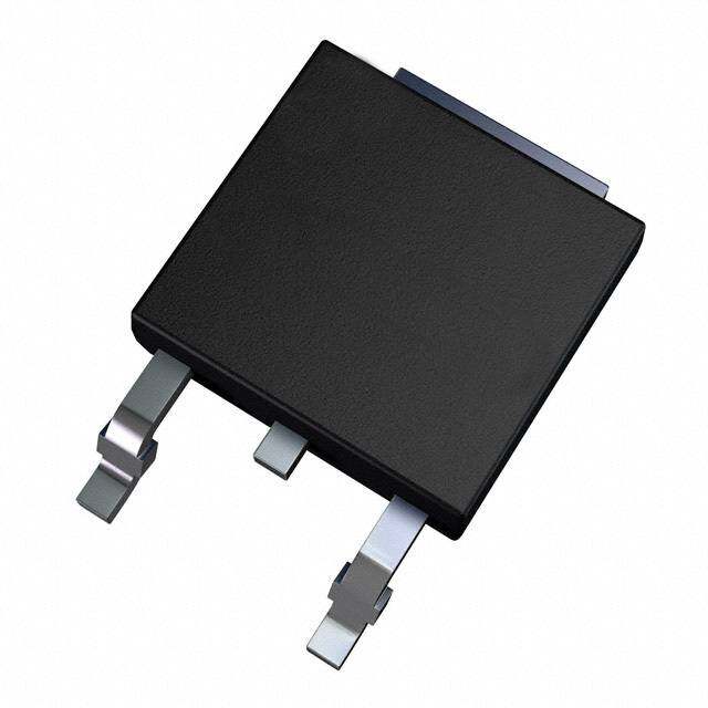
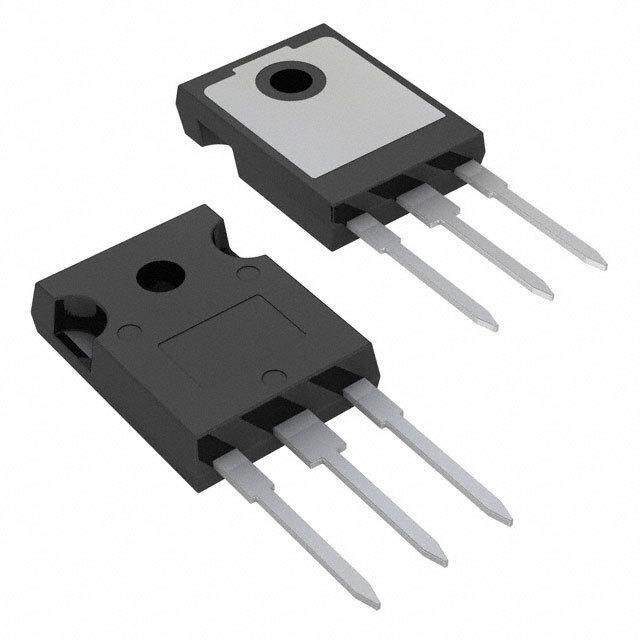
| 产品图片 |
|
| rohs | 符合RoHS无铅 / 符合限制有害物质指令(RoHS)规范要求 |
| 产品系列 | 晶体管,IGBT 晶体管,STMicroelectronics STGW30H65FB- |
| mouser_ship_limit | 该产品可能需要其他文件才能进口到中国。 |
| 数据手册 | |
| 产品型号 | STGW30H65FB |
| SwitchingEnergy | 151µJ (开), 293µJ (关) |
| TestCondition | 400V, 30A, 10 欧姆, 15V |
| 不同 Vge、Ic时的 Vce(on) | 2V @ 15V,30A |
| 产品种类 | IGBT 晶体管 |
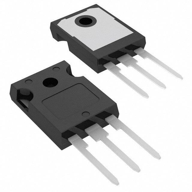
| 供应商器件封装 | TO-247 |
| 其它名称 | 497-14467-5 |
| 功率-最大值 | 260W |
| 功率耗散 | 260 W |
| 包装 | 管件 |
| 反向恢复时间(trr) | - |
| 商标 | STMicroelectronics |
| 在25C的连续集电极电流 | 30 A |
| 安装类型 | 通孔 |
| 安装风格 | Through Hole |
| 封装 | Tube |
| 封装/外壳 | TO-247-3 |
| 封装/箱体 | TO-247-3 |
| 工厂包装数量 | 30 |
| 最大工作温度 | + 175 C |
| 最小工作温度 | - 55 C |
| 栅极/发射极最大电压 | +/- 20 V |
| 栅极—射极漏泄电流 | 250 nA |
| 标准包装 | 30 |
| 特色产品 | http://www.digikey.cn/product-highlights/zh/650-v-igbt-hb-series-transistors/52308 |
| 电压-集射极击穿(最大值) | 650V |
| 电流-集电极(Ic)(最大值) | 30A |
| 系列 | STGW30H65FB |
| 输入类型 | 标准 |
| 配置 | Single |
| 集电极—发射极最大电压VCEO | 650 V |
| 集电极—射极饱和电压 | 1.75 V |
| 集电极最大连续电流Ic | 60 A |


- 商务部:美国ITC正式对集成电路等产品启动337调查
- 曝三星4nm工艺存在良率问题 高通将骁龙8 Gen1或转产台积电
- 太阳诱电将投资9.5亿元在常州建新厂生产MLCC 预计2023年完工
- 英特尔发布欧洲新工厂建设计划 深化IDM 2.0 战略
- 台积电先进制程称霸业界 有大客户加持明年业绩稳了
- 达到5530亿美元!SIA预计今年全球半导体销售额将创下新高
- 英特尔拟将自动驾驶子公司Mobileye上市 估值或超500亿美元
- 三星加码芯片和SET,合并消费电子和移动部门,撤换高东真等 CEO
- 三星电子宣布重大人事变动 还合并消费电子和移动部门
- 海关总署:前11个月进口集成电路产品价值2.52万亿元 增长14.8%


PDF Datasheet 数据手册内容提取
STGFW30H65FB, STGW30H65FB, STGWT30H65FB Trench gate field-stop IGBT, HB series 650 V, 30 A high speed Datasheet - production data Features • Maximum junction temperature: T = 175 °C J 111 • High speed switching series 3 • Minimized tail current 2 1 • V = 1.55 V (typ.) @ I = 30 A TO-3PF CE(sat) C TAB • Tight parameters distribution • Safe paralleling • Low thermal resistance 3 3 2 2 1 1 Applications TO-247 TO-3P • Photovoltaic inverters Figure 1. Internal schematic diagram • High frequency converters C (2, TAB) Description These devices are IGBTs developed using an advanced proprietary trench gate and field stop structure. The device is part of the new HB series G (1) of IGBTs, which represent an optimum compromise between conduction and switching losses to maximize the efficiency of any frequency converter. Furthermore, a slightly positive V temperature coefficient and very CE(sat) tight parameter distribution result in safer E (3) paralleling operation. Table 1. Device summary Order code Marking Package Packing STGFW30H65FB GFW30H65FB TO-3PF Tube STGW30H65FB GW30H65FB TO-247 Tube STGWT30H65FB GWT30H65FB TO-3P Tube July 2015 DocID025849 Rev 5 1/20 This is information on a product in full production. www.st.com 20
Contents STGFW30H65FB, STGW30H65FB, STGWT30H65FB Contents 1 Electrical ratings . . . . . . . . . . . . . . . . . . . . . . . . . . . . . . . . . . . . . . . . . . . . 3 2 Electrical characteristics . . . . . . . . . . . . . . . . . . . . . . . . . . . . . . . . . . . . . 4 2.1 Electrical characteristics (curves) . . . . . . . . . . . . . . . . . . . . . . . . . . . . . . . . 6 3 Test circuits . . . . . . . . . . . . . . . . . . . . . . . . . . . . . . . . . . . . . . . . . . . . . . 12 4 Package information . . . . . . . . . . . . . . . . . . . . . . . . . . . . . . . . . . . . . . . . 13 4.1 TO-3PF package information . . . . . . . . . . . . . . . . . . . . . . . . . . . . . . . . . . 13 4.2 TO-247 package information . . . . . . . . . . . . . . . . . . . . . . . . . . . . . . . . . . 15 4.3 TO-3P package information . . . . . . . . . . . . . . . . . . . . . . . . . . . . . . . . . . . 17 5 Revision history . . . . . . . . . . . . . . . . . . . . . . . . . . . . . . . . . . . . . . . . . . . 19 2/20 DocID025849 Rev 5
STGFW30H65FB, STGW30H65FB, STGWT30H65FB Electrical ratings 1 Electrical ratings Table 2. Absolute maximum ratings Value Unit Symbol Parameter TO-247 TO-3PF TO-3P V Collector-emitter voltage (V = 0) 650 V CES GE I Continuous collector current at T = 25 °C 60 A C C I Continuous collector current at T = 100 °C 30 A C C I (1) Pulsed collector current 120 A CP V Gate-emitter voltage ±20 V GE P Total dissipation at T = 25 °C 260 58 W TOT C Insulation withstand voltage (RMS) from all V three leads to external heat sink (t=1s; 3.5 kV ISO T =25°C) c T Storage temperature range - 55 to 150 °C STG T Operating junction temperature - 55 to 175 °C J 1. Pulse width limited by maximum junction temperature. Table 3. Thermal data Value Symbol Parameter Unit TO-247 TO-3PF TO-3P R Thermal resistance junction-case 2.60 0.58 °C/W thJC R Thermal resistance junction-ambient 50 °C/W thJA DocID025849 Rev 5 3/20
Electrical characteristics STGFW30H65FB, STGW30H65FB, STGWT30H65FB 2 Electrical characteristics T = 25 °C unless otherwise specified. J Table 4. Static characteristics Symbol Parameter Test conditions Min. Typ. Max. Unit Collector-emitter V breakdown voltage I = 2 mA 650 V (BR)CES C (V = 0) GE V = 15 V, I = 30 A 1.55 2 GE C V = 15 V, I = 30 A Collector-emitter saturation GE C 1.65 VCE(sat) voltage TJ = 125 °C V V = 15 V, I = 30 A GE C 1.75 T = 175 °C J V Gate threshold voltage V = V , I = 1 mA 5 6 7 V GE(th) CE GE C Collector cut-off current I V = 650 V 25 µA CES (V = 0) CE GE Gate-emitter leakage I V = ± 20 V 250 nA GES current (V = 0) GE CE Table 5. Dynamic characteristics Symbol Parameter Test conditions Min. Typ. Max. Unit C Input capacitance - 3659 - pF ies C Output capacitance V = 25 V, f = 1 MHz, - 101 - pF oes CE V = 0 Reverse transfer GE C - 76 - pF res capacitance Q Total gate charge - 149 - nC g V = 520 V, I = 30 A, Q Gate-emitter charge CC C - 25 - nC ge V = 15 V, see Figure28 GE Q Gate-collector charge - 62 - nC gc 4/20 DocID025849 Rev 5
STGFW30H65FB, STGW30H65FB, STGWT30H65FB Electrical characteristics Table 6. Switching characteristics (inductive load) Symbol Parameter Test conditions Min. Typ. Max. Unit t Turn-on delay time - 37 - ns d(on) t Current rise time - 14.6 - ns r (di/dt) Turn-on current slope - 1643 - A/µs on V = 400 V, I = 30 A, t Turn-off delay time CE C 146 - ns d(off) R = 10 Ω, V = 15 V, G GE t Current fall time - 23 - ns f see Figure27 E (1) Turn-on switching losses - 151 - µJ on E (2) Turn-off switching losses - 293 - µJ off E Total switching losses - 444 - µJ ts t Turn-on delay time - 35 - ns d(on) t Current rise time - 16.1 - ns r (di/dt) Turn-on current slope - 1496 - A/µs on V = 400 V, I = 30 A, t Turn-off delay time CE C - 158 - ns d(off) R = 10 Ω, V = 15 V, G GE t Current fall time - 65 - ns f T = 175 °C, see Figure27 J E (1) Turn-on switching losses - 175 - µJ on E (2) Turn-off switching losses - 572 - µJ off E Total switching losses - 747 - µJ ts 1. Energy losses include reverse recovery of the external diode. Turn-on times and energy have been measured applying as freewheeling an external SiC diode STPSC206W 2. Turn-off losses include also the tail of the collector current. DocID025849 Rev 5 5/20
Electrical characteristics STGFW30H65FB, STGW30H65FB, STGWT30H65FB 2.1 Electrical characteristics (curves) Figure 2. O utput characteristics (T = 25°C) Figure 3. Output characteristics (T = 175°C) J J GIPG280120141156FSR GIPG280120141206FSR IC IC (A) (A) VGE =15 V 13V VGE =15 V 13V 100 100 11V 11V 9V 9V 80 80 60 60 40 40 20 20 7V 0 0 0 1 2 3 4 VCE(V) 0 1 2 3 4 VCE(V) Figu r e 4. Transfer characteristics Figure 5. Collector current vs. case temperature for TO-247 and TO-3P GIPG280120141330FSR GIPG280120141346FSR IC IC (A) Tj= 25 °C (A) Tj= 175 °C 60 100 VCE =10 V 80 40 60 40 20 20 VGE ≥ 15V, TJ ≤ 175 °C 0 0 7 9 11 13 VGE(V) 0 25 50 75 100 125 150 TC(°C) Figure 6. Collector current vs. case temperature Figure 7. V vs. junction temperature CE(sat) for TO-3PF GIPD060320141418FSR GIPG280120141440FSR IC VCE(sat) (A) (V) VGE= 15V 40 2.2 IC= 60A 30 2.0 1.8 20 1.6 IC= 30A 10 1.4 IC= 15A VGE ≥ 15V, TJ ≤ 175 °C 0 1.2 0 25 50 75 100 125 150 TC(°C) -50 0 50 100 150 TJ(°C) 6/20 DocID025849 Rev 5
STGFW30H65FB, STGW30H65FB, STGWT30H65FB Electrical characteristics Figure 8. Power dissipation vs. case Figure 9. Power dissipation vs. case temperature for TO-247 and TO-3P temperature for TO-3PF GIPG280120141353FSR GIPD060320141444FSR Ptot Ptot (W) (W) 60 250 50 200 40 150 30 100 20 50 10 VGE ≥ 15V, TJ ≤ 175 °C VGE ≥ 15V, TJ ≤ 175 °C 0 0 0 25 50 75 100 125 150 175 TC(°C) 0 25 50 75 100 125 150 TC(°C) Figure 10. F o rward bias safe operating area for Figure 11. Forward bias safe operating area for TO-247 and TO-3P TO-3PF GIPG280120141450FSR GIPD060320141531FSR IC IC (A) (A) 100 100 10 μs 10 μs 10 10 100 μs 100 μs 1 ms 1 ms 1 1 (single pulse TC= 25°C, (single pulse TC= 25°C, TJ ≤ 175°C; VGE=15V) TJ ≤ 175°C; VGE=15V) 0.1 0.1 1 10 100 VCE(V) 1 10 100 VCE(V) Figure 12 . Collector current vs. switching Figure 13. Collector current vs. switching frequency for TO-247 and TO-3P frequency for TO-3PF Ic [A] GIPG280120141713FSR Ic [A] GIPD060320141543FSR 60 Tc=80°C 40 Tc=80°C 50 40 Tc=100°C 30 Tc=100°C 30 20 20 rectangular current shape, 10 rectangular current shape, 10 (duty cycle=0.5, VCC= 400V, RG=10Ω, (duty cycle=0.5, VCC= 400V, RG=10Ω, V = 0/15 V, T=175°C) V = 0/15 V, T=175°C) GE J GE J 0 0 1 10 f [kHz] 1 10 f [kHz] DocID025849 Rev 5 7/20
Electrical characteristics STGFW30H65FB, STGW30H65FB, STGWT30H65FB Figure 14 . Normalized V vs. junction Figure 15. Normalized V vs. junction GE(th) (BR)CES temperature temperature AM16060v1 AM16059v1 VGE(th) V(BR)CES (norm) (norm) VCE= VGE 1.1 IC= 2mA IC= 1mA 1.0 0.9 1.0 0.8 0.7 0.6 0.9 -50 0 50 100 150 TJ(°C) -50 0 50 100 150 TJ(°C) Figure 16. Switching losses vs temperature Figure 17. Switching losses vs gate resistance GIPG280120141531FSR GIPG280120141535FSR E (μJ) E (μJ) VCC= 400V, VGE= 15V VCC= 400V, VGE= 15V Rg= 10Ω, IC= 30A 1020 IC= 30A, TJ= 175 °C EOFF EOFF 600 820 EON 400 620 420 EON 200 220 020 40 60 80 100 120 140 160 TJ(°C) 203 10 17 24 31 38 45RG(Ω) Figure 18. S w itching losses vs collector current Figure 19. Switching losses vs collector emitter voltage GIPG280120141605FSR GIPG280120141609FSR E (μJ) E (μJ) VCC= 400V, VGE= 15V TJ= 175°C, VGE= 15V 1200 Rg= 10Ω, TJ= 175°C Rg= 10Ω, IC= 30A 800 1000 EOFF EOFF 600 800 600 400 EON 400 EON 200 200 0 0 0 20 40 60 IC(A) 150 250 350 450 VCE(V) 8/20 DocID025849 Rev 5
STGFW30H65FB, STGW30H65FB, STGWT30H65FB Electrical characteristics Figure 20. S w itching times vs collector current Figure 21. Switching times vs gate resistance t GIPG100720141533FSR t GIPG100720141549FSR (ns) (ns) TJ= 175°C, VGE= 15V, TJ= 175°C, VGE= 15V, tdoff RG= 10Ω, VCC= 400V IC= 30A, VCC= 400V tdoff 100 tf tdon 100 tdon 10 tr tf tr 1 10 0 10 20 30 40 50 IC(A) 0 10 20 30 40 RG(Ω) Figur e 22. Capacitance variations Figure 23. V vs. collector current CE(sat) C GIPG090720141358FSR VCE(sat) GIPG280120141446FSR (pF) (V) VGE= 15V Cies 2.4 2.2 1000 TJ= 175°C 2.0 1.8 TJ= 25°C 100 1.6 TJ= -40°C Coes 1.4 Cres 10 1.2 0.1 1 10 100 VCE(V) 0 30 45 60 IC(A) Figure 24. G ate charge vs. gate-emitter voltage GIPG280120141455FSR VGE (V) 16 VCC= 520V, IC= 30A IG= 1mA 14 12 10 8 6 4 2 0 0 40 80 120 160 Qg(nC) DocID025849 Rev 5 9/20
Electrical characteristics STGFW30H65FB, STGW30H65FB, STGWT30H65FB Figure 25. Thermal impedance for TO-247 and TO-3P ZthTO2T_B K δ=0.5 0.2 0.1 0.05 -1 10 0.02 Zth=k Rthj-c δ=tp/t 0.01 Single pulse tp t -2 10 10-5 10-4 10-3 10-2 10-1 tp(s) 10/20 DocID025849 Rev 5
STGFW30H65FB, STGW30H65FB, STGWT30H65FB Electrical characteristics Figure 26. Thermal impedance for TO-3PF ZthTOF3T_A K δ=0.5 0.2 0.1 0.05 -1 10 0.02 Zth=k Rthj-c δ=tp/t 0.01 Single pulse tp t -2 10 -5 -4 -3 -2 -1 0 10 10 10 10 10 10 tp(s) DocID025849 Rev 5 11/20
Test circuits STGFW30H65FB, STGW30H65FB, STGWT30H65FB 3 Test circuits Figure 27. Test circuit for inductive load Figure 28. Gate charge test circuit switching k k k k k k AM01504v1 AM01505v1 Figure 29. Switching waveform 90% VG 10% 90% VCE 10% Tr(Voff) Tcross 90% IC TdT(oonn) Tr(Ion) Td(oTofff)f Tf 10% AM01506v1 12/20 DocID025849 Rev 5
STGFW30H65FB, STGW30H65FB, STGWT30H65FB Package information 4 Package information In order to meet environmental requirements, ST offers these devices in different grades of ECOPACK® packages, depending on their level of environmental compliance. ECOPACK® specifications, grade definitions and product status are available at: www.st.com. ECOPACK is an ST trademark. 4.1 TO-3PF package information Figure 30. TO-3PF package outline 7627132_D DocID025849 Rev 5 13/20
Package information STGFW30H65FB, STGW30H65FB, STGWT30H65FB Table 7. TO-3PF package mechanical data mm Dim. Min. Typ. Max. A 5.30 5.70 C 2.80 3.20 D 3.10 3.50 D1 1.80 2.20 E 0.80 1.10 F 0.65 0.95 F2 1.80 2.20 G 10.30 11.50 G1 5.45 H 15.30 15.70 L 9.80 10 10.20 L2 22.80 23.20 L3 26.30 26.70 L4 43.20 44.40 L5 4.30 4.70 L6 24.30 24.70 L7 14.60 15 N 1.80 2.20 R 3.80 4.20 Dia 3.40 3.80 14/20 DocID025849 Rev 5
STGFW30H65FB, STGW30H65FB, STGWT30H65FB Package information 4.2 TO-247 package information Figure 31. TO-247 package outline (cid:19)(cid:19)(cid:26)(cid:24)(cid:22)(cid:21)(cid:24)(cid:66)(cid:43) DocID025849 Rev 5 15/20
Package information STGFW30H65FB, STGW30H65FB, STGWT30H65FB Table 8. TO-247 package mechanical data mm. Dim. Min. Typ. Max. A 4.85 5.15 A1 2.20 2.60 b 1.0 1.40 b1 2.0 2.40 b2 3.0 3.40 c 0.40 0.80 D 19.85 20.15 E 15.45 15.75 e 5.30 5.45 5.60 L 14.20 14.80 L1 3.70 4.30 L2 18.50 ∅P 3.55 3.65 ∅R 4.50 5.50 S 5.30 5.50 5.70 16/20 DocID025849 Rev 5
STGFW30H65FB, STGW30H65FB, STGWT30H65FB Package information 4.3 TO-3P package information Figure 32. TO-3P package outline 8045950_B DocID025849 Rev 5 17/20
Package information STGFW30H65FB, STGW30H65FB, STGWT30H65FB Table 9. TO-3P package mechanical data mm Dim. Min. Typ. Max. A 4.60 4.80 5 A1 1.45 1.50 1.65 A2 1.20 1.40 1.60 b 0.80 1.00 1.20 b1 1.80 2.00 2.20 b2 2.80 3.00 3.20 c 0.55 0.60 0.75 D 19.70 19.90 20.10 D1 13.70 13.90 14.10 E 15.40 15.60 15.80 E1 13.40 13.60 13.80 E2 9.40 9.60 9.90 e 5.15 5.45 5.75 L 19.80 20 20.20 L1 3.30 3.50 3.70 L2 18.20 18.40 18.60 øP 3.30 3.40 3.50 øP1 3.10 3.20 3.30 Q 4.80 5 5.20 Q1 3.60 3.80 4 18/20 DocID025849 Rev 5
STGFW30H65FB, STGW30H65FB, STGWT30H65FB Revision history 5 Revision history Table 10. Document revision history Date Revision Changes 28-Jan-2014 1 Initial release. Updated units in Table6: Switching characteristics (inductive load) for E , and updated note 1. ts Update Figure16: Switching losses vs temperature, Figure17: 24-Feb-2014 2 Switching losses vs gate resistance and Figure18: Switching losses vs collector current. Updated title and features in cover page. Minor text changes. Added device in TO-3PF. Updated Table1: Device summary, Table2: Absolute maximum ratings, Table3: Thermal data. Added Figure6: Collector current vs. case temperature for TO-3PF, 10-Mar-2014 3 Figure9: Power dissipation vs. case temperature for TO-3PF, Figure11: Forward bias safe operating area for TO-3PF and Figure26: Thermal impedance for TO-3PF. Updated Section4: Package information. 20-May-2014 4 Updated Table2: Absolute maximum ratings. Text and formatting changes throughout document Updated Table2: Absolute maximum ratings Updated Section2.1: Electrical characteristics (curves) 28-Jul-2015 5 Updated Section3: Test circuits Updated Section4.2: TO-247 package information Updated Section4.3: TO-3P package information DocID025849 Rev 5 19/20
STGFW30H65FB, STGW30H65FB, STGWT30H65FB IMPORTANT NOTICE – PLEASE READ CAREFULLY STMicroelectronics NV and its subsidiaries (“ST”) reserve the right to make changes, corrections, enhancements, modifications, and improvements to ST products and/or to this document at any time without notice. Purchasers should obtain the latest relevant information on ST products before placing orders. ST products are sold pursuant to ST’s terms and conditions of sale in place at the time of order acknowledgement. Purchasers are solely responsible for the choice, selection, and use of ST products and ST assumes no liability for application assistance or the design of Purchasers’ products. No license, express or implied, to any intellectual property right is granted by ST herein. Resale of ST products with provisions different from the information set forth herein shall void any warranty granted by ST for such product. ST and the ST logo are trademarks of ST. All other product or service names are the property of their respective owners. Information in this document supersedes and replaces information previously supplied in any prior versions of this document. © 2015 STMicroelectronics – All rights reserved 20/20 DocID025849 Rev 5