ICGOO在线商城 > 分立半导体产品 > 晶体管 - 双极 (BJT) - 射频 > NE85634-T1-A
 Datasheet下载
- 型号: NE85634-T1-A
- 制造商: CEL
- 库位|库存: xxxx|xxxx
- 要求:
| 数量阶梯 | 香港交货 | 国内含税 |
| +xxxx | $xxxx | ¥xxxx |
查看当月历史价格
查看今年历史价格
NE85634-T1-A产品简介:
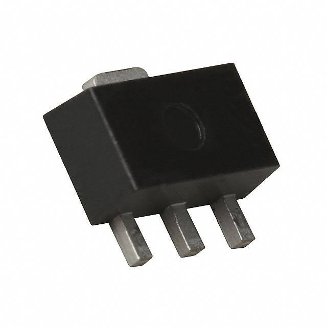
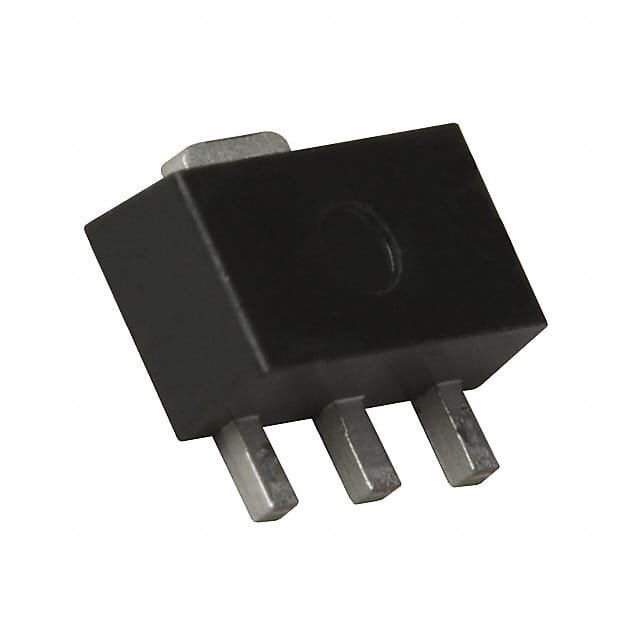
ICGOO电子元器件商城为您提供NE85634-T1-A由CEL设计生产,在icgoo商城现货销售,并且可以通过原厂、代理商等渠道进行代购。 NE85634-T1-A价格参考。CELNE85634-T1-A封装/规格:晶体管 - 双极 (BJT) - 射频, RF Transistor NPN 12V 100mA 6.5GHz 2W Surface Mount SOT-89。您可以下载NE85634-T1-A参考资料、Datasheet数据手册功能说明书,资料中有NE85634-T1-A 详细功能的应用电路图电压和使用方法及教程。
CEL NE85634-T1-A是一款双极结型晶体管(BJT),专门用于射频(RF)应用。其主要应用场景包括:

1. 射频放大器:该器件适用于构建高频放大电路,广泛用于无线通信系统中的信号增强,如蜂窝基站、无线接入点和广播设备。

2. 频率转换电路:可在混频器或变频器中使用,用于将信号从一个频率转换到另一个频率,常见于通信设备和雷达系统中。

3. 射频驱动器和前置放大器:由于其良好的高频特性和增益表现,适用于射频发射链中的驱动级或接收链中的前置放大电路。

4. 测试与测量设备:在射频测试仪器中作为关键放大元件,用于信号处理和测试分析。

5. 工业与通信基础设施:如微波通信、卫星通信、光纤通信系统中,作为高频信号处理的核心元件。

该晶体管采用SOT-23封装,适合高频率、低噪声和中等功率的应用场景,具备良好的稳定性和可靠性,适用于工业级工作环境。
| 参数 | 数值 |
| 产品目录 | |
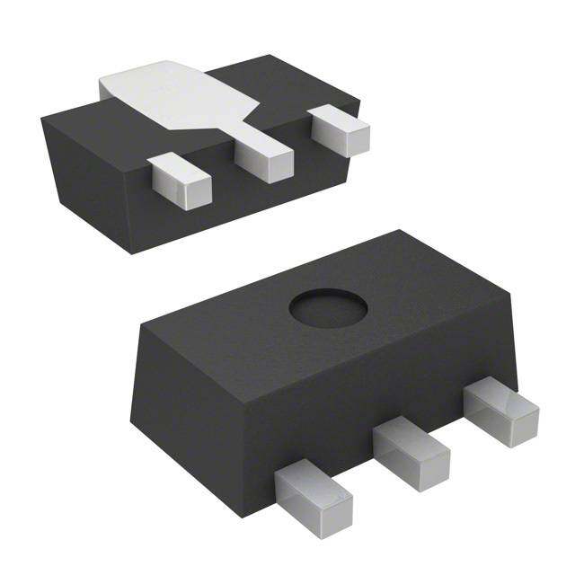
| 描述 | TRANSISTOR NPN 1GHZ SOT-89 |
| 产品分类 | RF 晶体管 (BJT) |
| 品牌 | CEL |
| 数据手册 | |
| 产品图片 |
|
| 产品型号 | NE85634-T1-A |
| rohs | 无铅 / 符合限制有害物质指令(RoHS)规范要求 |
| 产品系列 | - |
| 不同 Ic、Vce 时的DC电流增益(hFE)(最小值) | 50 @ 20mA,10V |
| 产品目录页面 | |
| 供应商器件封装 | SOT-89 |
| 其它名称 | NE85634-ACT |
| 功率-最大值 | 2W |
| 包装 | 剪切带 (CT) |
| 噪声系数(dB,不同f时的典型值) | 1.4dB @ 1GHz |
| 增益 | - |
| 安装类型 | 表面贴装 |
| 封装/外壳 | TO-243AA |
| 晶体管类型 | NPN |
| 标准包装 | 1 |
| 电压-集射极击穿(最大值) | 12V |
| 电流-集电极(Ic)(最大值) | 100mA |
| 频率-跃迁 | 6.5GHz |


- 商务部:美国ITC正式对集成电路等产品启动337调查
- 曝三星4nm工艺存在良率问题 高通将骁龙8 Gen1或转产台积电
- 太阳诱电将投资9.5亿元在常州建新厂生产MLCC 预计2023年完工
- 英特尔发布欧洲新工厂建设计划 深化IDM 2.0 战略
- 台积电先进制程称霸业界 有大客户加持明年业绩稳了
- 达到5530亿美元!SIA预计今年全球半导体销售额将创下新高
- 英特尔拟将自动驾驶子公司Mobileye上市 估值或超500亿美元
- 三星加码芯片和SET,合并消费电子和移动部门,撤换高东真等 CEO
- 三星电子宣布重大人事变动 还合并消费电子和移动部门
- 海关总署:前11个月进口集成电路产品价值2.52万亿元 增长14.8%


PDF Datasheet 数据手册内容提取
DATA SHEET NPN SILICON RF TRANSISTOR 2SC3357 NE85634 / JEITA Part No. T NPN EPITAXIAL SILICON RF TRANSISTOR FOR HIGH-FREQUENCY LOW-NOISE AMPLIFICATION 3-PIN POWER MINIMOLD U FEATURES • Low noise and high gain NF = 1.1 dB TYP., Ga = 7.5 dB TYP. @ VCE = 10 V, IC = 7 mA, f = 1 GHz O NF = 1.8 dB TYP., Ga = 9.0 dB TYP. @ VCE = 10 V, IC = 40 mA, f = 1 GHz • High power gain : MAG = 10 dB TYP. @ IC = 40 mA, f = 1 GHz • Large Ptot : Ptot = 1.2 W (Mounted on 16 cm2 · 0.7 mm (t) ceramic substrate) • Small package : 3-pin power minimold package - ORDERING INFORMATION E Part Number Quantity Supplying Form NE85634-A 25 pcs (Non reel) •12 mm wide embossed taping 2SC3357-A •Collector face the perforation side of the tape NE85634-T1-A 1 kpcs/reel 2SC3357-T1-A S Remark To order evaluation samples, contact your nearby sales office. The unit sample quantity is 25 pcs. A ABSOLUTE MAXIMUM RATINGS (TA = +25(cid:176) (cid:176)(cid:176)(cid:176) C) Parameter Symbol Ratings Unit Collector to Base Voltage VCBO 20 V H Collector to Emitter Voltage VCEO 12 V Emitter to Base Voltage VEBO 3.0 V Collector Current IC 100 mA Total Power Dissipation Ptot Note 1.2 W P Junction Temperature Tj 150 (cid:176) C Storage Temperature Tstg - 65 to +150 (cid:176) C Note Mounted on 16 cm2 · 0.7 mm (t) ceramic substrate Caution Observe precautions when handling because these devices are sensitive to electrostatic discharge. The information in this document is subject to change without notice. Before using this document, please confirm that this is the latest version. Document No. PU10211EJ01V0DS (1st edition) The mark (cid:144)(cid:144)(cid:144)(cid:144) shows major revised points. (Previous No. P10357EJ4V1DS00) Date Published January 2003 CP(K)
NE85634 / 2SC3357 THERMAL RESISTANCE Parameter Symbol Value Unit Junction to Ambient Resistance Rth (j-a)Note 62.5 °C/W T Note Mounted on 16 cm2× 0.7 mm (t) ceramic substrate ELECTRICAL CHARACTERISTICS (TA = +25°°°°C) U Parameter Symbol Test Conditions MIN. TYP. MAX. Unit DC Characteristics Collector Cut-off Current ICBO VCB = 10 V, IE = 0 mA – – 1.0 μA Emitter Cut-off Current IEBO VEB = 1.0 V, IC = 0 mA O– – 1.0 μA DC Current Gain hFE Note 1 VCE = 10 V, IC = 20 mA 50 120 250 – RF Characteristics Gain Bandwidth Product fT VCE = 10 V, IC = 20 mA – 6.5 – GHz Insertion Power Gain ⏐S21e⏐2 VCE = 10 V, IC = 20 mA, f =- 1 GHz – 9.0 – dB Noise Figure (1) NF VCE = 10 V, IC = 7 mA, f = 1 GHz – 1.1 – dB E Noise Figure (2) NF VCE = 10 V, IC = 40 mA, f = 1 GHz – 1.8 3.0 dB Reverse Transfer Capacitance CreNote 2 VCB = 10 V, IE = 0 mA, f = 1 MHz – 0.65 1.0 pF Notes 1. Pulse measurement: PW ≤ 350 μs, Duty Cycle ≤ 2% S 2. The emitter terminal and the case shall be connected to the guard terminal of the three-terminal capacitance bridge. hFE CLASSIFICATION A Rank RH RF RE Marking RH RF RE hFE Value 50 to 100 80 to 160 125 to 250 H P 2 Data Sheet PU10211EJ01V0DS
NE85634 / 2SC3357 TYPICAL CHARACTERISTICS (TA = +25°°°°C, unless otherwise specified) TOTAL POWER DISSIPATION REVERSE TRANSFER CAPACITANCE vs. AMBIENT TEMPERATURE vs. COLLECTOR TO BASE VOLTAGE pF) 2 Tf = 1 MHz n P (W)tot 2 ance C (re patio C16e rcamm2ic× s0u.7b smtrmat e(t) pacit 1 U si a s C er Di 1 sfer w n Po Tra 0.5 al Free air Rth (j-a) 312.5˚C/W e Tot ers O v e R 0.3 0 25 50 75 100 125 150 0.2 0.5 1 2 5 10 20 30 Ambient Temperature TA (˚C) Collector to Base Voltage VCB (V) DC CURRENT GAIN vs. GAIN BANDWIDTH PRODUCT - COLLECTOR CURRENT vs. COLLECTOR CURRENT 200 10 VCE = 10 V Ez) VCE = 10 V H 5 G ain hFE 100 duct f (T 32 G o ent 50 S h Pr 1 C Curr ndwidt 0.5 D a 20 B 0.3 n ai 0.2 A G 10 0.1 0.5 1 5 10 50 0.1 0.5 1 5 10 50 100 Collector Current IC (mA) Collector Current IC (mA) INSERTION POWER GAIN, MAG INSERTION POWER GAIN H vs. FREQUENCY vs. COLLECTOR CURRENT B) 25 15 2S| (dB)21ewer Gain MAG (d 1250P |S21eM|2AG 2| (dB)ain |S21e 10 Vf =CE 1 = G 1H0z V ertion Power Gain |ximum Available Po 150 IVCC =E =2 01 0m VA Insertion Power G 5 nsMa 0 0 I 0.05 0.1 0.2 0.5 1 2 0.5 1 5 10 5070 Frequency f (GHz) Collector Current IC (mA) Data Sheet PU10211EJ01V0DS 3
NE85634 / 2SC3357 NOISE FIGURE vs. 7 COLLECTOR CURRENVf =CTE 1 = G 1H0z V M (dBc)2M (dBc)3 100 IM2, IM3 vs. COLVVLCoEE= C= 1 10T00O VdRBμ VC/5U0R ΩRENT NF (dB) 56 Distortion IDistortion I 9800 IIRMMg 23=:: ffR ==e =92 0 5× 0+ 2 Ω10000 – M I1MTH930z MHz Noise Figure 1234 Order Intermodulation Order Intermodulation 76450000 U IM2 00.5 1 5 10 5070 2nd 3rd 30 20 O30 40 50 60 70 Collector Current IC (mA) Collector Current IC (mA) Remark The graphs indicate nominal characteristics. - S-PARAMETERS E S A H P 4 Data Sheet PU10211EJ01V0DS
NE85634 / 2SC3357 SMITH CHART S11e, S22e-FREQUENCY CONDITION : VCE = 10 V WAVELENG0T904H..00S1TO804W..00A2R0D100..409G704E2..00ND.00A.O40EL38DRRAWAOITNCCEOLOEF3TFEFRTC060IFE.OSON.E40HT40LI.RTG7N.NG00DANE40GE6R4L1−0EE001E.V0.S0A45.W.60401..000255501.100−.05.20.045440.3.T000.1N6.P00E0O.6N004SIO1.3T.1IP404−VME 0O4RC3E EA40CC4.NT.7. 0AA00(0 ).+ T N00X J–4C7 .–0C –XJ .A− –E–403EZ––0.2)1CRO3O–1Z(O3 − E 2M V0 PI4 0T5.O8A..00GN.00005EE.8.NN04T0.30221112−0496.0.00.0.0006..940.401 f000 10714.00.0.=710.511.1.0−.040R0 0E0AC0.6.T9A80210.0.803N.01.1.CS 1300.70.E10G091 0C−1 00.8.O9 9 .01 H( M e– 8 20P0–RZ3O–O1z..0.91–3N..0)02E8N01.00.1.019T90−2020..030470.2.002..14.3.1.200341.6..0.0740.03.6060..0861.402..18.0E1.0208.Sf8.00848 0006.01.1−.=1.331.6.21011..60.0240 e21.84.110.042.050.f51307 .f 31.570G =0-.5−0=6 .11.H6 0026.0z3.14..3.04.21380.601.16.0800 6 G−00G.4.0722..3001H.33.1H03.70z5.050z0058.−310.22.013.800.033.409.0304110.10−01.130.9.4040.O0.02030230.006.3050.−00.23.00100.122.1092005202005−00209.0222..1012201.080−00.320287..022.2004.22.6052.007.22.3006.22.4052.0 U:: IICC == 2400 mmAAT S S21e-FREQUENCY S12e-FREQUENCY CONDITION : VCE = 10 V, IC = 20 mA CONDITION : VCE = 10 V, IC = 20 mA 90˚ A 90˚ 120˚ f = 0.2 GHz 60˚ 120˚ 60˚ f = 2.0 GHz S21e 150˚ 30˚ 150˚ 30˚ H S12e f = 2.0 GHz f = 0.2 GHz 180˚ 0˚ 180˚ 0˚ 3 6 9 12 15 0.1 0.2 0.3 0.4 0.5 P –150˚ –30˚ –150˚ –30˚ –120˚ –60˚ –120˚ –60˚ –90˚ –90˚ Data Sheet PU10211EJ01V0DS 5
NE85634 / 2SC3357 PACKAGE DIMENSIONS 3-PIN POWER MINIMOLD (UNIT: mm) 4.5±0.1 T 1.6±0.2 1.5±0.1 E C B 2.5±0.1 4.0±0.25 U N. MI 8 0. 0.42±0.06 0.42±0.06 0.O41+–00..0036 0.47±0.06 1.5 3.0 - PIN CONNECTIONS E: Emitter E C: Collector (Fin) B: Base (IEC : SOT-89) S A H P 6 Data Sheet PU10211EJ01V0DS
NOTICE 1. Descriptions of circuits, software and other related information in this document are provided only to illustrate the operation of semiconductor products and application examples. You are fully responsible for the incorporation of these circuits, software, and information in the design of your equipment. California Eastern Laboratories and Renesas Electronics assumes no responsibility for any losses incurred by you or third parties arising from the use of these circuits, software, or information. T 2. California Eastern Laboratories has used reasonable care in preparing the information included in this document, but California Eastern Laboratories does not warrant that such information is error free. California Eastern Laboratories and Renesas Electronics assumes no liability whatsoever for any damages incurred by you resulting from errors in or omissions from the information included herein. 3. California Eastern Laboratories and Renesas Electronics do not assume any liability for infringement of patents, copyrights, or other intellectual property rights of third parties by or arising from the use of Renesas Electronics products or technical information described in this document. No license, express, U implied or otherwise, is granted hereby under any patents, copyrights or other intellectual property rights of California Eastern Laboratories or Renesas Electronics or others. 4. You should not alter, modify, copy, or otherwise misappropriate any Renesas Electronics product, whether in whole or in part. California Eastern Laboratories and Renesas Electronics assume no responsibility for any losses incurred by you or third parties arising from such alteration, modification, copy or otherwise misappropriation of Renesas Electronics product. 5. Renesas Electronics products are classified according to the following two quality grades: “Standard” and “High Quality”. The recommended applications for each Renesas Electronics product depends on the product’s quality grade, as indicated below. “Standard”: Computers; office equipment; communications O equipment; test and measurement equipment; audio and visual equipment; home electronic appliances; machine tools; personal electronic equipment; and industrial robots etc. “High Quality”: Transportation equipment (automobiles, trains, ships, etc.); traffic control systems; anti-disaster systems; anti-crime systems; and safety equipment etc. Renesas Electronics products are neither intended nor authorized for use in products or systems that may pose a direct threat to human life or bodily injury (artificial life support devices or systems, surgical implantations etc.), or may cause serious property damages (nuclear reactor control systems, military equipment etc.). You must check the quality grade of each Renesas Electronics product before using it in a particular application. You may not use any Renesas Electronics product for any application for which it is not intended. California Eastern Laboratories and Renesas Electronics shall not be in any way liable for any damages or losses incurred by you or third parties arising from the use of any Renesas Electronics product for which the product is not intended by California Eastern Laboratories or Renesas Elec-tronics. 6. You should use the Renesas Electronics products described in this document within the range specified by California Eastern Laboratories, especially with respect to the maximum rating, operating supply voltage range, movement power voltage range, heat radiation characteristics, installation and other product characteristics. California Eastern Laboratories shall have no liability for malfunEctions or damages arising out of the use of Renesas Electronics products beyond such specified ranges. 7. Although Renesas Electronics endeavors to improve the quality and reliability of its products, semiconductor products have specific characteristics such as the occurrence of failure at a certain rate and malfunctions under certain use conditions. Further, Renesas Electronics products are not subject to radiation resistance design. Please be sure to implement safety measures to guard them against the possibility of physical injury, and injury or damage caused by fire in the event of the failure of a Renesas Electronics product, such as safety design for hardware and software including but not limited to redundancy, fire control and malfunction prevention, appropriate treatment for aging degradation or any other appropriate measures. Because the evaluation of S microcomputer software alone is very difficult, please evaluate the safety of the final products or systems manufactured by you. 8. Please contact a California Eastern Laboratories sales office for details as to environmental matters such as the environmental compatibility of each Renesas Electronics product. Please use Renesas Electronics products in compliance with all applicable laws and regulations that regulate the inclusion or use of controlled substances, including without limitation, the EU RoHS Directive. California Eastern Laboratories and Renesas Electronics assume no liability for damages or losses occurring as a result of your noncompliance with applicable laws and regulations. 9. Renesas Electronics products and technology may not be used for or incorporated into any products or systems whose manufacture, use, or sale is prohibited under any applicable domestic or foreign laws oAr regulations. You should not use Renesas Electronics products or technology described in this document for any purpose relating to military applications or use by the military, including but not limited to the development of weapons of mass destruction. When exporting the Renesas Electronics products or technology described in this document, you should comply with the applicable export control laws and regulations and follow the procedures required by such laws and regulations. 10. It is the responsibility of the buyer or distributor of California Eastern Laboratories, who distributes, disposes of, or otherwise places the Renesas Electronics product with a third party, to notify such third party in advance of the contents and conditions set forth in this document, California Eastern Laboratories and Renesas Electronics assume no responsibility for any losses incurred by you or third parties as a result of unauthorized use of Renesas Electronics products. H 11. This document may not be reproduced or duplicated in any form, in whole or in part, without prior written consent of California Eastern Laboratories. 12. Please contact a California Eastern Laboratories sales office if you have any questions regarding the information contained in this document or Renesas Electronics products, or if you have any other inquiries. NOTE 1: “Renesas Electronics” as used in this document means Renesas Electronics Corporation and also includes its majority-owned subsidiaries. NOTE 2: “Renesas Electronics product(s)” means any product developed or manufactured by or for Renesas Electronics. NOTE 3: Products and product information are subject to change without notice. P CEL Headquarters • 4590 Patrick Henry Drive, Santa Clara, CA 95054 • Phone (408) 919-2500 • www.cel.com For a complete list of sales offices, representatives and distributors, Please visit our website: www.cel.com/contactus