ICGOO在线商城 > 分立半导体产品 > 晶体管 - FET,MOSFET - 单 > FDP8896
 Datasheet下载
- 型号: FDP8896
- 制造商: Fairchild Semiconductor
- 库位|库存: xxxx|xxxx
- 要求:
| 数量阶梯 | 香港交货 | 国内含税 |
| +xxxx | $xxxx | ¥xxxx |
查看当月历史价格
查看今年历史价格
FDP8896产品简介:
ICGOO电子元器件商城为您提供FDP8896由Fairchild Semiconductor设计生产,在icgoo商城现货销售,并且可以通过原厂、代理商等渠道进行代购。 FDP8896价格参考。Fairchild SemiconductorFDP8896封装/规格:晶体管 - FET,MOSFET - 单, 通孔 N 沟道 30V 16A(Ta),92A(Tc) 80W(Tc) TO-220-3。您可以下载FDP8896参考资料、Datasheet数据手册功能说明书,资料中有FDP8896 详细功能的应用电路图电压和使用方法及教程。
ON Semiconductor(安森美半导体)的FDP8896是一款N沟道MOSFET,属于晶体管 - FET、MOSFET - 单类别。其主要应用场景包括:

1. 开关电源(SMPS):FDP8896具有低导通电阻(Rds(on)),使其非常适合用于高效能的开关电源设计中,能够减少功率损耗并提高转换效率。

2. 电机控制:该MOSFET可用于各种电机驱动应用,如直流无刷电机(BLDC)或步进电机控制。其快速开关特性和低导通电阻有助于实现高效的电机速度和方向控制。

3. 负载开关:在需要动态管理电路中不同负载的应用中,FDP8896可以用作负载开关,提供快速响应和低功耗特性,适用于消费电子、工业设备等。

4. 电池管理:在电池供电系统中,这款MOSFET可以作为电池保护或充放电控制的关键元件,确保电池的安全运行和延长使用寿命。

5. 逆变器和转换器:FDP8896适用于太阳能逆变器和其他类型的电力转换设备,支持高效的能量转换过程,降低热损耗。

6. 汽车电子:在汽车领域,此型号可用于车身控制系统、启动/停止系统以及电动助力转向等应用中,满足严格的车规级要求。

总之,FDP8896凭借其高性能参数和可靠性,广泛应用于消费类电子产品、工业自动化、通信基础设施以及汽车电子等多个领域,特别是在需要高效率、低功耗及快速切换能力的设计中表现出色。
| 参数 | 数值 |
| 产品目录 | |
| ChannelMode | Enhancement |
| 描述 | MOSFET N-CH 30V 92A TO-220ABMOSFET 30V N-Channel PowerTrench |
| 产品分类 | FET - 单分离式半导体 |
| FET功能 | 逻辑电平门 |
| FET类型 | MOSFET N 通道,金属氧化物 |
| Id-ContinuousDrainCurrent | 92 A |
| Id-连续漏极电流 | 92 A |
| 品牌 | Fairchild Semiconductor |
| 产品手册 | |
| 产品图片 |
|
| rohs | 符合RoHS无铅 / 符合限制有害物质指令(RoHS)规范要求 |
| 产品系列 | 晶体管,MOSFET,Fairchild Semiconductor FDP8896PowerTrench® |
| 数据手册 | |
| 产品型号 | FDP8896 |
| PCN封装 | |
| Pd-PowerDissipation | 80 W |
| Pd-功率耗散 | 80 W |
| RdsOn-Drain-SourceResistance | 59 mOhms |
| RdsOn-漏源导通电阻 | 59 mOhms |
| Vds-Drain-SourceBreakdownVoltage | 30 V |
| Vds-漏源极击穿电压 | 30 V |
| Vgs-Gate-SourceBreakdownVoltage | +/- 20 V |
| Vgs-栅源极击穿电压 | 20 V |
| 上升时间 | 103 ns |
| 下降时间 | 44 ns |
| 不同Id时的Vgs(th)(最大值) | 2.5V @ 250µA |
| 不同Vds时的输入电容(Ciss) | 2525pF @ 15V |
| 不同Vgs时的栅极电荷(Qg) | 67nC @ 10V |
| 不同 Id、Vgs时的 RdsOn(最大值) | 5.9 毫欧 @ 35A,10V |
| 产品培训模块 | http://www.digikey.cn/PTM/IndividualPTM.page?site=cn&lang=zhs&ptm=356 |
| 产品种类 | MOSFET |
| 供应商器件封装 | TO-220AB |
| 典型关闭延迟时间 | 56 ns |
| 功率-最大值 | 80W |
| 包装 | 管件 |
| 单位重量 | 1.800 g |
| 商标 | Fairchild Semiconductor |
| 安装类型 | 通孔 |
| 安装风格 | Through Hole |
| 封装 | Tube |
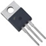
| 封装/外壳 | TO-220-3 |
| 封装/箱体 | TO-220-3 |
| 工厂包装数量 | 50 |
| 晶体管极性 | N-Channel |
| 最大工作温度 | + 175 C |
| 最小工作温度 | - 55 C |
| 标准包装 | 50 |
| 漏源极电压(Vdss) | 30V |
| 电流-连续漏极(Id)(25°C时) | 16A (Ta), 92A (Tc) |
| 系列 | FDP8896 |
| 通道模式 | Enhancement |
| 配置 | Single |
| 零件号别名 | FDP8896_NL |


PDF Datasheet 数据手册内容提取
Is Now Part of To learn more about ON Semiconductor, please visit our website at www.onsemi.com Please note: As part of the Fairchild Semiconductor integration, some of the Fairchild orderable part numbers will need to change in order to meet ON Semiconductor’s system requirements. Since the ON Semiconductor product management systems do not have the ability to manage part nomenclature that utilizes an underscore (_), the underscore (_) in the Fairchild part numbers will be changed to a dash (-). This document may contain device numbers with an underscore (_). Please check the ON Semiconductor website to verify the updated device numbers. The most current and up-to-date ordering information can be found at www.onsemi.com. Please email any questions regarding the system integration to Fairchild_questions@onsemi.com. ON Semiconductor and the ON Semiconductor logo are trademarks of Semiconductor Components Industries, LLC dba ON Semiconductor or its subsidiaries in the United States and/or other countries. ON Semiconductor owns the rights to a number of patents, trademarks, copyrights, trade secrets, and other intellectual property. A listing of ON Semiconductor’s product/patent coverage may be accessed at www.onsemi.com/site/pdf/Patent-Marking.pdf. ON Semiconductor reserves the right to make changes without further notice to any products herein. ON Semiconductor makes no warranty, representation or guarantee regarding the suitability of its products for any particular purpose, nor does ON Semiconductor assume any liability arising out of the application or use of any product or circuit, and specifically disclaims any and all liability, including without limitation special, consequential or incidental damages. Buyer is responsible for its products and applications using ON Semiconductor products, including compliance with all laws, regulations and safety requirements or standards, regardless of any support or applications information provided by ON Semiconductor. “Typical” parameters which may be provided in ON Semiconductor data sheets and/or specifications can and do vary in different applications and actual performance may vary over time. All operating parameters, including “Typicals” must be validated for each customer application by customer’s technical experts. ON Semiconductor does not convey any license under its patent rights nor the rights of others. ON Semiconductor products are not designed, intended, or authorized for use as a critical component in life support systems or any FDA Class 3 medical devices or medical devices with a same or similar classification in a foreign jurisdiction or any devices intended for implantation in the human body. Should Buyer purchase or use ON Semiconductor products for any such unintended or unauthorized application, Buyer shall indemnify and hold ON Semiconductor and its officers, employees, subsidiaries, affiliates, and distributors harmless against all claims, costs, damages, and expenses, and reasonable attorney fees arising out of, directly or indirectly, any claim of personal injury or death associated with such unintended or unauthorized use, even if such claim alleges that ON Semiconductor was negligent regarding the design or manufacture of the part. ON Semiconductor is an Equal Opportunity/Affirmative Action Employer. This literature is subject to all applicable copyright laws and is not for resale in any manner.
F D N P 8 8 May 2008 9 6 FDP8896 tmM N-Channel PowerTrench® MOSFET 30V, 92A, 5.9mΩ General Description Features This N-Channel MOSFET has been designed specifically to (cid:127) r = 5.9mΩ, V = 10V, I = 35A DS(ON) GS D improve the overall efficiency of DC/DC converters using either synchronous or conventional switching PWM (cid:127) rDS(ON) = 7.0mΩ, VGS = 4.5V, ID = 35A controllers. It has been optimized for low gate charge, low r and fast switching speed. (cid:127) High performance trench technology for extremely low DS(ON) r DS(ON) (cid:127) Low gate charge Applications (cid:127) High power and current handling capability • DC/DC converters • RoHS Compliant (FLANGE) D DRAIN SOURCE DRAIN GATE G TO-220AB S FDP SERIES MOSFET Maximum Ratings TC = 25°C unless otherwise noted Symbol Parameter Ratings Units V Drain to Source Voltage 30 V DSS V Gate to Source Voltage ±20 V GS Drain Current Continuous (T = 25oC, V = 10V) (Note 1) 92 A C GS I Continuous (T = 25oC, V = 4.5V) (Note 1) 85 A D C GS Continuous (Tamb = 25oC, VGS = 10V, with RθJA = 62oC/W) 16 A Pulsed Figure 4 A E Single Pulse Avalanche Energy (Note 2) 74 mJ AS Power dissipation 80 W P D Derate above 25oC 0.53 W/oC T , T Operating and Storage Temperature -55 to 175 oC J STG Thermal Characteristics RθJC Thermal Resistance Junction to Case TO-220 1.88 oC/W RθJA Thermal Resistance Junction to Ambient TO-220 ( Note 3) 62 oC/W Package Marking and Ordering Information Device Marking Device Package Reel Size Tape Width Quantity FDP8896 FDP8896 TO-220AB Tube N/A 50 units ©2008 Fairchild Semiconductor Corporation FDP8896 Rev. A2
F Electrical Characteristics T = 25°C unless otherwise noted D C P Symbol Parameter Test Conditions Min Typ Max Units 8 8 Off Characteristics 9 6 B Drain to Source Breakdown Voltage I = 250µA, V = 0V 30 - - V VDSS D GS V = 24V - - 1 I Zero Gate Voltage Drain Current DS µA DSS V = 0V T = 150oC - - 250 GS C I Gate to Source Leakage Current V = ±20V - - ±100 nA GSS GS On Characteristics V Gate to Source Threshold Voltage V = V , I = 250µA 1.2 - 2.5 V GS(TH) GS DS D I = 35A, V = 10V - 0.0050 0.0059 D GS I = 35A, V = 4.5V - 0.0060 0.0070 r Drain to Source On Resistance D GS Ω DS(ON) I = 35A, V = 10V, D GS - 0.0078 0.0094 T = 175oC J Dynamic Characteristics C Input Capacitance - 2525 - pF ISS V = 15V, V = 0V, C Output Capacitance DS GS - 490 - pF OSS f = 1MHz C Reverse Transfer Capacitance - 300 - pF RSS R Gate Resistance V = 0.5V, f = 1MHz - 2.3 - Ω G GS Q Total Gate Charge at 10V V = 0V to 10V - 48 67 nC g(TOT) GS Q Total Gate Charge at 5V V = 0V to 5V - 25 36 nC g(5) GS V = 15V Q Threshold Gate Charge V = 0V to 1V DD - 2.3 3.0 nC g(TH) GS I = 35A Q Gate to Source Gate Charge D - 8 - nC gs I = 1.0mA g Q Gate Charge Threshold to Plateau - 5.7 - nC gs2 Q Gate to Drain “Miller” Charge - 9.5 - nC gd Switching Characteristics (V = 10V) GS t Turn-On Time - - 168 ns ON t Turn-On Delay Time - 9 - ns d(ON) tr Rise Time VDD = 15V, ID = 35A - 103 - ns td(OFF) Turn-Off Delay Time VGS = 4.5V, RGS = 6.2Ω - 56 - ns t Fall Time - 44 - ns f t Turn-Off Time - - 150 ns OFF Drain-Source Diode Characteristics I = 35A - - 1.25 V V Source to Drain Diode Voltage SD SD I = 20A - - 1.0 V SD t Reverse Recovery Time I = 35A, dI /dt = 100A/µs - - 27 ns rr SD SD Q Reverse Recovered Charge I = 35A, dI /dt = 100A/µs - - 12 nC RR SD SD Notes: 1: Package current limitation is 80A. 2: Starting TJ = 25°C, L = 36µH, IAS = 64A, VDD = 27V, VGS = 10V. 3: Pulse width = 100s. 4 ©2008 Fairchild Semiconductor Corporation FDP8896 Rev. A2
F Typical Characteristics D T = 25°C unless otherwise noted C P 8 1.2 8 100 9 CURRENT LIMITED 6 R 1.0 BY PACKAGE LIE 80 ULTIP 0.8 NT (A) VGS = 10V SSIPATION M 00..46 RAIN CURRE 4600 VGS = 4.5V DI D R , D WE 0.2 I 20 O P 0 0 0 25 50 75 100 125 150 175 25 50 75 100 125 150 175 TC, CASE TEMPERATURE (oC) TC, CASE TEMPERATURE (oC) Figure 1. Normalized Power Dissipation vs Case Figure 2. Maximum Continuous Drain Current vs Temperature Case Temperature 2 DUTY CYCLE - DESCENDING ORDER 1 0.5 0.2 0.1 0.05 E DC 0.02 ZEAN 0.01 ORMALIL IMPED 0.1 PDM NA Z, θJCTHERM t1t2 NOTES: DUTY FACTOR: D = t1/t2 SINGLE PULSE PEAK TJ = PDM x ZθJC x RθJC + TC 0.01 10-5 10-4 10-3 10-2 10-1 100 101 t, RECTANGULAR PULSE DURATION (s) Figure 3. Normalized Maximum Transient Thermal Impedance 1000 TC = 25oC FOR TEMPERATURES TRANSCONDUCTANCE MAY LIMIT CURRENT ABOVE 25oC DERATE PEAK A) IN THIS REGION CURRENT AS FOLLOWS: T ( REN I = I25 175 - TC UR VGS = 4.5V 150 C K A E P , M D I 100 50 10-5 10-4 10-3 10-2 10-1 100 101 t, PULSE WIDTH (s) Figure 4. Peak Current Capability ©2008 Fairchild Semiconductor Corporation FDP8896 Rev. A2
F Typical Characteristics T = 25°C unless otherwise noted D C P 8 1000 500 8 If R = 0 9 tAV = (L)(IAS)/(1.3*RATED BVDSS - VDD) 6 10µs If R ≠ 0 A) tAV = (L/R)ln[(IAS*R)/(1.3*RATED BVDSS - VDD) +1] A) 100 NT ( 100 AIN CURRENT ( 10 OPERAARTEIAO NM AINY TBHEIS 100µs ANCHE CURRE 10 STARTING TJ = 25oC DR LIMITED BY rDS(ON) 1ms AL I, D 1 SINGLE PULSE 10ms , AVAS TTJC == M25AoXC RATED DC I STARTING TJ = 150oC 0.1 1 1 10 60 0.01 0.1 1 10 100 VDS, DRAIN TO SOURCE VOLTAGE (V) tAV, TIME IN AVALANCHE (ms) Figure 5. Forward Bias Safe Operating Area NOTE: Refer to Fairchild Application Notes AN7514 and AN7515 Figure 6. Unclamped Inductive Switching Capability 160 160 PULSE DURATION = 80µs DUTY CYCLE = 0.5% MAX VGS = 10V VDD = 15V VGS = 5V A)120 A) 120 NT ( NT ( VGS = 4V RRE TJ = 25oC RRE CU 80 CU 80 N N RAI RAI VGS = 3V D D I, D 40 I, D 40 TC = 25oC TJ = 175oC TJ = -55oC DPUUTLYS EC YDCULREA T=I O0.N5% = 8M0AµXs 0 0 1.5 2.0 2.5 3.0 3.5 4 0 0.25 0.5 0.75 1.0 1.25 1.5 VGS, GATE TO SOURCE VOLTAGE (V) VDS, DRAIN TO SOURCE VOLTAGE (V) Figure 7. Transfer Characteristics Figure 8. Saturation Characteristics 14 1.6 PULSE DURATION = 80µs PULSE DURATION = 80µs ID = 35A DUTY CYCLE = 0.5% MAX E DUTY CYCLE = 0.5% MAX E 12 RC 1.4 , DRAIN TO SOURCDS(ON)ΩON RESISTANCE (m)180 MALIZED DRAIN TO SOUON RESISTANCE11..02 r 6 R 0.8 ID = 1A NO VGS = 10V, ID = 35A 4 0.6 2 4 6 8 10 -80 -40 0 40 80 120 160 200 VGS, GATE TO SOURCE VOLTAGE (V) TJ, JUNCTION TEMPERATURE (oC) Figure 9. Drain to Source On Resistance vs Gate Figure 10. Normalized Drain to Source On Voltage and Drain Current Resistance vs Junction Temperature ©2008 Fairchild Semiconductor Corporation FDP8896 Rev. A2
F Typical Characteristics T = 25°C unless otherwise noted D C P 8 8 1.2 1.2 VGS = VDS, ID = 250µA ID = 250µA 96 E C R MALIZED GATEHOLD VOLTAGE 01..80 D DRAIN TO SOUDOWN VOLTAGE 1.1 NORHRES ALIZEREAK 1.0 T 0.6 MB R O N 0.4 0.9 -80 -40 0 40 80 120 160 200 -80 -40 0 40 80 120 160 200 TJ, JUNCTION TEMPERATURE (oC) TJ, JUNCTION TEMPERATURE (oC) Figure 11. Normalized Gate Threshold Voltage vs Figure 12. Normalized Drain to Source Junction Temperature Breakdown Voltage vs Junction Temperature 5000 10 CISS = CGS + CGD V) VDD = 15V GE ( 8 A CE (pF) 1000 COSS ≅ CDS + CGD E VOLT 6 N C A R CIT CRSS = CGD OU C, CAPA ATE TO S 4 WAVEFORMS IN , GGS 2 DESCIDE =N 3D5INAG ORDER: VGS = 0V, f = 1MHz V ID = 16A 100 0 0 10 20 30 40 50 0.1 1 10 30 VDS, DRAIN TO SOURCE VOLTAGE (V) Qg, GATE CHARGE (nC) Figure 13. Capacitance vs Drain to Source Figure 14. Gate Charge Waveforms for Constant Voltage Gate Current ©2008 Fairchild Semiconductor Corporation FDP8896 Rev. A2
F D P 8 Test Circuits and Waveforms 8 9 6 VDS BVDSS L tP VDS VRAERQYU ItRP ETDO POEBATKA IINAS RG +VDD IAS VDD VGS - DUT tP 0V IAS 0.01Ω 0 tAV Figure 15. Unclamped Energy Test Circuit Figure 16. Unclamped Energy Waveforms VDS VDD Qg(TOT) L VDS VGS VGS = 10V VGS + Qg(5) VDD Qgs2 VGS = 5V - DUT Ig(REF) VGS = 1V 0 Qg(TH) Qgs Qgd Ig(REF) 0 Figure 17. Gate Charge Test Circuit Figure 18. Gate Charge Waveforms VDS tON tOFF td(ON) td(OFF) RL tr tf VDS 90% 90% + VGS VDD 10% 10% - 0 DUT 90% RGS VGS 50% 50% PULSE WIDTH VGS 10% 0 Figure 19. Switching Time Test Circuit Figure 20. Switching Time Waveforms ©2008 Fairchild Semiconductor Corporation FDP8896 Rev. A2
F PSPICE Electrical Model D P .SUBCKT FDP8896 2 1 3 ; rev November 2003 8 8 Ca 12 8 2.3e-9 LDRAIN 9 Cb 15 14 2.3e-9 DPLCAP 5 DRAIN 6 Cin 6 8 2.3e-9 2 10 RLDRAIN Dbody 7 5 DbodyMOD RSLC1 51 DBREAK Dbreak 5 11 DbreakMOD RSLC2 + Dplcap 10 5 DplcapMOD 551 ESLC 11 - Ebreak 11 7 17 18 33 50 + - EEdgss 1143 88 56 88 11 ESG 68 RDRAIN EBREAK 1178 DBODY Esg 6 10 6 8 1 + EVTHRES 16 - Evthres 6 21 19 8 1 LGATE EVTEMP + 189 - 21 MWEAK Evtemp 20 6 18 22 1 GATE RGATE + 18 - 6 1 9 20 22 MMED It 8 17 1 RLGATE MSTRO LSOURCE Lgate 1 9 5.5e-9 CIN 8 7 SOU3RCE Ldrain 2 5 1.0e-9 RSOURCE Lsource 3 7 2.7e-9 RLSOURCE S1A S2A RRLLdgraatein 1 2 9 5 5 150 12 183 1143 15 17 RBREAK 18 RLsource 3 7 27 S1B S2B RVTEMP Mmed 16 6 8 8 MmedMOD CA 13++ CB+ 14 IT -19 MMwsteroa k1 61 66 281 8 8 M 8s MtrowMeOakDM OD EGS 68 EDS 58 + VBAT -- - 8 Rbreak 17 18 RbreakMOD 1 22 Rdrain 50 16 RdrainMOD 2.3e-3 RVTHRES Rgate 9 20 2.3 RSLC1 5 51 RSLCMOD 1e-6 RSLC2 5 50 1e3 Rsource 8 7 RsourceMOD 2e-3 Rvthres 22 8 RvthresMOD 1 Rvtemp 18 19 RvtempMOD 1 S1a 6 12 13 8 S1AMOD S1b 13 12 13 8 S1BMOD S2a 6 15 14 13 S2AMOD S2b 13 15 14 13 S2BMOD Vbat 22 19 DC 1 ESLC 51 50 VALUE={(V(5,51)/ABS(V(5,51)))*(PWR(V(5,51)/(1e-6*500),10))} .MODEL DbodyMOD D (IS=4E-12 IKF=10 N=1.01 RS=2.6e-3 TRS1=8e-4 TRS2=2e-7 + CJO=8.8e-10 M=0.57 TT=1e-16 XTI=2.2) .MODEL DbreakMOD D (RS=8e-2 TRS1=1e-3 TRS2=-8.9e-6) .MODEL DplcapMOD D (CJO=9.4e-10 IS=1e-30 N=10 M=0.4) .MODEL MmedMOD NMOS (VTO=1.98 KP=10 IS=1e-30 N=10 TOX=1 L=1u W=1u RG=2.3 T_ABS=25) .MODEL MstroMOD NMOS (VTO=2.4 KP=350 IS=1e-30 N=10 TOX=1 L=1u W=1u T_ABS=25) .MODEL MweakMOD NMOS (VTO=1.68 KP=0.05 IS=1e-30 N=10 TOX=1 L=1u W=1u RG=23 RS=0.1 T_ABS=25) .MODEL RbreakMOD RES (TC1=8.3e-4 TC2=-4e-7) .MODEL RdrainMOD RES (TC1=1e-3 TC2=8e-6) .MODEL RSLCMOD RES (TC1=9e-4 TC2=1e-6) .MODEL RsourceMOD RES (TC1=7.5e-3 TC2=1e-6) .MODEL RvthresMOD RES (TC1=-2.4e-3 TC2=-8.8e-6) .MODEL RvtempMOD RES (TC1=-2.6e-3 TC2=2e-7) .MODEL S1AMOD VSWITCH (RON=1e-5 ROFF=0.1 VON=-4 VOFF=-3) .MODEL S1BMOD VSWITCH (RON=1e-5 ROFF=0.1 VON=-3 VOFF=-4) .MODEL S2AMOD VSWITCH (RON=1e-5 ROFF=0.1 VON=-2 VOFF=-0.5) .MODEL S2BMOD VSWITCH (RON=1e-5 ROFF=0.1 VON=-0.5 VOFF=-2) .ENDS Note: For further discussion of the PSPICE model, consult A New PSPICE Sub-Circuit for the Power MOSFET Featuring Global Temperature Options; IEEE Power Electronics Specialist Conference Records, 1991, written by William J. Hepp and C. Frank Wheatley. ©2008 Fairchild Semiconductor Corporation FDP8896 Rev. A2
F SABER Electrical Model D P rev November 2003 8 template FDP8896 n2,n1,n3 =m_temp 8 electrical n2,n1,n3 9 number m_temp=25 6 { var i iscl dp..model dbodymod = (isl=4e-12,ikf=10,nl=1.01,rs=2.6e-3,trs1=8e-4,trs2=2e-7,cjo=8.8e-10,m=0.57,tt=1e-16,xti=2.2) dp..model dbreakmod = (rs=8e-2,trs1=1e-3,trs2=-8.9e-6) dp..model dplcapmod = (cjo=9.4e-10,isl=10e-30,nl=10,m=0.4) m..model mmedmod = (type=_n,vto=1.98,kp=10,is=1e-30, tox=1) m..model mstrongmod = (type=_n,vto=2.4,kp=350,is=1e-30, tox=1) m..model mweakmod = (type=_n,vto=1.68,kp=0.05,is=1e-30, tox=1,rs=0.1) LDRAIN sw_vcsp..model s1amod = (ron=1e-5,roff=0.1,von=-4,voff=-3) DPLCAP 5 DRAIN sw_vcsp..model s1bmod = (ron=1e-5,roff=0.1,von=-3,voff=-4) 2 sw_vcsp..model s2amod = (ron=1e-5,roff=0.1,von=-2,voff=-0.5) 10 RLDRAIN sw_vcsp..model s2bmod = (ron=1e-5,roff=0.1,von=-0.5,voff=-2) RSLC1 c.ca n12 n8 = 2.3e-9 51 RSLC2 c.cb n15 n14 = 2.3e-9 c.cin n6 n8 = 2.3e-9 ISCL 50 DBREAK dp.dbody n7 n5 = model=dbodymod - ddpp..ddpblrceaapk nn150 n n151 == mmooddeell==ddpblrceaapkmmoodd ESG+68 EVTHRES RDR1A6IN 11 DBODY spe.ebreak n11 n7 n17 n18 = 33 LGATE EVTEMP + 189 - 21 MWEAK ssppee..eedgss nn1143 nn88 nn56 nn88 == 11 GA1TE 9RGATE20+ 1282 - 6 MMED EBREA+K spe.esg n6 n10 n6 n8 = 1 RLGATE MSTRO 1178 LSOURCE ssppee..eevvtthermeps nn62 0n 2n16 nn1198 nn82 2= = 1 1 CIN 8 - 7 SOU3RCE RSOURCE RLSOURCE i.it n8 n17 = 1 S1A S2A l.lgate n1 n9 = 5.5e-9 12 13 14 15 17 RBREAK 18 8 13 l.ldrain n2 n5 = 1.0e-9 l.lsource n3 n7 = 2.7e-9 S1B S2B RVTEMP res.rlgate n1 n9 = 55 CA 13++ CB+ 14 IT -19 res.rldrain n2 n5 = 10 EGS 68 EDS 58 + VBAT res.rlsource n3 n7 = 27 -- - 8 22 m.mmed n16 n6 n8 n8 = model=mmedmod, l=1u, w=1u, temp=m_temp RVTHRES m.mstrong n16 n6 n8 n8 = model=mstrongmod, l=1u, w=1u, temp=m_temp m.mweak n16 n21 n8 n8 = model=mweakmod, l=1u, w=1u, temp=m_temp res.rbreak n17 n18 = 1, tc1=8.3e-4,tc2=-4e-7 res.rdrain n50 n16 = 2.3e-3, tc1=1e-3,tc2=8e-6 res.rgate n9 n20 = 2.3 res.rslc1 n5 n51 = 1e-6, tc1=9e-4,tc2=1e-6 res.rslc2 n5 n50 = 1e3 res.rsource n8 n7 = 2e-3, tc1=7.5e-3,tc2=1e-6 res.rvthres n22 n8 = 1, tc1=-2.4e-3,tc2=-8.8e-6 res.rvtemp n18 n19 = 1, tc1=-2.6e-3,tc2=2e-7 sw_vcsp.s1a n6 n12 n13 n8 = model=s1amod sw_vcsp.s1b n13 n12 n13 n8 = model=s1bmod sw_vcsp.s2a n6 n15 n14 n13 = model=s2amod sw_vcsp.s2b n13 n15 n14 n13 = model=s2bmod v.vbat n22 n19 = dc=1 equations { i (n51->n50) +=iscl iscl: v(n51,n50) = ((v(n5,n51)/(1e-9+abs(v(n5,n51))))*((abs(v(n5,n51)*1e6/500))** 10)) } } ©2008 Fairchild Semiconductor Corporation FDP8896 Rev. A2
F PSPICE Thermal Model D th JUNCTION P REV 23 November 2003 8 8 FDP8896T 9 6 CTHERM1 TH 6 9e-4 CTHERM2 6 5 1e-3 CTHERM3 5 4 2e-3 RTHERM1 CTHERM1 CTHERM4 4 3 3e-3 CTHERM5 3 2 7e-3 CTHERM6 2 TL 8e-2 6 RTHERM1 TH 6 3.0e-2 RTHERM2 6 5 1.0e-1 RTHERM3 5 4 1.8e-1 RTHERM2 CTHERM2 RTHERM4 4 3 2.8e-1 RTHERM5 3 2 4.5e-1 RTHERM6 2 TL 4.6e-1 5 SABER Thermal Model SABER thermal model FDP8896T template thermal_model th tl RTHERM3 CTHERM3 thermal_c th, tl { ctherm.ctherm1 th 6 =9e-4 ctherm.ctherm2 6 5 =1e-3 4 ctherm.ctherm3 5 4 =2e-3 ctherm.ctherm4 4 3 =3e-3 ctherm.ctherm5 3 2 =7e-3 RTHERM4 CTHERM4 ctherm.ctherm6 2 tl =8e-2 rtherm.rtherm1 th 6 =3.0e-2 rtherm.rtherm2 6 5 =1.0e-1 3 rtherm.rtherm3 5 4 =1.8e-1 rtherm.rtherm4 4 3 =2.8e-1 rtherm.rtherm5 3 2 =4.5e-1 RTHERM5 CTHERM5 rtherm.rtherm6 2 tl =4.6e-1 } 2 RTHERM6 CTHERM6 tl CASE ©2008 Fairchild Semiconductor Corporation FDP8896 Rev. A2
TRADEMARKS The following includes registered and unregistered trademarks and service marks, owned by Fairchild Semiconductor and/or its global subsidianries, and is not intended to be an exhaustive list of all such trademarks. ACEx® FPS™ PDP-SPM™ The Power Franchise® Build it Now™ F-PFS™ Power-SPM™ CorePLUS™ FRFET® PowerTrench® tm CorePOWER™ Global Power ResourceSM Programmable Active Droop™ TinyBoost™ CROSSVOLT™ Green FPS™ QFET® TinyBuck™ CTL™ Green FPS™ e-Series™ QS™ TinyLogic® Current Transfer Logic™ GTO™ Quiet Series™ TINYOPTO™ EcoSPARK® IntelliMAX™ RapidConfigure™ TinyPower™ EfficentMax™ ISOPLANAR™ Saving our world 1mW at a time™ TinyPWM™ EZSWITCH™ * MegaBuck™ SmartMax™ TinyWire™ ™ MICROCOUPLER™ SMART START™ µSerDes™ MicroFET™ SPM® ® MicroPak™ STEALTH™ Fairchild® MillerDrive™ SuperFET™ UHC® Fairchild Semiconductor® MotionMax™ SuperSOT™-3 Ultra FRFET™ FACT Quiet Series™ Motion-SPM™ SuperSOT™-6 UniFET™ FACT® OPTOLOGIC® SuperSOT™-8 VCX™ FAST® OPTOPLANAR® SuperMOS™ VisualMax™ FastvCore™ ® ® FlashWriter® * tm * EZSWITCH™ and FlashWriter® are trademarks of System General Corporation, used under license by Fairchild Semiconductor. DISCLAIMER FAIRCHILD SEMICONDUCTOR RESERVES THE RIGHT TO MAKE CHANGES WITHOUT FURTHER NOTICE TO ANY PRODUCTS HEREIN TO IMPROVE RELIABILITY, FUNCTION, OR DESIGN. FAIRCHILD DOES NOT ASSUME ANY LIABILITY ARISING OUT OF THE APPLICATION OR USE OF ANY PRODUCT OR CIRCUIT DESCRIBED HEREIN; NEITHER DOES IT CONVEY ANY LICENSE UNDER ITS PATENT RIGHTS, NOR THE RIGHTS OF OTHERS. THESE SPECIFICATIONS DO NOT EXPAND THE TERMS OF FAIRCHILD’S WORLDWIDE TERMS AND CONDITIONS, SPECIFICALLY THE WARRANTY THEREIN, WHICH COVERS THESE PRODUCTS. LIFE SUPPORT POLICY FAIRCHILD’S PRODUCTS ARE NOT AUTHORIZED FOR USE AS CRITICAL COMPONENTS IN LIFE SUPPORT DEVICES OR SYSTEMS WITHOUT THE EXPRESS WRITTEN APPROVAL OF FAIRCHILD SEMICONDUCTOR CORPORATION. As used herein: 1. Life support devices or systems are devices or systems which, 2. A critical component in any component of a life support, (a) are intended for surgical implant into the body or (b) device, or system whose failure to perform can be reasonably support or sustain life, and (c) whose failure to perform when expected to cause the failure of the life support device or properly used in accordance with instructions for use provided system, or to affect its safety or effectiveness. in the labeling, can be reasonably expected to result in a significant injury of the user. PRODUCT STATUS DEFINITIONS Definition of Terms Datasheet Identification Product Status Definition This datasheet contains the design specifications for product development. Advance Information Formative or In Design Specifications may change in any manner without notice. This datasheet contains preliminary data; supplementary data will be pub- Preliminary First Production lished at a later date. Fairchild Semiconductor reserves the right to make changes at any time without notice to improve design. This datasheet contains final specifications. Fairchild Semiconductor reserves No Identification Needed Full Production the right to make changes at any time without notice to improve the design. This datasheet contains specifications on a product that is discontinued by Obsolete Not In Production Fairchild Semiconductor. The datasheet is for reference information only. Rev. I34 @2008 Fairchild Semiconductor Corporation FDP8896 Rev.A2
ON Semiconductor and are trademarks of Semiconductor Components Industries, LLC dba ON Semiconductor or its subsidiaries in the United States and/or other countries. ON Semiconductor owns the rights to a number of patents, trademarks, copyrights, trade secrets, and other intellectual property. A listing of ON Semiconductor’s product/patent coverage may be accessed at www.onsemi.com/site/pdf/Patent−Marking.pdf. ON Semiconductor reserves the right to make changes without further notice to any products herein. ON Semiconductor makes no warranty, representation or guarantee regarding the suitability of its products for any particular purpose, nor does ON Semiconductor assume any liability arising out of the application or use of any product or circuit, and specifically disclaims any and all liability, including without limitation special, consequential or incidental damages. Buyer is responsible for its products and applications using ON Semiconductor products, including compliance with all laws, regulations and safety requirements or standards, regardless of any support or applications information provided by ON Semiconductor. “Typical” parameters which may be provided in ON Semiconductor data sheets and/or specifications can and do vary in different applications and actual performance may vary over time. All operating parameters, including “Typicals” must be validated for each customer application by customer’s technical experts. ON Semiconductor does not convey any license under its patent rights nor the rights of others. ON Semiconductor products are not designed, intended, or authorized for use as a critical component in life support systems or any FDA Class 3 medical devices or medical devices with a same or similar classification in a foreign jurisdiction or any devices intended for implantation in the human body. Should Buyer purchase or use ON Semiconductor products for any such unintended or unauthorized application, Buyer shall indemnify and hold ON Semiconductor and its officers, employees, subsidiaries, affiliates, and distributors harmless against all claims, costs, damages, and expenses, and reasonable attorney fees arising out of, directly or indirectly, any claim of personal injury or death associated with such unintended or unauthorized use, even if such claim alleges that ON Semiconductor was negligent regarding the design or manufacture of the part. ON Semiconductor is an Equal Opportunity/Affirmative Action Employer. This literature is subject to all applicable copyright laws and is not for resale in any manner. PUBLICATION ORDERING INFORMATION LITERATURE FULFILLMENT: N. American Technical Support: 800−282−9855 Toll Free ON Semiconductor Website: www.onsemi.com Literature Distribution Center for ON Semiconductor USA/Canada 19521 E. 32nd Pkwy, Aurora, Colorado 80011 USA Europe, Middle East and Africa Technical Support: Order Literature: http://www.onsemi.com/orderlit Phone: 303−675−2175 or 800−344−3860 Toll Free USA/Canada Phone: 421 33 790 2910 Fax: 303−675−2176 or 800−344−3867 Toll Free USA/Canada Japan Customer Focus Center For additional information, please contact your local Email: orderlit@onsemi.com Phone: 81−3−5817−1050 Sales Representative © Semiconductor Components Industries, LLC www.onsemi.com www.onsemi.com 1
Mouser Electronics Authorized Distributor Click to View Pricing, Inventory, Delivery & Lifecycle Information: O N Semiconductor: FDP8896