ICGOO在线商城 > 分立半导体产品 > 晶体管 - 双极 (BJT) - 射频 > BFT25A,215
 Datasheet下载
- 型号: BFT25A,215
- 制造商: NXP Semiconductors
- 库位|库存: xxxx|xxxx
- 要求:
| 数量阶梯 | 香港交货 | 国内含税 |
| +xxxx | $xxxx | ¥xxxx |
查看当月历史价格
查看今年历史价格
BFT25A,215产品简介:
ICGOO电子元器件商城为您提供BFT25A,215由NXP Semiconductors设计生产,在icgoo商城现货销售,并且可以通过原厂、代理商等渠道进行代购。 BFT25A,215价格参考。NXP SemiconductorsBFT25A,215封装/规格:晶体管 - 双极 (BJT) - 射频, RF Transistor NPN 5V 6.5mA 5GHz 32mW Surface Mount TO-236AB (SOT23)。您可以下载BFT25A,215参考资料、Datasheet数据手册功能说明书,资料中有BFT25A,215 详细功能的应用电路图电压和使用方法及教程。
型号为 BFT25A,215 的晶体管由 NXP USA Inc. 生产,属于 射频双极结型晶体管(RF BJT),主要应用于 射频功率放大 领域。

该器件特别适用于 VHF(甚高频)和UHF(超高频)频段 的通信系统中,如:

- 专业无线通信设备(如对讲机、集群通信系统)
- 广播发射机(如调频广播或电视发射器)
- 工业与军事用射频功率放大模块
- 测试仪器中的射频信号放大单元

BFT25A具备良好的线性度和较高的输出功率能力,适合用于模拟和数字调制信号的放大。其215后缀通常代表符合特定封装和测试标准的产品版本,适用于工业级工作温度范围,具有较高稳定性和可靠性。

总之,BFT25A,215是一款针对射频功率放大的通用型BJT晶体管,广泛用于通信、广播及射频测试设备中。
| 参数 | 数值 |
| 产品目录 | |
| 描述 | TRANS NPN 5V 5GHZ SOT-23射频双极晶体管 NPN 5V 5GHZ |
| 产品分类 | RF 晶体管 (BJT)分离式半导体 |
| 品牌 | NXP Semiconductors |
| 产品手册 | |
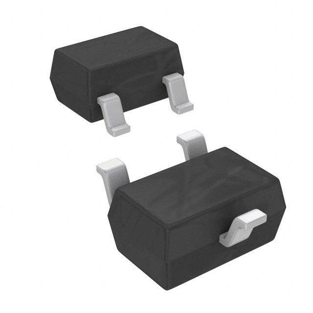
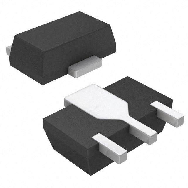
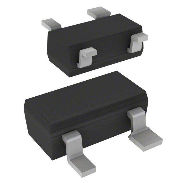
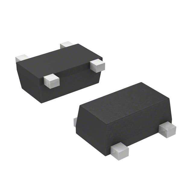
| 产品图片 |
|
| rohs | 符合RoHS无铅 / 符合限制有害物质指令(RoHS)规范要求 |
| 产品系列 | 晶体管,晶体管射频,射频双极晶体管,NXP Semiconductors BFT25A,215- |
| 数据手册 | |
| 产品型号 | BFT25A,215 |
| PCN封装 | |
| PCN设计/规格 | |
| 不同 Ic、Vce 时的DC电流增益(hFE)(最小值) | 50 @ 500µA, 1V |
| 产品目录页面 | |
| 产品种类 | 射频双极晶体管 |
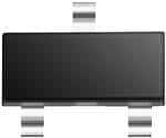
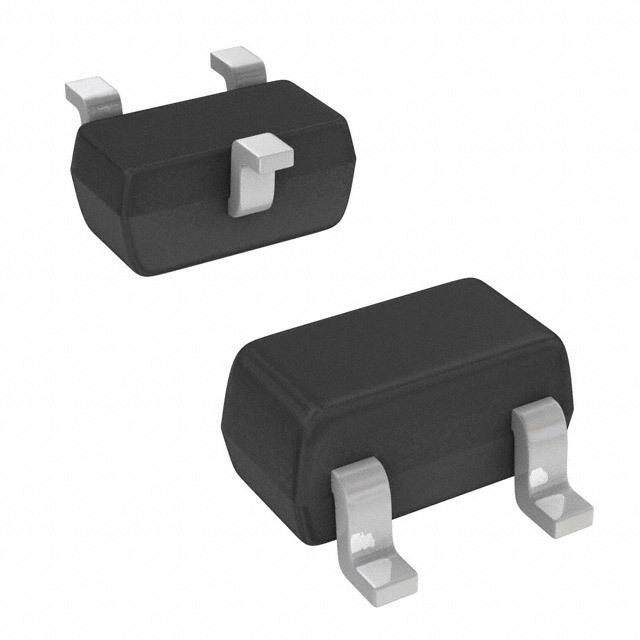
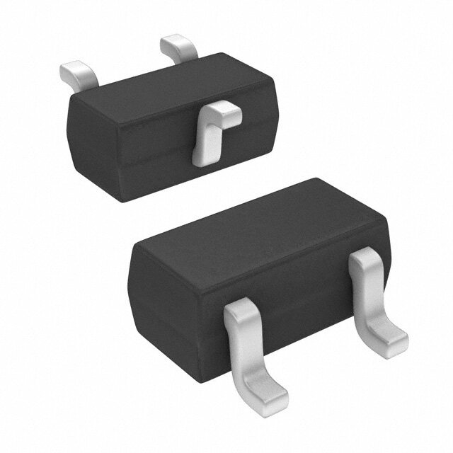
| 供应商器件封装 | SOT-23 (TO-236AB) |
| 其它名称 | 568-1992-2 |
| 功率-最大值 | 32mW |
| 功率耗散 | 32 mW |
| 包装 | 带卷 (TR) |
| 发射极-基极电压VEBO | 2 V |
| 商标 | NXP Semiconductors |
| 噪声系数(dB,不同f时的典型值) | 1.8dB ~ 2dB @ 1GHz |
| 增益 | - |
| 安装类型 | 表面贴装 |
| 安装风格 | SMD/SMT |
| 封装 | Reel |
| 封装/外壳 | TO-236-3,SC-59,SOT-23-3 |
| 封装/箱体 | SOT-23 |
| 工厂包装数量 | 3000 |
| 技术 | Silicon |
| 晶体管极性 | NPN |
| 晶体管类型 | Bipolar |
| 最大工作温度 | + 150 C |
| 最大工作频率 | 5000 MHz |
| 最大直流电集电极电流 | 0.0065 A |
| 最小工作温度 | - 65 C |
| 标准包装 | 3,000 |
| 电压-集射极击穿(最大值) | 5V |
| 电流-集电极(Ic)(最大值) | 6.5mA |
| 直流集电极/BaseGainhfeMin | 50 |
| 类型 | RF Bipolar Small Signal |
| 配置 | Single |
| 集电极—发射极最大电压VCEO | 5 V |
| 集电极连续电流 | 6.5 mA |
| 零件号别名 | BFT25A T/R |
| 频率 | 5000 MHz |
| 频率-跃迁 | 5GHz |


- 商务部:美国ITC正式对集成电路等产品启动337调查
- 曝三星4nm工艺存在良率问题 高通将骁龙8 Gen1或转产台积电
- 太阳诱电将投资9.5亿元在常州建新厂生产MLCC 预计2023年完工
- 英特尔发布欧洲新工厂建设计划 深化IDM 2.0 战略
- 台积电先进制程称霸业界 有大客户加持明年业绩稳了
- 达到5530亿美元!SIA预计今年全球半导体销售额将创下新高
- 英特尔拟将自动驾驶子公司Mobileye上市 估值或超500亿美元
- 三星加码芯片和SET,合并消费电子和移动部门,撤换高东真等 CEO
- 三星电子宣布重大人事变动 还合并消费电子和移动部门
- 海关总署:前11个月进口集成电路产品价值2.52万亿元 增长14.8%


PDF Datasheet 数据手册内容提取
BFT25A SOT23 NPN 5 GHz wideband transistor Rev. 5 — 12 September 2011 Product data sheet 1. Product profile 1.1 General description The BFT25A is a silicon NPN transistor, primarily intended for use in RF low power amplifiers, such as pocket telephones and paging systems with signal frequencies up to2GHz. The transistor is encapsulated in a 3-pin plastic SOT23 envelope. 1.2 Features and benefits Low current consumption (100 A to 1 mA) Low noise figure Gold metallization ensures excellent reliability. 1.3 Quick reference data Table 1. Quick reference data Symbol Parameter Conditions Min Typ Max Unit V collector-base open emitter - - 8 V CBO voltage V collector-emitter open base - - 5 V CEO voltage I DC collector - - 6.5 mA C current P total power up to T = 165 C [1] - - 32 mW tot s dissipation h DC current gain I = 0.5mA; V = 1V 50 80 200 FE C CE f transition I = 1mA; V = 1V; 3.5 5 - GHz T C CE frequency T =25C; amb f=500MHz G maximum I =0.5 mA; V = 1 V; - 15 - dB UM C CE unilateral power T = 25 C; amb gain f=1 GHz F noise figure = ; I =0.5 mA; - 1.8 - dB opt C V = 1 V; CE T =25 C; f = 1 GHz amb = ; I =1 mA; - 2 - dB opt C V = 1 V; CE T =25 C; f = 1 GHz amb [1] T is the temperature at the soldering point of the collector tab. s
BFT25A NXP Semiconductors NPN 5 GHz wideband transistor 2. Pinning information Table 2. Discrete pinning Pin Description Simplified outline Symbol Code: V10 3 3 1 base 2 emitter 1 3 collector 1 2 2 sym021 3. Ordering information Table 3. Ordering information Type number Package Name Description Version BFT25A - plastic surface mounted package; 3leads SOT23 4. Marking Table 4. Marking Type number Marking code[1] BFT25A 34* [1] * = p : Made in Hong Kong. * = t : Made in Malaysia. * = W : Made in China. 5. Limiting values Table 5. Limiting values In accordance with the Absolute Maximum Rating System (IEC 60134). Symbol Parameter Conditions Min Max Unit V collector-base voltage open emitter - 8 V CBO V collector-emitter voltage open base - 5 V CEO V emitter-base voltage open collector - 2 V EBO I DC collector current - 6.5 mA C P total power dissipation up to T =165C [1] - 32 mW tot s T storage temperature 65 +150 C stg T junction temperature - 175 C j [1] T is the temperature at the soldering point of the collector tab. s BFT25A All information provided in this document is subject to legal disclaimers. © NXP B.V. 2011. All rights reserved. Product data sheet Rev. 5 — 12 September 2011 2 of 15
BFT25A NXP Semiconductors NPN 5 GHz wideband transistor 6. Thermal characteristics Table 6. Thermal characteristics Symbol Parameter Conditions Typ Unit R from junction to soldering point [1] 260 K/W th(j-s) [1] T is the temperature at the soldering point of the collector tab. s 7. Characteristics Table 7. Characteristics T = 25 Cunless otherwise specified. j Symbol Parameter Conditions Min Typ Max Unit I collector cut-off I = 0A; V = 5V - - 50 nA CBO E CB current h DC current gain I = 0.5 mA; V = 1 V 50 80 200 FE C CE f transition I = 1 mA; V = 1 V; 3.5 5 - GHz T C CE frequency T = 25 C; amb f=500MHz C feedback I =i =0A; V =1 V; - 0.3 0.45 pF re C c CB capacitance f= 1 MHz G maximum I = 0.5mA; V = 1V; [1] - 15 - dB UM C CE unilateral power T = 25 C;f = 1GHz amb gain F noise figure = ; I =0.5 mA; - 1.8 - dB opt C V = 1 V; CE T =25C; f = 1 GHz amb = ; I =1 mA; - 2 - dB opt C V = 1 V; CE T =25C; f = 1 GHz amb [1] G is the maximum unilateral power gain, assuming S is zero and UM 12 2 S G = 10 log--------------------------2--1--------------------------dB UM 2 2 1– S 1– S 11 22 BFT25A All information provided in this document is subject to legal disclaimers. © NXP B.V. 2011. All rights reserved. Product data sheet Rev. 5 — 12 September 2011 3 of 15
BFT25A NXP Semiconductors NPN 5 GHz wideband transistor mbg247 mcd138 40 100 Ptot hFE (mW) 80 30 60 20 40 10 20 00 50 100 150 200 010−3 10−2 10−1 1 10 Ts (°C) IC (mA) V =1 V. CE Fig 1. Power derating curve. Fig 2. DC current gain as a function of collector current. mcd103 mcd140 0.4 6 Cre (pF) fT (GHz) 0.3 4 0.2 2 0.1 0 0 0 1 2 3 4 5 0 1 2 3 4 VCB (V) IC (mA) IC = ic=0A; f = 1 MHz. VCE=1 V; Tamb=25C; f= 500 MHz. Fig 3. Feedback capacitance as a function of Fig 4. Transition frequency as a function of collector collector-base voltage. current. Figure5, 6, 7 and 8, G =maximum unilateral power gain; MSG = maximum stable gain. UM BFT25A All information provided in this document is subject to legal disclaimers. © NXP B.V. 2011. All rights reserved. Product data sheet Rev. 5 — 12 September 2011 4 of 15
BFT25A NXP Semiconductors NPN 5 GHz wideband transistor mcd104 mcd105 25 20 gain GUM gain (dB) (dB) 20 GUM 15 15 MSG 10 10 MSG 5 5 0 0 0 0.5 1.0 1.5 2.0 0 0.5 1.0 1.5 2.0 IC (mA) IC (mA) V =1 V; f = 500 MHz. V =1 V; f = 1 GHz. CE CE Fig 5. Gain as a function of collector current. Fig 6. Gain as a function of collector current. mcd106 mcd107 50 50 gain gain (dB) (dB) 40 GUM 40 GUM 30 30 MSG 20 MSG 20 10 10 Gmax Gmax 0 0 10 102 103 104 10 102 103 104 f (MHz) f (MHz) V =1 V; I = 0.5 mA. V =1 V; I = 1 mA. CE C CE C Fig 7. Gain as a function of frequency. Fig 8. Gain as a function of frequency. BFT25A All information provided in this document is subject to legal disclaimers. © NXP B.V. 2011. All rights reserved. Product data sheet Rev. 5 — 12 September 2011 5 of 15
BFT25A NXP Semiconductors NPN 5 GHz wideband transistor mcd145 mcd146 4 4 F F (dB) f = (dB) IC = 2 GHz 2 mA 3 3 1 GHz 500 MHz 1 mA 2 2 0.5 mA 1 1 0 0 10−1 1 10 102 103 104 IC (mA) f (MHz) V =1 V. V =1 V. CE CE Fig 9. Minimum noise figure as a function of Fig 10. Minimum noise figure as a function of collector current. frequency. 1 0.5 2 pot. unst. region 6 dB 0.2 4 dB 5 stability circle 2.5 dB 10 +j 0.2 0.5 1 2 5 10 ∞ 0 Γ opt −j MSG Fmin = 1.9 dB 10 14.5 dB 0.2 13 dB 5 11 dB 0.5 2 1 mcd108 See Table8; Zo=50 . Average gain parameter: MSG = 14.5 dB. Fig 11. Noise circle figure. BFT25A All information provided in this document is subject to legal disclaimers. © NXP B.V. 2011. All rights reserved. Product data sheet Rev. 5 — 12 September 2011 6 of 15
BFT25A NXP Semiconductors NPN 5 GHz wideband transistor Table 8. Noise parameters f (MHz) V (V) I (mA) F (dB) R /50 CE C min opt n (mag) (ang) 500 1 1 1.9 0.79 4 2.5 1 0.5 2 pot. unst. region 8 dB stability circle 0.2 4 dB 5 3 dB 10 +j 0.2 0.5 1 2 5 10 ∞ 0 MSG Γ −j 11.2 dB Fmionp =t 2 dB 10 10 dB 0.2 5 8 dB 0.5 2 1 mcd109 See Table9; Zo=50 . Average gain parameter: MSG = 11.2 dB. Fig 12. Noise circle figure. T able 9. Noise parameters f (MHz) V (V) I (mA) F (dB) R /50 CE C min opt n (mag) (ang) 1000 1 1 2 0.74 8 2.6 BFT25A All information provided in this document is subject to legal disclaimers. © NXP B.V. 2011. All rights reserved. Product data sheet Rev. 5 — 12 September 2011 7 of 15
BFT25A NXP Semiconductors NPN 5 GHz wideband transistor pot. unst. 1 stability region circle 0.5 2 MSG 7.7 dB 0.2 7 dB Γopt 5 Fmin = 2.4 dB 10 +j 3 dB 0.2 0.5 1 2 5 10 ∞ 0 −j 5 dB 4 dB 10 6 dB 0.2 5 0.5 2 1 mcd110 See Table10; Zo=50 . Average gain parameter: MSG = 7.7 dB. Fig 13. Noise circle figure. T able 10. Noise parameters f (MHz) V (V) I (mA) F (dB) R /50 CE C min opt n (mag) (ang) 2000 1 1 2.4 0.72 26 1.7 BFT25A All information provided in this document is subject to legal disclaimers. © NXP B.V. 2011. All rights reserved. Product data sheet Rev. 5 — 12 September 2011 8 of 15
BFT25A NXP Semiconductors NPN 5 GHz wideband transistor 1 0.5 2 0.2 5 10 +j 0.2 0.5 1 2 5 10 ∞ 0 40 MHz −j 3 GHz 10 0.2 5 0.5 2 1 mcd111 V =1 V; I =1 mA. CE C Zo = 50 . Fig 14. Common emitter input reflection coefficient (S ). 11 90° 135° 45° 3 GHz 40 MHz 180° 0° 5 4 3 2 1 0 −135° −45° −90° mcd112 V =1 V; I =1 mA. CE C Fig 15. Common emitter forward transmission coefficient (S ). 21 BFT25A All information provided in this document is subject to legal disclaimers. © NXP B.V. 2011. All rights reserved. Product data sheet Rev. 5 — 12 September 2011 9 of 15
BFT25A NXP Semiconductors NPN 5 GHz wideband transistor 90° 135° 45° 3 GHz 40 MHz 180° 0° 0.5 0.4 0.3 0.2 0.1 0 −135° −45° −90° mcd114 V =1 V; I =1 mA. CE C Fig 16. Common emitter reverse transmission coefficient (S ). 12 1 0.5 2 0.2 5 10 +j 0.2 0.5 1 2 5 10 ∞ 0 −j 40 MHz 10 0.2 3 GHz 5 0.5 2 1 mcd113 V =1 V; I =1 mA. CE C Zo = 50 . Fig 17. Common emitter output reflection coefficient (S ). 22 BFT25A All information provided in this document is subject to legal disclaimers. © NXP B.V. 2011. All rights reserved. Product data sheet Rev. 5 — 12 September 2011 10 of 15
BFT25A NXP Semiconductors NPN 5 GHz wideband transistor 8. Package outline Plastic surface-mounted package; 3 leads SOT23 D B E A X HE v M A 3 Q A A1 1 2 c e1 bp w M B Lp e detail X 0 1 2 mm scale DIMENSIONS (mm are the original dimensions) UNIT A mAa1x. bp c D E e e1 HE Lp Q v w 1.1 0.48 0.15 3.0 1.4 2.5 0.45 0.55 mm 0.1 1.9 0.95 0.2 0.1 0.9 0.38 0.09 2.8 1.2 2.1 0.15 0.45 OUTLINE REFERENCES EUROPEAN ISSUE DATE VERSION IEC JEDEC JEITA PROJECTION 04-11-04 SOT23 TO-236AB 06-03-16 Fig 18. Package outline. BFT25A All information provided in this document is subject to legal disclaimers. © NXP B.V. 2011. All rights reserved. Product data sheet Rev. 5 — 12 September 2011 11 of 15
BFT25A NXP Semiconductors NPN 5 GHz wideband transistor 9. Revision history Table 11. Revision history Document ID Release date Data sheet status Change notice Supersedes BFT25A v.5 20110912 Product data sheet - BFT25A v.4 Modifications: • The format of this data sheet has been redesigned to comply with the new identity guidelines of NXP Semiconductors. • Legal texts have been adapted to the new company name where appropriate. • Package outline drawings have been updated to the latest version. BFT25A v.4 20040706 Product data sheet - BFT25A_CNV v.3 (9397 750 13399) BFT25A_CNV v.3 19971205 Product specification - - BFT25A All information provided in this document is subject to legal disclaimers. © NXP B.V. 2011. All rights reserved. Product data sheet Rev. 5 — 12 September 2011 12 of 15
BFT25A NXP Semiconductors NPN 5 GHz wideband transistor 10. Legal information 10.1 Data sheet status Document status[1][2] Product status[3] Definition Objective [short] data sheet Development This document contains data from the objective specification for product development. Preliminary [short] data sheet Qualification This document contains data from the preliminary specification. Product [short] data sheet Production This document contains the product specification. [1] Please consult the most recently issued document before initiating or completing a design. [2] The term ‘short data sheet’ is explained in section “Definitions”. [3] The product status of device(s) described in this document may have changed since this document was published and may differ in case of multiple devices. The latest product status information is available on the Internet at URLhttp://www.nxp.com. 10.2 Definitions malfunction of an NXP Semiconductors product can reasonably be expected to result in personal injury, death or severe property or environmental damage. NXP Semiconductors accepts no liability for inclusion and/or use of Draft — The document is a draft version only. The content is still under NXP Semiconductors products in such equipment or applications and internal review and subject to formal approval, which may result in therefore such inclusion and/or use is at the customer’s own risk. modifications or additions. NXP Semiconductors does not give any representations or warranties as to the accuracy or completeness of Applications — Applications that are described herein for any of these information included herein and shall have no liability for the consequences of products are for illustrative purposes only. NXP Semiconductors makes no use of such information. representation or warranty that such applications will be suitable for the specified use without further testing or modification. Short data sheet — A short data sheet is an extract from a full data sheet with the same product type number(s) and title. A short data sheet is intended Customers are responsible for the design and operation of their applications for quick reference only and should not be relied upon to contain detailed and and products using NXP Semiconductors products, and NXP Semiconductors full information. For detailed and full information see the relevant full data accepts no liability for any assistance with applications or customer product sheet, which is available on request via the local NXP Semiconductors sales design. It is customer’s sole responsibility to determine whether the NXP office. In case of any inconsistency or conflict with the short data sheet, the Semiconductors product is suitable and fit for the customer’s applications and full data sheet shall prevail. products planned, as well as for the planned application and use of customer’s third party customer(s). Customers should provide appropriate Product specification — The information and data provided in a Product design and operating safeguards to minimize the risks associated with their data sheet shall define the specification of the product as agreed between applications and products. NXP Semiconductors and its customer, unless NXP Semiconductors and NXP Semiconductors does not accept any liability related to any default, customer have explicitly agreed otherwise in writing. In no event however, damage, costs or problem which is based on any weakness or default in the shall an agreement be valid in which the NXP Semiconductors product is customer’s applications or products, or the application or use by customer’s deemed to offer functions and qualities beyond those described in the third party customer(s). Customer is responsible for doing all necessary Product data sheet. testing for the customer’s applications and products using NXP Semiconductors products in order to avoid a default of the applications and 10.3 Disclaimers the products or of the application or use by customer’s third party customer(s). NXP does not accept any liability in this respect. Limited warranty and liability — Information in this document is believed to Limiting values — Stress above one or more limiting values (as defined in be accurate and reliable. However, NXP Semiconductors does not give any the Absolute Maximum Ratings System of IEC60134) will cause permanent representations or warranties, expressed or implied, as to the accuracy or damage to the device. Limiting values are stress ratings only and (proper) completeness of such information and shall have no liability for the operation of the device at these or any other conditions above those given in consequences of use of such information. the Recommended operating conditions section (if present) or the Characteristics sections of this document is not warranted. Constant or In no event shall NXP Semiconductors be liable for any indirect, incidental, repeated exposure to limiting values will permanently and irreversibly affect punitive, special or consequential damages (including - without limitation - lost the quality and reliability of the device. profits, lost savings, business interruption, costs related to the removal or replacement of any products or rework charges) whether or not such Terms and conditions of commercial sale — NXP Semiconductors damages are based on tort (including negligence), warranty, breach of products are sold subject to the general terms and conditions of commercial contract or any other legal theory. sale, as published at http://www.nxp.com/profile/terms, unless otherwise Notwithstanding any damages that customer might incur for any reason agreed in a valid written individual agreement. In case an individual whatsoever, NXP Semiconductors’ aggregate and cumulative liability towards agreement is concluded only the terms and conditions of the respective customer for the products described herein shall be limited in accordance agreement shall apply. NXP Semiconductors hereby expressly objects to with the Terms and conditions of commercial sale of NXP Semiconductors. applying the customer’s general terms and conditions with regard to the purchase of NXP Semiconductors products by customer. Right to make changes — NXP Semiconductors reserves the right to make changes to information published in this document, including without No offer to sell or license — Nothing in this document may be interpreted or limitation specifications and product descriptions, at any time and without construed as an offer to sell products that is open for acceptance or the grant, notice. This document supersedes and replaces all information supplied prior conveyance or implication of any license under any copyrights, patents or to the publication hereof. other industrial or intellectual property rights. Suitability for use — NXP Semiconductors products are not designed, Export control — This document as well as the item(s) described herein authorized or warranted to be suitable for use in life support, life-critical or may be subject to export control regulations. Export might require a prior safety-critical systems or equipment, nor in applications where failure or authorization from national authorities. BFT25A All information provided in this document is subject to legal disclaimers. © NXP B.V. 2011. All rights reserved. Product data sheet Rev. 5 — 12 September 2011 13 of 15
BFT25A NXP Semiconductors NPN 5 GHz wideband transistor Quick reference data — The Quick reference data is an extract of the product for such automotive applications, use and specifications, and (b) product data given in the Limiting values and Characteristics sections of this whenever customer uses the product for automotive applications beyond document, and as such is not complete, exhaustive or legally binding. NXP Semiconductors’ specifications such use shall be solely at customer’s own risk, and (c) customer fully indemnifies NXP Semiconductors for any Non-automotive qualified products — Unless this data sheet expressly liability, damages or failed product claims resulting from customer design and states that this specific NXP Semiconductors product is automotive qualified, use of the product for automotive applications beyond NXP Semiconductors’ the product is not suitable for automotive use. It is neither qualified nor tested standard warranty and NXP Semiconductors’ product specifications. in accordance with automotive testing or application requirements. NXP Semiconductors accepts no liability for inclusion and/or use of non-automotive qualified products in automotive equipment or applications. 10.4 Trademarks In the event that customer uses the product for design-in and use in automotive applications to automotive specifications and standards, customer Notice: All referenced brands, product names, service names and trademarks (a) shall use the product without NXP Semiconductors’ warranty of the are the property of their respective owners. 11. Contact information For more information, please visit: http://www.nxp.com For sales office addresses, please send an email to: salesaddresses@nxp.com BFT25A All information provided in this document is subject to legal disclaimers. © NXP B.V. 2011. All rights reserved. Product data sheet Rev. 5 — 12 September 2011 14 of 15
BFT25A NXP Semiconductors NPN 5 GHz wideband transistor 12. Contents 1 Product profile. . . . . . . . . . . . . . . . . . . . . . . . . . 1 1.1 General description . . . . . . . . . . . . . . . . . . . . . 1 1.2 Features and benefits. . . . . . . . . . . . . . . . . . . . 1 1.3 Quick reference data . . . . . . . . . . . . . . . . . . . . 1 2 Pinning information. . . . . . . . . . . . . . . . . . . . . . 2 3 Ordering information. . . . . . . . . . . . . . . . . . . . . 2 4 Marking. . . . . . . . . . . . . . . . . . . . . . . . . . . . . . . . 2 5 Limiting values. . . . . . . . . . . . . . . . . . . . . . . . . . 2 6 Thermal characteristics . . . . . . . . . . . . . . . . . . 3 7 Characteristics. . . . . . . . . . . . . . . . . . . . . . . . . . 3 8 Package outline. . . . . . . . . . . . . . . . . . . . . . . . 11 9 Revision history. . . . . . . . . . . . . . . . . . . . . . . . 12 10 Legal information. . . . . . . . . . . . . . . . . . . . . . . 13 10.1 Data sheet status . . . . . . . . . . . . . . . . . . . . . . 13 10.2 Definitions. . . . . . . . . . . . . . . . . . . . . . . . . . . . 13 10.3 Disclaimers. . . . . . . . . . . . . . . . . . . . . . . . . . . 13 10.4 Trademarks. . . . . . . . . . . . . . . . . . . . . . . . . . . 14 11 Contact information. . . . . . . . . . . . . . . . . . . . . 14 12 Contents. . . . . . . . . . . . . . . . . . . . . . . . . . . . . . 15 Please be aware that important notices concerning this document and the product(s) described herein, have been included in section ‘Legal information’. © NXP B.V. 2011. All rights reserved. For more information, please visit: http://www.nxp.com For sales office addresses, please send an email to: salesaddresses@nxp.com Date of release: 12 September 2011 Document identifier: BFT25A
Mouser Electronics Authorized Distributor Click to View Pricing, Inventory, Delivery & Lifecycle Information: N XP: BFT25A,215