ICGOO在线商城 > 分立半导体产品 > 晶体管 - UGBT,MOSFET - 单 > STGB18N40LZT4
 Datasheet下载
- 型号: STGB18N40LZT4
- 制造商: STMicroelectronics
- 库位|库存: xxxx|xxxx
- 要求:
| 数量阶梯 | 香港交货 | 国内含税 |
| +xxxx | $xxxx | ¥xxxx |
查看当月历史价格
查看今年历史价格
STGB18N40LZT4产品简介:
ICGOO电子元器件商城为您提供STGB18N40LZT4由STMicroelectronics设计生产,在icgoo商城现货销售,并且可以通过原厂、代理商等渠道进行代购。 STGB18N40LZT4价格参考。STMicroelectronicsSTGB18N40LZT4封装/规格:晶体管 - UGBT,MOSFET - 单, IGBT 420V 30A 150W Surface Mount D2PAK。您可以下载STGB18N40LZT4参考资料、Datasheet数据手册功能说明书,资料中有STGB18N40LZT4 详细功能的应用电路图电压和使用方法及教程。
STMicroelectronics的STGB18N40LZT4是一款功率MOSFET器件,属于晶体管中的IGBT/MOSFET类别。该器件常用于需要高效能功率转换与控制的场景,其应用场景主要包括:

1. 电源管理:适用于开关电源(SMPS)、DC-DC转换器和AC-DC电源适配器,提供高效能和低导通损耗。

2. 电机驱动:可用于工业自动化设备、电动工具和家用电器中的电机控制,具备高耐压和大电流承载能力。

3. 照明系统:如LED照明驱动电路,支持高效能和稳定输出。

4. 消费类电子产品:如电视、音响设备中的电源部分,提供紧凑、高效的功率解决方案。

5. 新能源应用:如太阳能逆变器、储能系统中的功率转换模块。

该器件采用表面贴装封装,适合自动化生产,广泛应用于对效率、可靠性要求较高的中高功率电子系统中。
| 参数 | 数值 |
| 25°C时Td(开/关)值 | 650ns/13.5µs |
| 产品目录 | |
| Current-CollectorPulsed(Icm) | 40A |
| 描述 | IGBT 420V 30A 150W D2PAKIGBT 晶体管 EAS 180 mJ-400 V |
| 产品分类 | IGBT - 单路分离式半导体 |
| GateCharge | 29nc |
| IGBT类型 | - |
| 品牌 | STMicroelectronics |
| 产品手册 | |
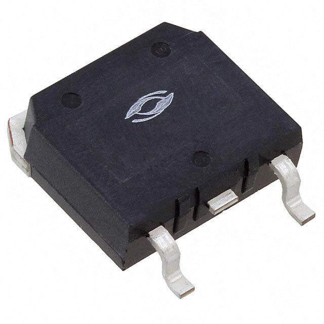
| 产品图片 |
|
| rohs | 符合RoHS无铅 / 符合限制有害物质指令(RoHS)规范要求 |
| 产品系列 | 晶体管,IGBT 晶体管,STMicroelectronics STGB18N40LZT4PowerMESH™ |
| 数据手册 | |
| 产品型号 | STGB18N40LZT4 |
| SwitchingEnergy | - |
| TestCondition | 300V, 10A, 5V |
| 不同 Vge、Ic时的 Vce(on) | 1.7V @ 4.5V,10A |
| 产品目录页面 | |
| 产品种类 | IGBT 晶体管 |
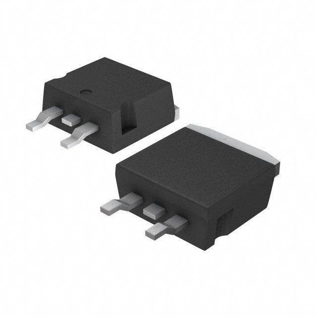
| 供应商器件封装 | D2PAK |
| 其它名称 | 497-7006-1 |
| 其它有关文件 | http://www.st.com/web/catalog/sense_power/FM100/CL826/SC1131/PF184846?referrer=70071840 |
| 功率-最大值 | 150W |
| 包装 | 剪切带 (CT) |
| 反向恢复时间(trr) | - |
| 商标 | STMicroelectronics |
| 安装类型 | 表面贴装 |
| 安装风格 | SMD/SMT |
| 封装 | Reel |
| 封装/外壳 | TO-263-3,D²Pak(2 引线+接片),TO-263AB |
| 封装/箱体 | D2PAK-3 |
| 工厂包装数量 | 1000 |
| 最大工作温度 | + 150 C |
| 最小工作温度 | - 55 C |
| 栅极/发射极最大电压 | 12 V |
| 标准包装 | 1 |
| 特色产品 | http://www.digikey.cn/product-highlights/zh/tailless-600-v-igbt-v-series/51749 |
| 电压-集射极击穿(最大值) | 420V |
| 电流-集电极(Ic)(最大值) | 30A |
| 系列 | STGB18N40LZ |
| 输入类型 | 逻辑 |
| 配置 | Single |
| 集电极—发射极最大电压VCEO | 360 V |
| 集电极最大连续电流Ic | 30 A |


- 商务部:美国ITC正式对集成电路等产品启动337调查
- 曝三星4nm工艺存在良率问题 高通将骁龙8 Gen1或转产台积电
- 太阳诱电将投资9.5亿元在常州建新厂生产MLCC 预计2023年完工
- 英特尔发布欧洲新工厂建设计划 深化IDM 2.0 战略
- 台积电先进制程称霸业界 有大客户加持明年业绩稳了
- 达到5530亿美元!SIA预计今年全球半导体销售额将创下新高
- 英特尔拟将自动驾驶子公司Mobileye上市 估值或超500亿美元
- 三星加码芯片和SET,合并消费电子和移动部门,撤换高东真等 CEO
- 三星电子宣布重大人事变动 还合并消费电子和移动部门
- 海关总署:前11个月进口集成电路产品价值2.52万亿元 增长14.8%


PDF Datasheet 数据手册内容提取
STGB18N40LZT4, STGD18N40LZ, STGP18N40LZ Automotive-grade 390 V internally clamped IGBT E 180 mJ SCIS Datasheet - production data Features (cid:55)(cid:36)(cid:37) (cid:55)(cid:36)(cid:37) • Designed for automotive applications and (cid:22) AEC-Q101 qualified (cid:22) (cid:20) (cid:20)(cid:21) (cid:39)(cid:51)(cid:36)(cid:46) • 180 mJ of avalanche energy @ TC = 150 °C, L = 3 mH (cid:44)(cid:51)(cid:36)(cid:46) • ESD gate-emitter protection (cid:55)(cid:36)(cid:37) • Gate-collector high voltage clamping (cid:55)(cid:36)(cid:37) • Logic level gate drive • Low saturation voltage (cid:22) (cid:21) (cid:22) (cid:20) (cid:20) • High pulsed current capability (cid:55)(cid:50)(cid:16)(cid:21)(cid:21)(cid:19) (cid:39)(cid:240)(cid:51)(cid:36)(cid:46) • Gate and gate-emitter resistor Application Figure 1. Internal schematic diagram C (2 or TAB) • Pencil coil electronic ignition driver Description This application-specific IGBT utilizes the most advanced PowerMESH™ technology. The built-in RG Zener diodes between gate-collector and gate- G (1) emitter provide overvoltage protection capabilities. The device also exhibits low on-state RGE voltage drop and low threshold drive for use in automotive ignition system. E (3) SC30180 Table 1. Device summary Order codes Marking Package Packaging STGB18N40LZT4 GB18N40LZ D²PAK Tape and reel STGD18N40LZ-1 GD18N40LZ IPAK Tube STGD18N40LZT4 GD18N40LZ DPAK Tape and reel STGP18N40LZ GP18N40LZ TO-220 Tube November 2014 DocID14322 Rev 6 1/25 This is information on a product in full production. www.st.com
Contents STGB18N40LZT4 , STGD18N40LZ ,STGP18N40LZT4 Contents 1 Electrical ratings . . . . . . . . . . . . . . . . . . . . . . . . . . . . . . . . . . . . . . . . . . . . 3 2 Electrical characteristics . . . . . . . . . . . . . . . . . . . . . . . . . . . . . . . . . . . . . 4 2.1 Electrical characteristics (curves) . . . . . . . . . . . . . . . . . . . . . . . . . . . . 6 3 Test circuits . . . . . . . . . . . . . . . . . . . . . . . . . . . . . . . . . . . . . . . . . . . . . . . 9 4 Package mechanical data . . . . . . . . . . . . . . . . . . . . . . . . . . . . . . . . . . . . 10 4.1 STGB18N40LZT4, D2PAK . . . . . . . . . . . . . . . . . . . . . . . . . . . . . . . . . . . . .11 4.2 STGD18N40LZ-1, IPAK . . . . . . . . . . . . . . . . . . . . . . . . . . . . . . . . . . . . . . 14 4.3 STGD18N40LZT4, DPAK . . . . . . . . . . . . . . . . . . . . . . . . . . . . . . . . . . . . . 16 4.4 STGP18N40LZ, TO-220 . . . . . . . . . . . . . . . . . . . . . . . . . . . . . . . . . . . . . . 19 5 Packaging mechanical data . . . . . . . . . . . . . . . . . . . . . . . . . . . . . . . . . . 21 6 Revision history . . . . . . . . . . . . . . . . . . . . . . . . . . . . . . . . . . . . . . . . . . . 24 2/25 DocID14322 Rev 6
STGB18N40LZT4 , STGD18N40LZ ,STGP18N40LZT4 Electrical ratings 1 Electrical ratings Table 2. Absolute maximum ratings Symbol Parameter Value Unit V Collector-emitter voltage (v = 0) V V CES GE CES(clamped) V Emitter collector voltage (V = 0) 20 V ECS GE I (1) Collector current (continuous) at T = 100 °C 30 A C C I (2) Pulsed collector current 40 A CP V Gate-emitter voltage V V GE GE(clamped) P Total dissipation at T = 25 °C 150 W TOT C Single pulse energy T = 25 °C, L = 3 mH, V = 50 V 300 mJ E (3) C CC SCIS Single pulse energy T =150 °C, L = 3 mH, V = 50 V 180 mJ C CC Human body model, R= 1.5 kΩ, C = 100 pF 8 kV ESD Machine model, R = 0, C = 100 pF 800 V Charged device model 2 kV T Storage temperature stg – 55 to 175 °C T Operating junction temperature j 1. Calculated according to the iterative formula T –T I (T ) = ----------------------------------------j--(--m----a---x---)-----------C-------------------------------------- C C R ×V (T ,I (T )) thj–c CE(sat)(max) j(max) C C 2. Pulse width limited by max. junction temperature 3. For E test circuit refer to Figure 16.: Inductive load switching and E test circuit with A and B not SCIS SCIS connected. Table 3. Thermal data Value Symbol Parameter Unit DPAK D²PAK IPAK TO-220 R Thermal resistance junction-case 1 °C/W thj-case R Thermal resistance junction-ambient 100 62.5 °C/W thj-amb DocID14322 Rev 6 3/25 25
Electrical characteristics STGB18N40LZT4 , STGD18N40LZ ,STGP18N40LZT4 2 Electrical characteristics (T =25 °C unless otherwise specified) J Table 4. Static electrical characteristics Symbol Parameter Test conditions Min. Typ. Max. Unit Collector emitter I = 2 mA V clamped voltage C 360 390 420 V CES(clamped) T = - 40 °C to 150 °C (V = 0) J GE Emitter collector V break-down voltage I = 75 mA 20 28 V (BR)ECS C (V = 0) GE Gate emitter V I = ±2 mA 12 16 V GE(clamped) clamped voltage G Collector cut-off V = 15 V, T = 150 °C 10 µA CE J I current CES V = 200 V, T = 150 °C 100 µA (V = 0) CE J GE Gate-emitter I leakage current V = ±10 V 450 625 830 µA GES GE (V = 0) CE Gate emitter R 12 16 22 kΩ GE resistance R Gate resistance 1.6 kΩ G V =V , I = 1 mA, T = -40 °C 1.4 V GE CE C J Gate threshold V V =V , I = 1 mA 1.2 1.6 2.3 V GE(th) voltage GE CE C V =V , I = 1 mA, T =150 °C 0.7 V GE CE C J V = 4.5 V, I = 10 A 1.35 1.7 V GE C V Collector emitter VGE = 4.5 V, IC = 10 A, 1.30 V CE(sat) saturation voltage T = 150 °C J V = 3.8 V, I = 6 A 1.30 V GE C Table 5. Dynamic electrical characteristics Symbol Parameter Test conditions Min. Typ. Max. Unit C Input capacitance - 490 - pF ies Coes Output capacitance VCE = 25 V, f = 1 MHz, - 90 - pF V = 0 Reverse transfer GE C - 5 - pF res capacitance V = 280 V, I = 10 A, Q Gate charge CE C - 29 - nC g V = 5 V GE 4/25 DocID14322 Rev 6
STGB18N40LZT4 , STGD18N40LZ ,STGP18N40LZT4 Electrical characteristics Table 6. Resistive load switching time Symbol Parameter Test conditions Min. Typ. Max. Unit td(on) Turn-on delay time VCC = 14 V, - 0.65 - µs tr Rise time RL = 1 Ω, VGE = 5 V - 3.5 - µs td(on) Turn-on delay time VCC= 14V, RL= 1Ω, - 0.65 - µs tr Rise time VGE= 5V, TJ= 150 °C - 3.8 - µs Table 7. Inductive load switching time Symbol Parameter Test conditions Min. Typ. Max. Unit t Turn-off delay time - 13.5 - µs d(off) V = 300 V, L = 1 mH t Fall time CC - 5.5 - µs f I = 10 A, V = 5 V C GE dv/dt Turn-off voltage slope - 105 - V/µs t Turn-off delay time - 14.2 - µs d(off) V = 300 V, L = 1 mH CC t Fall time I = 10 A, V = 5 V - 8 - µs f C GE T = 150 °C dv/dt Turn-off voltage slope J - 97 - V/µs DocID14322 Rev 6 5/25 25
Electrical characteristics STGB18N40LZT4 , STGD18N40LZ ,STGP18N40LZT4 2.1 Electrical characteristics (curves) Figure 2. Collector-emitter on voltage vs Figure 3. Collector-emitter on voltage vs temperature temperature Figure 4. Collector-emitter on voltage vs Figure 5. Self clamped inductive switch temperature ISCIS AM03942v1 (A) V =5V GE 24 VCE=50V 16 T=25°C J 8 T=150°C J 0 0 2 4 6 8 L(mH) 6/25 DocID14322 Rev 6
STGB18N40LZT4 , STGD18N40LZ ,STGP18N40LZT4 Electrical characteristics Figure 6. Output characteristics @ 25 °C Figure 7. Output characteristics @ -40 °C IC (6A0) HV42380 IC (6A0) HV42390 VGE = 8 V VGE = 4.5 V VGE = 8 V V = 4.5 V 50 50 GE → VGE = 5 V VGE = 4 V VGE = 5 V VGE = 4 V 40 40 30 VGE = 3.8 V 30 VGE = 3.8 V 20 20 TC = 25 °C TC = -40 °C 10 10 0 0 0 1 2 3 4 5 VCE (V) 0 1 2 3 4 5 VCE (V)6 Figure 8. Output characteristics @ 175 °C Figure 9. Transfer characteristics IC (6A0) HV42400 IICC ((44AA00)) HV38710 VGE = 8 V VGE = 5 V 3355 50 V = 4.5 V GE 3300 VVCCEE== 55VV 40 V = 4 V 2255 GE 2200 30 V = 3.8 V GE 1155 117755°°CC 20 1100 T = 175 °C C 2255°°CC 10 55 --4400°°CC 00 0 0 1 2 3 4 5 VCE (V)6 11..00 11..55 22..00 22..55 33..00 33..55 44..00 44..55 VV55GG..EE00 ((VV)) Figure 10. Collector cut-off current vs. Figure 11. Normalized collector emitter voltage temperature vs temperature DocID14322 Rev 6 7/25 25
Electrical characteristics STGB18N40LZT4 , STGD18N40LZ ,STGP18N40LZT4 Figure 12. Normalized gate threshold voltage vs Figure 13. Normalized collector emitter on temperature voltage vs temperature Figure 14. Thermal impedance for D²PAK, Figure 15. Thermal impedance for DPAK, IPAK I²PAK, TO-220 8/25 DocID14322 Rev 6
STGB18N40LZT4 , STGD18N40LZ ,STGP18N40LZT4 Test circuits 3 Test circuits Figure 16. Inductive load switching and E Figure 17. Resistive load switching SCIS test circuit L AM01504v1 AM01504v2 Figure 18. Gate charge test circuit Figure 19. Switching waveform k 90% k VG 10% 90% VCE 10% Tr(Voff) k Tcross 90% k IC TdT(oonn) Tr(Ion) Td(oTofff)f Tf 10% k k AM01505v1 AM01506v1 DocID14322 Rev 6 9/25 25
Package mechanical data STGB18N40LZT4 , STGD18N40LZ ,STGP18N40LZT4 4 Package mechanical data In order to meet environmental requirements, ST offers these devices in different grades of ECOPACK® packages, depending on their level of environmental compliance. ECOPACK® specifications, grade definitions and product status are available at: www.st.com. ECOPACK is an ST trademark. 10/25 DocID14322 Rev 6
STGB18N40LZT4 , STGD18N40LZ ,STGP18N40LZT4 Package mechanical data 2 4.1 STGB18N40LZT4, D PAK Figure 20. D²PAK (TO-263) drawing (cid:19)(cid:19)(cid:26)(cid:28)(cid:23)(cid:24)(cid:26)(cid:66)(cid:56) DocID14322 Rev 6 11/25 25
Package mechanical data STGB18N40LZT4 , STGD18N40LZ ,STGP18N40LZT4 Table 8. D²PAK (TO-263) mechanical data mm Dim. Min. Typ. Max. A 4.40 4.60 A1 0.03 0.23 b 0.70 0.93 b2 1.14 1.70 c 0.45 0.60 c2 1.23 1.36 D 8.95 9.35 D1 7.50 7.75 8.00 D2 1.10 1.30 1.50 E 10 10.40 E1 8.50 8.70 8.90 E2 6.85 7.05 7.25 e 2.54 e1 4.88 5.28 H 15 15.85 J1 2.49 2.69 L 2.29 2.79 L1 1.27 1.40 L2 1.30 1.75 R 0.4 V2 0° 8° 12/25 DocID14322 Rev 6
STGB18N40LZT4 , STGD18N40LZ ,STGP18N40LZT4 Package mechanical data Figure 21. D²PAK footprint(a) Footprint a. All dimension are in millimeters DocID14322 Rev 6 13/25 25
Package mechanical data STGB18N40LZT4 , STGD18N40LZ ,STGP18N40LZT4 4.2 STGD18N40LZ-1, IPAK Figure 22. IPAK (TO-251) type A drawing 0068771_L 14/25 DocID14322 Rev 6
STGB18N40LZT4 , STGD18N40LZ ,STGP18N40LZT4 Package mechanical data Table 9. IPAK (TO-251) type A mechanical data mm. DIM min. typ. max. A 2.20 2.40 A1 0.90 1.10 b 0.64 0.90 b2 0.95 b4 5.20 5.40 B5 0.30 c 0.45 0.60 c2 0.48 0.60 D 6.00 6.20 E 6.40 6.60 e 2.28 e1 4.40 4.60 H 16.10 L 9.00 9.40 L1 0.80 1.20 L2 0.80 1.00 V1 10° DocID14322 Rev 6 15/25 25
Package mechanical data STGB18N40LZT4 , STGD18N40LZ ,STGP18N40LZT4 4.3 STGD18N40LZT4, DPAK Figure 23. DPAK (TO-252) type A drawing (cid:19)(cid:19)(cid:25)(cid:27)(cid:26)(cid:26)(cid:21)(cid:66)(cid:52) 16/25 DocID14322 Rev 6
STGB18N40LZT4 , STGD18N40LZ ,STGP18N40LZT4 Package mechanical data Table 10. DPAK (TO-252) type A mechanical data mm Dim. Min. Typ. Max. A 2.20 2.40 A1 0.90 1.10 A2 0.03 0.23 b 0.64 0.90 b4 5.20 5.40 c 0.45 0.60 c2 0.48 0.60 D 6.00 6.20 D1 5.10 E 6.40 6.60 E1 4.70 e 2.28 e1 4.40 4.60 H 9.35 10.10 L 1.00 1.50 L1 2.80 L2 0.80 L4 0.60 1.00 R 0.20 V2 0° 8° DocID14322 Rev 6 17/25 25
Package mechanical data STGB18N40LZT4 , STGD18N40LZ ,STGP18N40LZT4 Figure 24. DPAK (TO-252) footprint (b) (cid:41)(cid:51)(cid:19)(cid:19)(cid:25)(cid:27)(cid:26)(cid:26)(cid:21)(cid:66)(cid:52) b. All dimensions are in millimeters 18/25 DocID14322 Rev 6
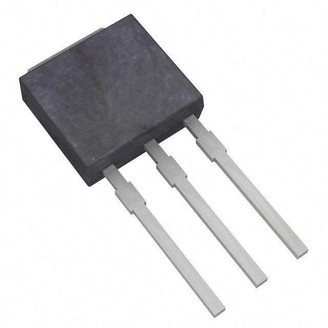
STGB18N40LZT4 , STGD18N40LZ ,STGP18N40LZT4 Package mechanical data 4.4 STGP18N40LZ, TO-220 Figure 25. TO-220 type A drawing (cid:19)(cid:19)(cid:20)(cid:24)(cid:28)(cid:27)(cid:27)(cid:66)(cid:87)(cid:92)(cid:83)(cid:72)(cid:36)(cid:66)(cid:53)(cid:72)(cid:89)(cid:66)(cid:55) DocID14322 Rev 6 19/25 25
Package mechanical data STGB18N40LZT4 , STGD18N40LZ ,STGP18N40LZT4 Table 11. TO-220 type A mechanical data mm Dim. Min. Typ. Max. A 4.40 4.60 b 0.61 0.88 b1 1.14 1.70 c 0.48 0.70 D 15.25 15.75 D1 1.27 E 10 10.40 e 2.40 2.70 e1 4.95 5.15 F 1.23 1.32 H1 6.20 6.60 J1 2.40 2.72 L 13 14 L1 3.50 3.93 L20 16.40 L30 28.90 øP 3.75 3.85 Q 2.65 2.95 20/25 DocID14322 Rev 6
STGB18N40LZT4 , STGD18N40LZ ,STGP18N40LZT4 Packaging mechanical data 5 Packaging mechanical data Figure 26. Tape for DPAK and D2PAK (cid:20)(cid:19)(cid:3)(cid:83)(cid:76)(cid:87)(cid:70)(cid:75)(cid:72)(cid:86)(cid:3)(cid:70)(cid:88)(cid:80)(cid:88)(cid:79)(cid:68)(cid:87)(cid:76)(cid:89)(cid:72) (cid:87)(cid:82)(cid:79)(cid:72)(cid:85)(cid:68)(cid:81)(cid:70)(cid:72)(cid:3)(cid:82)(cid:81)(cid:3)(cid:87)(cid:68)(cid:83)(cid:72)(cid:3)(cid:14)(cid:18)(cid:16)(cid:3)(cid:19)(cid:17)(cid:21)(cid:3)(cid:80)(cid:80) (cid:55)(cid:82)(cid:83)(cid:3)(cid:70)(cid:82)(cid:89)(cid:72)(cid:85) (cid:51)(cid:19) (cid:39) (cid:51)(cid:21) (cid:55) (cid:87)(cid:68)(cid:83)(cid:72) (cid:40) (cid:41) (cid:46)(cid:19) (cid:58) (cid:37)(cid:20) (cid:37)(cid:19) (cid:41)(cid:82)(cid:85)(cid:3)(cid:80)(cid:68)(cid:70)(cid:75)(cid:76)(cid:81)(cid:72)(cid:3)(cid:85)(cid:72)(cid:73)(cid:17)(cid:3)(cid:82)(cid:81)(cid:79)(cid:92) (cid:36)(cid:19) (cid:51)(cid:20) (cid:39)(cid:20) (cid:76)(cid:81)(cid:70)(cid:79)(cid:88)(cid:71)(cid:76)(cid:81)(cid:74)(cid:3)(cid:71)(cid:85)(cid:68)(cid:73)(cid:87)(cid:3)(cid:68)(cid:81)(cid:71) (cid:85)(cid:68)(cid:71)(cid:76)(cid:76)(cid:3)(cid:70)(cid:82)(cid:81)(cid:70)(cid:72)(cid:81)(cid:87)(cid:85)(cid:76)(cid:70)(cid:3)(cid:68)(cid:85)(cid:82)(cid:88)(cid:81)(cid:71)(cid:3)(cid:37)(cid:19) (cid:56)(cid:86)(cid:72)(cid:85)(cid:3)(cid:71)(cid:76)(cid:85)(cid:72)(cid:70)(cid:87)(cid:76)(cid:82)(cid:81)(cid:3)(cid:82)(cid:73)(cid:3)(cid:73)(cid:72)(cid:72)(cid:71) (cid:53) (cid:37)(cid:72)(cid:81)(cid:71)(cid:76)(cid:81)(cid:74)(cid:3)(cid:85)(cid:68)(cid:71)(cid:76)(cid:88)(cid:86) (cid:56)(cid:86)(cid:72)(cid:85)(cid:3)(cid:71)(cid:76)(cid:85)(cid:72)(cid:70)(cid:87)(cid:76)(cid:82)(cid:81)(cid:3)(cid:82)(cid:73)(cid:3)(cid:73)(cid:72)(cid:72)(cid:71) (cid:36)(cid:48)(cid:19)(cid:27)(cid:27)(cid:24)(cid:21)(cid:89)(cid:20) DocID14322 Rev 6 21/25 25
Packaging mechanical data STGB18N40LZT4 , STGD18N40LZ ,STGP18N40LZT4 Figure 27. Reel for DPAK and D2PAK (cid:55) (cid:53)(cid:40)(cid:40)(cid:47)(cid:3)(cid:39)(cid:44)(cid:48)(cid:40)(cid:49)(cid:54)(cid:44)(cid:50)(cid:49)(cid:54) (cid:23)(cid:19)(cid:80)(cid:80)(cid:3)(cid:80)(cid:76)(cid:81)(cid:17) (cid:36)(cid:70)(cid:70)(cid:72)(cid:86)(cid:86)(cid:3)(cid:75)(cid:82)(cid:79)(cid:72) (cid:36)(cid:87)(cid:3)(cid:86)(cid:79)(cid:82)(cid:87)(cid:3)(cid:79)(cid:82)(cid:70)(cid:68)(cid:87)(cid:76)(cid:82)(cid:81) (cid:37) (cid:39) (cid:38) (cid:49) (cid:36) (cid:41)(cid:88)(cid:79)(cid:79)(cid:3)(cid:85)(cid:68)(cid:71)(cid:76)(cid:88)(cid:86) (cid:55)(cid:68)(cid:83)(cid:72)(cid:3)(cid:86)(cid:79)(cid:82)(cid:87)(cid:3) (cid:42)(cid:3)(cid:80)(cid:72)(cid:68)(cid:86)(cid:88)(cid:85)(cid:72)(cid:71)(cid:3)(cid:68)(cid:87)(cid:3)(cid:75)(cid:88)(cid:69) (cid:76)(cid:81)(cid:3)(cid:70)(cid:82)(cid:85)(cid:72)(cid:3)(cid:73)(cid:82)(cid:85) (cid:87)(cid:68)(cid:83)(cid:72)(cid:3)(cid:86)(cid:87)(cid:68)(cid:85)(cid:87)(cid:3)(cid:21)(cid:24)(cid:3)(cid:80)(cid:80)(cid:3)(cid:80)(cid:76)(cid:81)(cid:17) (cid:90)(cid:76)(cid:71)(cid:87)(cid:75) (cid:36)(cid:48)(cid:19)(cid:27)(cid:27)(cid:24)(cid:20)(cid:89)(cid:21) Table 12. DPAK (TO-252) tape and reel mechanical data Tape Reel mm mm Dim. Dim. Min. Max. Min. Max. A0 6.8 7 A 330 B0 10.4 10.6 B 1.5 B1 12.1 C 12.8 13.2 D 1.5 1.6 D 20.2 D1 1.5 G 16.4 18.4 E 1.65 1.85 N 50 F 7.4 7.6 T 22.4 K0 2.55 2.75 P0 3.9 4.1 Base qty. 2500 P1 7.9 8.1 Bulk qty. 2500 P2 1.9 2.1 R 40 T 0.25 0.35 W 15.7 16.3 22/25 DocID14322 Rev 6
STGB18N40LZT4 , STGD18N40LZ ,STGP18N40LZT4 Packaging mechanical data Table 13. D²PAK (TO-263) tape and reel mechanical data Tape Reel mm mm Dim. Dim. Min. Max. Min. Max. A0 10.5 10.7 A 330 B0 15.7 15.9 B 1.5 D 1.5 1.6 C 12.8 13.2 D1 1.59 1.61 D 20.2 E 1.65 1.85 G 24.4 26.4 F 11.4 11.6 N 100 K0 4.8 5.0 T 30.4 P0 3.9 4.1 P1 11.9 12.1 Base qty 1000 P2 1.9 2.1 Bulk qty 1000 R 50 T 0.25 0.35 W 23.7 24.3 DocID14322 Rev 6 23/25 25
Revision history STGB18N40LZT4 , STGD18N40LZ ,STGP18N40LZT4 6 Revision history Table 14. Document revision history Date Revision Changes 18-Jan-2008 1 Initial release. 07-Mar-2008 2 Modified Figure7, Figure8, Figure10. 07-May-2008 3 Modified Figure9 31-Mar-2009 4 Added new package, mechanical data: TO-220 18-May-2009 5 Modified Figure5 Updated Table1: Device summary, Table2: Absolute maximum ratings and Table3: Thermal data Updated 3: Test circuits 12-Nov-2014 6 Updated Section4: Package mechanical data Updated Section5: Packaging mechanical data Minor text changes 24/25 DocID14322 Rev 6
STGB18N40LZT4 , STGD18N40LZ ,STGP18N40LZT4 IMPORTANT NOTICE – PLEASE READ CAREFULLY STMicroelectronics NV and its subsidiaries (“ST”) reserve the right to make changes, corrections, enhancements, modifications, and improvements to ST products and/or to this document at any time without notice. Purchasers should obtain the latest relevant information on ST products before placing orders. ST products are sold pursuant to ST’s terms and conditions of sale in place at the time of order acknowledgement. Purchasers are solely responsible for the choice, selection, and use of ST products and ST assumes no liability for application assistance or the design of Purchasers’ products. No license, express or implied, to any intellectual property right is granted by ST herein. Resale of ST products with provisions different from the information set forth herein shall void any warranty granted by ST for such product. ST and the ST logo are trademarks of ST. All other product or service names are the property of their respective owners. Information in this document supersedes and replaces information previously supplied in any prior versions of this document. © 2014 STMicroelectronics – All rights reserved DocID14322 Rev 6 25/25 25
Mouser Electronics Authorized Distributor Click to View Pricing, Inventory, Delivery & Lifecycle Information: S TMicroelectronics: STGP18N40LZ STGB18N40LZT4 STGD18N40LZ-1 STGD18N40LZT4