ICGOO在线商城 > 分立半导体产品 > 晶体管 - 双极 (BJT) - 单 > 2STN2360
 Datasheet下载
- 型号: 2STN2360
- 制造商: STMicroelectronics
- 库位|库存: xxxx|xxxx
- 要求:
| 数量阶梯 | 香港交货 | 国内含税 |
| +xxxx | $xxxx | ¥xxxx |
查看当月历史价格
查看今年历史价格
2STN2360产品简介:
ICGOO电子元器件商城为您提供2STN2360由STMicroelectronics设计生产,在icgoo商城现货销售,并且可以通过原厂、代理商等渠道进行代购。 2STN2360价格参考¥1.23-¥1.23。STMicroelectronics2STN2360封装/规格:晶体管 - 双极 (BJT) - 单, 双极 (BJT) 晶体管 PNP 60V 3A 130MHz 1.6W 表面贴装 SOT-223。您可以下载2STN2360参考资料、Datasheet数据手册功能说明书,资料中有2STN2360 详细功能的应用电路图电压和使用方法及教程。
STMicroelectronics(意法半导体)生产的2STN2360是一款双极性晶体管(BJT),属于NPN型单晶体管,常用于中等功率的开关和放大应用。该器件具有较高的电压和电流处理能力,适合在工业控制、电源管理和消费类电子设备中使用。

典型应用场景包括:
1. 电源开关电路:作为开关元件用于DC-DC转换器、继电器驱动或LED驱动电路中,实现高效电平切换。
2. 电机驱动:在小型直流电机或步进电机的控制电路中用作驱动级,提供足够的电流增益以控制负载。
3. 信号放大:适用于音频或低频信号的前置放大环节,尤其在对线性度要求不极端的模拟电路中表现稳定。
4. 工业自动化模块:用于PLC(可编程逻辑控制器)输入输出接口,实现传感器信号的调理与执行器的驱动。
5. 家用电器控制板:如洗衣机、微波炉等设备中的功率控制单元,利用其可靠性和耐压特性保障系统稳定运行。

2STN2360具备良好的热稳定性和可靠性,工作温度范围较宽,适合在较为严苛的环境中使用。同时,其封装形式便于散热和PCB布局,有助于提升整体系统效率与耐用性。由于其性能均衡,该型号广泛应用于需要中等功率处理能力且成本敏感的设计中。
| 参数 | 数值 |
| 产品目录 | |
| 描述 | TRANSISTOR PNP FAST SW SOT-223 |
| 产品分类 | 晶体管(BJT) - 单路 |
| 品牌 | STMicroelectronics |
| 数据手册 | |
| 产品图片 |
|
| 产品型号 | 2STN2360 |
| rohs | 无铅 / 符合限制有害物质指令(RoHS)规范要求 |
| 产品系列 | - |
| 不同 Ib、Ic时的 Vce饱和值(最大值) | 500mV @ 150mA,3A |
| 不同 Ic、Vce 时的DC电流增益(hFE)(最小值) | 160 @ 1A,2V |
| 产品目录页面 | |
| 供应商器件封装 | SOT-223 |
| 其它名称 | 497-6005-2 |
| 其它有关文件 | http://www.st.com/web/catalog/sense_power/FM100/CL822/SC84/PF169038?referrer=70071840 |
| 功率-最大值 | 1.6W |
| 包装 | 带卷 (TR) |
| 安装类型 | 表面贴装 |
| 封装/外壳 | TO-261-4,TO-261AA |
| 晶体管类型 | PNP |
| 标准包装 | 1,000 |
| 电压-集射极击穿(最大值) | 60V |
| 电流-集电极(Ic)(最大值) | 3A |
| 电流-集电极截止(最大值) | - |
| 频率-跃迁 | 130MHz |


- 商务部:美国ITC正式对集成电路等产品启动337调查
- 曝三星4nm工艺存在良率问题 高通将骁龙8 Gen1或转产台积电
- 太阳诱电将投资9.5亿元在常州建新厂生产MLCC 预计2023年完工
- 英特尔发布欧洲新工厂建设计划 深化IDM 2.0 战略
- 台积电先进制程称霸业界 有大客户加持明年业绩稳了
- 达到5530亿美元!SIA预计今年全球半导体销售额将创下新高
- 英特尔拟将自动驾驶子公司Mobileye上市 估值或超500亿美元
- 三星加码芯片和SET,合并消费电子和移动部门,撤换高东真等 CEO
- 三星电子宣布重大人事变动 还合并消费电子和移动部门
- 海关总署:前11个月进口集成电路产品价值2.52万亿元 增长14.8%


PDF Datasheet 数据手册内容提取
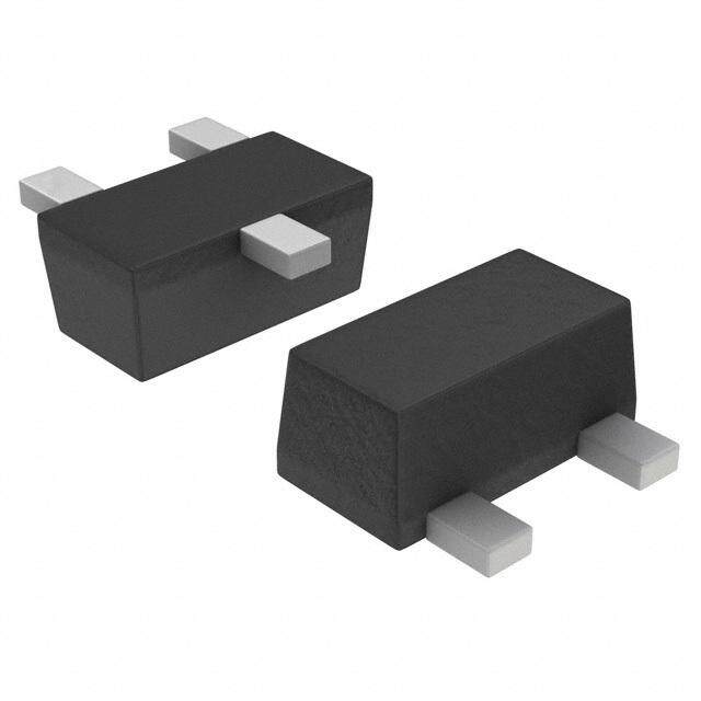
2STF2360 Low voltage fast-switching PNP power transistors Datasheet - production data Applications 4 • Emergency lighting 3 2 • LED 1 • Voltage regulation SOT-89 • Relay drive Description Figure 1. Internal schematic diagram The device is PNP transistor manufactured using new “PB-HDC” (power bipolar high density current) technology. The resulting transistor shows exceptional high gain performances coupled with very low saturation voltage. Features • Very low collector-emitter saturation voltage • High current gain characteristic • Fast-switching speed Table 1. Device summary Order code Marking Package Packaging 2STF2360 2360 SOT-89 Tape and reel December 2014 DocID13309 Rev 6 1/11 This is information on a product in full production. www.st.com
Contents 2STF2360 Contents 1 Absolute maximum ratings . . . . . . . . . . . . . . . . . . . . . . . . . . . . . . . . . . . 3 2 Electrical characteristics . . . . . . . . . . . . . . . . . . . . . . . . . . . . . . . . . . . . . 4 2.1 Typical characteristics (curves) . . . . . . . . . . . . . . . . . . . . . . . . . . . . . . . . . 5 2.2 Test circuits . . . . . . . . . . . . . . . . . . . . . . . . . . . . . . . . . . . . . . . . . . . . . . . . . 6 3 Package mechanical data . . . . . . . . . . . . . . . . . . . . . . . . . . . . . . . . . . . . . 7 3.1 SOT-89 . . . . . . . . . . . . . . . . . . . . . . . . . . . . . . . . . . . . . . . . . . . . . . . . . . . . 7 4 Revision history . . . . . . . . . . . . . . . . . . . . . . . . . . . . . . . . . . . . . . . . . . . 10 2/11 DocID13309 Rev 6
2STF2360 Absolute maximum ratings 1 Absolute maximum ratings Table 2. Absolute maximum ratings Symbol Parameter Value Unit V Collector-base voltage (I = 0) -60 V CBO E V Collector-emitter voltage (I = 0) -60 V CEO B V Emitter-base voltage (I = 0) -6 V EBO C I Collector current -3 A C I Collector peak current (t < 5 ms) -5 A CM P I Base current -0.2 A B I Base peak current (t < 5 ms) -0.4 A BM P P Total dissipation at T = 25 °C 1.4 W TOT amb Storage temperature -65 to 150 °C Tstg Max. operating junction temperature 150 °C TJ Table 3. Thermal data Symbol Parameter SOT-89 Unit R (1) Thermal resistance junction-ambient ___ _Max 89 °C/W thJA 1. Device mounted on a PCB area of 1 cm2 DocID13309 Rev 6 3/11 11
Electrical characteristics 2STF2360 2 Electrical characteristics T = 25°C; unless otherwise specified. CASE Table 4. Electrical characteristics Symbol Parameter Test conditions Min. Typ. Max. Unit Collector cut-off current I V = - 60 V -100 nA CBO (I = 0) CB E Emitter cut-off current I V = - 6 V -100 nA EBO (I = 0) EB C V Base-emitter on voltage V = - 2 V I = - 100 mA -630 -650 -730 mV BE(on) CE C V (1) Collector-emitter IC = - 2 A IB = - 100 mA -200 -320 mV CE(sat) saturation voltage I = - 3 A _ I = - 150 mA -300 -500 mV C B Base-emitter saturation V (1) I = - 2 A _ I = -100 mA -0.9 -1.2 V BE(sat) voltage C B I = - 100 mA_ V = - 2 V 200 (1) DC current gain C CE hFE I = - 1 A _ V = - 2 V 160 400 C CE Resistive load Delay time I = - 3 A V = - 10 V 10 15 ns td C CC Rise time I = - I = - 300 mA 75 100 ns tr B(on) B(off) Storage time V = 5 V 250 350 ns ts BE(off) Fall time 35 50 ns tf f Transition frequency I = - 0.1 A __ V = - 10 V 130 MHz T C CE 1. Pulse test: pulse duration ≤ 300 µs, duty cycle ≤ 2 % 4/11 DocID13309 Rev 6
2STF2360 Electrical characteristics 2.1 Typical characteristics (curves) Figure 2. DC current gain (V = - 2 V) Figure 3. DC current gain (V = - 5 V) CE CE Figure 4. Collector emitter saturation voltage Figure 5. Base emitter saturation voltage (cid:57)(cid:38)(cid:40)(cid:11)(cid:86)(cid:20)(cid:68)(cid:87)(cid:12) (cid:62)(cid:57)(cid:64) (cid:55)(cid:45)(cid:32)(cid:20)(cid:21)(cid:24)(cid:3)(cid:131)(cid:38) (cid:55)(cid:45)(cid:32)(cid:21)(cid:24)(cid:131)(cid:3)(cid:38) (cid:19)(cid:17)(cid:20) (cid:55)(cid:45)(cid:32)(cid:16)(cid:23)(cid:19)(cid:131)(cid:3)(cid:38) (cid:19)(cid:17)(cid:19)(cid:20) (cid:19)(cid:17)(cid:19)(cid:19)(cid:20) (cid:19)(cid:17)(cid:19)(cid:20) (cid:19)(cid:17)(cid:20) (cid:20) (cid:44)(cid:70)(cid:20)(cid:3)(cid:62)(cid:19)(cid:36)(cid:64) Figure 6. Resistive load switching on Figure 7. Resistive load switching off DocID13309 Rev 6 5/11 11
Electrical characteristics 2STF2360 Figure 8. Capacitances 2.2 Test circuits Figure 9. Resistive load switching 1. Fast electronic switch 2. Non-inductive resistor 6/11 DocID13309 Rev 6
2STF2360 Package mechanical data 3 Package mechanical data In order to meet environmental requirements, ST offers these devices in different grades of ECOPACK® packages, depending on their level of environmental compliance. ECOPACK® specifications, grade definitions and product status are available at: www.st.com. ECOPACK® is an ST trademark. 3.1 SOT-89 Figure 10. SOT-89 package outline (cid:26)(cid:19)(cid:28)(cid:27)(cid:20)(cid:25)(cid:25)(cid:66)(cid:53)(cid:40)(cid:57)(cid:66)(cid:40) DocID13309 Rev 6 7/11 11
Package mechanical data 2STF2360 Table 5. SOT-89 mechanical data mm Dim. Min. Typ. Max. A 1.40 1.60 B 0.44 0.56 B1 0.36 0.48 C 0.35 0.44 C1 0.35 0.44 D 4.40 4.60 D1 1.62 1.83 D3 0.90 E 2.29 2.60 e 1.42 1.57 e1 2.92 3.07 H 3.94 4.25 H1 2.70 3.10 K 1° 8° L 0.89 1.20 R 0.25 b 90° 8/11 DocID13309 Rev 6
2STF2360 Package mechanical data Figure 11. SOT-89 recommended footprint (cid:41)(cid:82)(cid:82)(cid:87)(cid:83)(cid:85)(cid:76)(cid:81)(cid:87) DocID13309 Rev 6 9/11 11
Revision history 2STF2360 4 Revision history Table 6. Document revision history Date Revision Changes 13-Sep-2006 1 Initial release 02-Mar-2007 2 New graphics have been added 23-Jan-2009 3 Updated mechanical data 09-Oct-2009 4 Added 2STD2360T4 in TO-252 (DPAK) package 14-Oct-2009 5 Modified Table1 on page1. Removed SOT-223 and TO-250 (DPAK) packages. Update description in cover page, Table1: Device summary, Section1: Absolute maximum ratings, Table4: Electrical 05-Dec-2014 6 characteristics, Section2.1: Typical characteristics (curves) and Section3: Package mechanical data. Minor text changes. 10/11 DocID13309 Rev 6
2STF2360 IMPORTANT NOTICE – PLEASE READ CAREFULLY STMicroelectronics NV and its subsidiaries (“ST”) reserve the right to make changes, corrections, enhancements, modifications, and improvements to ST products and/or to this document at any time without notice. Purchasers should obtain the latest relevant information on ST products before placing orders. ST products are sold pursuant to ST’s terms and conditions of sale in place at the time of order acknowledgement. Purchasers are solely responsible for the choice, selection, and use of ST products and ST assumes no liability for application assistance or the design of Purchasers’ products. No license, express or implied, to any intellectual property right is granted by ST herein. Resale of ST products with provisions different from the information set forth herein shall void any warranty granted by ST for such product. ST and the ST logo are trademarks of ST. All other product or service names are the property of their respective owners. Information in this document supersedes and replaces information previously supplied in any prior versions of this document. © 2014 STMicroelectronics – All rights reserved DocID13309 Rev 6 11/11 11