ICGOO在线商城 > 分立半导体产品 > 晶体管 - 双极 (BJT) - 单 > NSS12100XV6T1G
 Datasheet下载
- 型号: NSS12100XV6T1G
- 制造商: ON Semiconductor
- 库位|库存: xxxx|xxxx
- 要求:
| 数量阶梯 | 香港交货 | 国内含税 |
| +xxxx | $xxxx | ¥xxxx |
查看当月历史价格
查看今年历史价格
NSS12100XV6T1G产品简介:
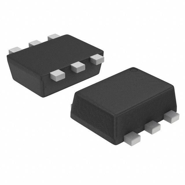
ICGOO电子元器件商城为您提供NSS12100XV6T1G由ON Semiconductor设计生产,在icgoo商城现货销售,并且可以通过原厂、代理商等渠道进行代购。 NSS12100XV6T1G价格参考。ON SemiconductorNSS12100XV6T1G封装/规格:晶体管 - 双极 (BJT) - 单, 双极 (BJT) 晶体管 PNP 12V 1A 500mW 表面贴装 SOT-563。您可以下载NSS12100XV6T1G参考资料、Datasheet数据手册功能说明书,资料中有NSS12100XV6T1G 详细功能的应用电路图电压和使用方法及教程。
ON Semiconductor(安森美半导体)的NSS12100XV6T1G是一款双极性晶体管(BJT),属于单晶体管类型。以下是该型号可能的应用场景:

1. 开关应用:
   NSS12100XV6T1G可以用作开关器件,在数字电路中实现信号的开启和关闭功能。例如,用于控制LED指示灯、继电器或其他低功率负载的通断。

2. 放大器电路:
   作为一款BJT晶体管,它可以用于音频信号放大、射频信号放大或电流放大等场景。例如,在小型音频设备中用作前置放大器或驱动级放大器。

3. 电源管理:
   在某些低功耗系统中,该晶体管可以用于简单的线性稳压器设计,或者作为电流限制元件来保护电路免受过流损害。

4. 电机驱动:
   对于小功率直流电机或步进电机,NSS12100XV6T1G可以用来驱动电机的正转、反转或制动操作。

5. 传感器接口:
   在工业自动化或消费电子领域,该晶体管可用于将传感器输出信号转换为适合后续处理的形式,比如将微弱信号放大到可检测水平。

6. 通信设备:
   在低频或中频通信电路中,这款晶体管能够执行调制、解调以及信号增强等功能。

7. 汽车电子:
   虽然具体参数需匹配要求,但该晶体管也可应用于车载环境下的简单控制任务,如车灯调节、风扇速度控制等。

总结来说,NSS12100XV6T1G适用于需要中小型电流处理能力的各种电子产品中,尤其在成本敏感且性能需求适中的场合表现良好。实际使用时应根据其电气特性(如最大集电极电流、电压耐受值等)进行合理选型与设计。
| 参数 | 数值 |
| 产品目录 | |
| 描述 | TRANSISTOR PNP 1A 12V SOT-563两极晶体管 - BJT 12V PNP LOW VCE(SAT) XTR |
| 产品分类 | 晶体管(BJT) - 单路分离式半导体 |
| 品牌 | ON Semiconductor |
| 产品手册 | |
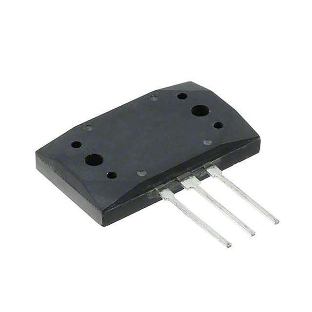
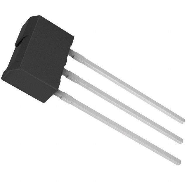
| 产品图片 |
|
| rohs | 符合RoHS无铅 / 符合限制有害物质指令(RoHS)规范要求 |
| 产品系列 | 晶体管,两极晶体管 - BJT,ON Semiconductor NSS12100XV6T1G- |
| 数据手册 | |
| 产品型号 | NSS12100XV6T1G |
| PCN设计/规格 | |
| 不同 Ib、Ic时的 Vce饱和值(最大值) | 440mV @ 100mA,1A |
| 不同 Ic、Vce 时的DC电流增益(hFE)(最小值) | 100 @ 500mA,2V |
| 产品培训模块 | http://www.digikey.cn/PTM/IndividualPTM.page?site=cn&lang=zhs&ptm=18613 |
| 产品目录页面 | |
| 产品种类 | 两极晶体管 - BJT |
| 供应商器件封装 | SOT-563 |
| 其它名称 | NSS12100XV6T1GOSCT |
| 功率-最大值 | 500mW |
| 包装 | 剪切带 (CT) |
| 发射极-基极电压VEBO | 5 V |
| 商标 | ON Semiconductor |
| 增益带宽产品fT | 100 MHz |
| 安装类型 | 表面贴装 |
| 安装风格 | SMD/SMT |
| 封装 | Reel |
| 封装/外壳 | SOT-563,SOT-666 |
| 封装/箱体 | SOT-563 |
| 工厂包装数量 | 4000 |
| 晶体管极性 | PNP |
| 晶体管类型 | PNP |
| 最大功率耗散 | 500 mW |
| 最大工作温度 | + 150 C |
| 最大直流电集电极电流 | 1 A |
| 最小工作温度 | - 55 C |
| 标准包装 | 1 |
| 电压-集射极击穿(最大值) | 12V |
| 电流-集电极(Ic)(最大值) | 1A |
| 电流-集电极截止(最大值) | - |
| 直流集电极/BaseGainhfeMin | 150 |
| 系列 | NSS12100XV6 |
| 配置 | Single |
| 集电极—发射极最大电压VCEO | - 12 V |
| 集电极—基极电压VCBO | - 12 V |
| 集电极—射极饱和电压 | - 400 mV |
| 集电极连续电流 | - 1 A |
| 频率-跃迁 | - |


- 商务部:美国ITC正式对集成电路等产品启动337调查
- 曝三星4nm工艺存在良率问题 高通将骁龙8 Gen1或转产台积电
- 太阳诱电将投资9.5亿元在常州建新厂生产MLCC 预计2023年完工
- 英特尔发布欧洲新工厂建设计划 深化IDM 2.0 战略
- 台积电先进制程称霸业界 有大客户加持明年业绩稳了
- 达到5530亿美元!SIA预计今年全球半导体销售额将创下新高
- 英特尔拟将自动驾驶子公司Mobileye上市 估值或超500亿美元
- 三星加码芯片和SET,合并消费电子和移动部门,撤换高东真等 CEO
- 三星电子宣布重大人事变动 还合并消费电子和移动部门
- 海关总署:前11个月进口集成电路产品价值2.52万亿元 增长14.8%


PDF Datasheet 数据手册内容提取
NSS12100XV6T1G 12 V, 1 A, Low V CE(sat) PNP Transistor ON Semiconductor’s e2PowerEdge family of low V CE(sat) transistors are miniature surface mount devices featuring ultra low saturation voltage (V ) and high current gain capability. These CE(sat) http://onsemi.com are designed for use in low voltage, high speed switching applications where affordable efficient energy control is important. Typical application are DC−DC converters and power management 12 VOLTS, 1.0 AMPS in portable and battery powered products such as cellular and cordless PNP LOW V TRANSISTOR CE(sat) phones, PDAs, computers, printers, digital cameras and MP3 players. EQUIVALENT R 300 m(cid:2) Other applications are low voltage motor controls in mass storage DS(on) products such as disc drives and tape drives. In the automotive industry they can be used in air bag deployment and in the instrument COLLECTOR cluster. The high current gain allows e2PowerEdge devices to be 1, 2, 5, 6 driven directly from PMU’s control outputs, and the Linear Gain (Beta) makes them ideal components in analog amplifiers. 3 BASE Features 4 • High Current Capability (1 A) EMITTER • High Power Handling (Up to 650 mW) • Low V (150 mV Typical @ 500 mA) CE(s) • Small Size • This is a Pb−Free Device 1 Benefits SOT−563 CASE 463A • High Specific Current and Power Capability Reduces Required PCB Area STYLE 4 • Reduced Parasitic Losses Increases Battery Life DEVICE MARKING MAXIMUM RATINGS (TA = 25°C) Rating Symbol Max Unit VE M(cid:2) (cid:2) Collector-Emitter Voltage VCEO −12 Vdc 1 Collector-Base Voltage VCBO −12 Vdc VE = Specific Device Code Emitter-Base Voltage VEBO −5.0 Vdc M = Month Code Collector Current − Continuous IC −1.0 Adc (cid:2) = Pb−Free Package Collector Current − Peak ICM −2.0 (Note: Microdot may be in either location) Electrostatic Discharge ESD HBM Class 3 MM Class C ORDERING INFORMATION Stresses exceeding Maximum Ratings may damage the device. Maximum Ratings are stress ratings only. Functional operation above the Recommended Operating Conditions is not implied. Extended exposure to stresses above the Device Package Shipping† Recommended Operating Conditions may affect device reliability. NSS12100XV6T1G SOT−563 4000/Tape & Reel (Pb−Free) †For information on tape and reel specifications, including part orientation and tape sizes, please refer to our Tape and Reel Packaging Specifications Brochure, BRD8011/D. © Semiconductor Components Industries, LLC, 2006 1 Publication Order Number: November, 2006 − Rev. 0 NSS12100XV6/D
NSS12100XV6T1G THERMAL CHARACTERISTICS Characteristic Symbol Max Unit Total Device Dissipation PD (Note 1) 500 mW TA = 25°C Derate above 25°C 4.0 mW/°C Thermal Resistance, R(cid:2)JA (Note 1) 250 °C/W Junction−to−Ambient Total Device Dissipation PD (Note 2) 650 mW TA = 25°C Derate above 25°C 5.2 mW/°C Thermal Resistance, R(cid:2)JA (Note 2) 192 °C/W Junction−to−Ambient Thermal Resistance, R(cid:2)JL 105 °C/W Junction−to−Lead 6 Total Device Dissipation PD Single 1.0 W (Single Pulse < 10 sec.) Junction and Storage TJ, Tstg −55 to +150 °C Temperature Range ELECTRICAL CHARACTERISTICS (TJ = 25°C unless otherwise noted) Characteristic Symbol Min Typ Max Unit OFF CHARACTERISTICS Collector−Emitter Breakdown Voltage, (IC = −10 mAdc, IB = 0) V(BR)CEO −12 − − Vdc Collector−Base Breakdown Voltage, (IC = −0.1 mAdc, IE = 0) V(BR)CBO −12 − − Vdc Emitter−Base Breakdown Voltage, (IE = −0.1 mAdc, IC = 0) V(BR)EBO −5.0 − − Vdc Collector Cutoff Current, (VCB = −12 Vdc, IE = 0) ICBO − −0.02 −0.1 (cid:3)Adc Emitter Cutoff Current, (VCES = −5.0 Vdc, IE = 0) IEBO − −0.03 −0.1 (cid:3)Adc ON CHARACTERISTICS DC Current Gain (Note 3) hFE (IC = −10 mA, VCE = −2.0 V) 200 − − (IC = −500 mA, VCE = −2.0 V) 100 − − (IC = −1.0 A, VCE = −2.0 V) 90 − − Collector−Emitter Saturation Voltage (Note 3) VCE(sat) V (IC = −0.05 A, IB = −0.005 A) (Note 4) − −0.030 −0.040 (IC = −0.1 A, IB = −0.002 A) − −0.080 −0.100 (IC = −0.1 A, IB = −0.010 A) − −0.050 −0.060 (IC = −0.5 A, IB = −0.050 A) − −0.200 −0.225 (IC = −1.0 A, IB = −0.100 A) − −0.400 −0.440 Base−Emitter Saturation Voltage (Note 3) VBE(sat) V (IC = −1.0 A, IB = −0.01 A) − 0.95 −1.15 Base−Emitter Turn−on Voltage (Note 3) VBE(on) V (IC = −2.0 A, VCE = −3.0 V) − −1.05 −1.15 Input Capacitance (VEB = −0.5 V, f = 1.0 MHz) Cibo − 50 pF Output Capacitance (VCB = −3.0 V, f = 1.0 MHz) Cobo − 20 pF 1. FR−4 @ 100 mm2, 1 oz copper traces. 2. FR−4 @ 500 mm2, 1 oz copper traces. 3. Pulsed Condition: Pulse Width = 300 (cid:3)sec, Duty Cycle ≤ 2%. 4. Guaranteed by design but not tested. http://onsemi.com 2
NSS12100XV6T1G 1.0 3.0 R 0.9 IC/IB = 10 VCE(sat) = 150°C R IC/IB = 100 VCE(sat) = −55°C 25°C MITTEE (V)0.8 25°C MITTEE (V)2.5 OR EOLTAG00..76 −55°C OR EOLTAG2.0 150°C ECTN V0.5 ECTN V1.5 LO LO OLTI0.4 OLTI , Cat)TURA0.3 , Cat)TURA1.0 E(sSA0.2 E(sSA0.5 C C V 0.1 V 0 0 0.001 0.01 0.1 1 10 0.001 0.01 0.1 1 10 IC, COLLECTOR CURRENT (A) IC, COLLECTOR CURRENT (A) Figure 1. Collector Emitter Saturation Voltage vs. Figure 2. Collector Emitter Saturation Voltage vs. Collector Current Collector Current 600 1.4 150°C (5.0 V) IC/IB = 10 1.2 AIN 500 150°C (2.0 V) ERE (V) G TG 1.0 NT 400 25°C (5.0 V) MITTA TA = −55°C E EOL 0.8 URR 300 25°C (2.0 V) ASE N V C BO 0.6 25°C , DC FE200 −−5555°°CC ((52..00 VV)) , BE(sat)TURATI 0.4 150°C h VA 100 S 0.2 0 0 0.001 0.01 0.1 1 10 0.001 0.01 0.1 1 10 IC, COLLECTOR CURRENT (A) IC, COLLECTOR CURRENT (A) Figure 3. DC Current Gain vs. Collector Figure 4. Base Emitter Saturation Voltage vs. Current Collector Current V) GE ( 1.4 V) 1.0 LTA VCE = −1.0 V GE ( 10 mA 100 mA 300 mA IC = 500 mA O 1.2 A N V OLT 0.8 O 1.0 V URN− 0.8 TA = −55°C TTER 0.6 R T EMI E 0.6 − T 25°C R 0.4 MIT TO E 0.4 C SE 150°C LLE 0.2 A 0.2 O B C , E(on) 00.001 0.01 0.1 1 10 V, CE 00.01 0.1 1 10 100 B V IC, COLLECTOR CURRENT (A) IB, BASE CURRENT (mA) Figure 5. Base Emitter Turn−On Voltage vs. Figure 6. Saturation Region Collector Current http://onsemi.com 3
NSS12100XV6T1G 50 30 F) F) p p E ( 45 E ( 25 NC NC Cobo(pF) TA 40 TA 20 CI Cibo(pF) CI A A AP 35 AP 15 C C T T PU 30 PU 10 N T C, Iibo 25 , OUbo 5 o C 20 0 0 1 2 3 4 5 0 1 2 3 4 5 6 7 8 9 10 VEB, EMITTER BASE VOLTAGE (V) VCB, COLLECTOR BASE VOLTAGE (V) Figure 7. Input Capacitance Figure 8. Output Capacitance http://onsemi.com 4
NSS12100XV6T1G PACKAGE DIMENSIONS SOT−563, 6 LEAD CASE 463A−01 ISSUE F D NOTES: A 1. DIMENSIONING AND TOLERANCING PER ANSI −X− Y14.5M, 1982. L 2. CONTROLLING DIMENSION: MILLIMETERS 3. MAXIMUM LEAD THICKNESS INCLUDES LEAD FINISH THICKNESS. MINIMUM LEAD THICKNESS 6 5 4 IS THE MINIMUM THICKNESS OF BASE MATERIAL. E −Y− HE MILLIMETERS INCHES 1 2 3 DIM MIN NOM MAX MIN NOM MAX A 0.50 0.55 0.60 0.020 0.021 0.023 b 0.17 0.22 0.27 0.007 0.009 0.011 b 65 PL C C 0.08 0.12 0.18 0.003 0.005 0.007 e 0.08 (0.003)M X Y DE 11..5100 11..6200 11..7300 00..005493 00..006427 00..006561 e 0.5 BSC 0.02 BSC L 0.10 0.20 0.30 0.004 0.008 0.012 HE 1.50 1.60 1.70 0.059 0.062 0.066 STYLE 4: PIN 1.COLLECTOR 2.COLLECTOR 3.BASE 4.EMITTER 5.COLLECTOR 6.COLLECTOR SOLDERING FOOTPRINT* 0.3 0.0118 0.45 0.0177 1.0 1.35 0.0394 0.0531 0.5 0.5 0.0197 0.0197 (cid:2) (cid:3) mm SCALE 20:1 inches *For additional information on our Pb−Free strategy and soldering details, please download the ON Semiconductor Soldering and Mounting Techniques Reference Manual, SOLDERRM/D. ON Semiconductor and are registered trademarks of Semiconductor Components Industries, LLC (SCILLC). SCILLC reserves the right to make changes without further notice to any products herein. SCILLC makes no warranty, representation or guarantee regarding the suitability of its products for any particular purpose, nor does SCILLC assume any liability arising out of the application or use of any product or circuit, and specifically disclaims any and all liability, including without limitation special, consequential or incidental damages. “Typical” parameters which may be provided in SCILLC data sheets and/or specifications can and do vary in different applications and actual performance may vary over time. All operating parameters, including “Typicals” must be validated for each customer application by customer’s technical experts. SCILLC does not convey any license under its patent rights nor the rights of others. SCILLC products are not designed, intended, or authorized for use as components in systems intended for surgical implant into the body, or other applications intended to support or sustain life, or for any other application in which the failure of the SCILLC product could create a situation where personal injury or death may occur. Should Buyer purchase or use SCILLC products for any such unintended or unauthorized application, Buyer shall indemnify and hold SCILLC and its officers, employees, subsidiaries, affiliates, and distributors harmless against all claims, costs, damages, and expenses, and reasonable attorney fees arising out of, directly or indirectly, any claim of personal injury or death associated with such unintended or unauthorized use, even if such claim alleges that SCILLC was negligent regarding the design or manufacture of the part. SCILLC is an Equal Opportunity/Affirmative Action Employer. This literature is subject to all applicable copyright laws and is not for resale in any manner. PUBLICATION ORDERING INFORMATION LITERATURE FULFILLMENT: N. American Technical Support: 800−282−9855 Toll Free ON Semiconductor Website: www.onsemi.com Literature Distribution Center for ON Semiconductor USA/Canada P.O. Box 5163, Denver, Colorado 80217 USA Europe, Middle East and Africa Technical Support: Order Literature: http://www.onsemi.com/orderlit Phone: 303−675−2175 or 800−344−3860 Toll Free USA/Canada Phone: 421 33 790 2910 Fax: 303−675−2176 or 800−344−3867 Toll Free USA/Canada Japan Customer Focus Center For additional information, please contact your local Email: orderlit@onsemi.com Phone: 81−3−5773−3850 Sales Representative http://onsemi.com NSS12100XV63/D 5