ICGOO在线商城 > 分立半导体产品 > 晶体管 - 双极 (BJT) - 单 > MJH11021G
 Datasheet下载
- 型号: MJH11021G
- 制造商: ON Semiconductor
- 库位|库存: xxxx|xxxx
- 要求:
| 数量阶梯 | 香港交货 | 国内含税 |
| +xxxx | $xxxx | ¥xxxx |
查看当月历史价格
查看今年历史价格
MJH11021G产品简介:
ICGOO电子元器件商城为您提供MJH11021G由ON Semiconductor设计生产,在icgoo商城现货销售,并且可以通过原厂、代理商等渠道进行代购。 MJH11021G价格参考。ON SemiconductorMJH11021G封装/规格:晶体管 - 双极 (BJT) - 单, Bipolar (BJT) Transistor PNP - Darlington 250V 15A 3MHz 150W Through Hole TO-247。您可以下载MJH11021G参考资料、Datasheet数据手册功能说明书,资料中有MJH11021G 详细功能的应用电路图电压和使用方法及教程。
ON Semiconductor(安森美)的型号MJH11021G是一款高压、高电流NPN型双极结型晶体管(BJT),属于单BJT产品类别。该器件专为高可靠性与高性能应用设计,广泛应用于工业、航空和汽车等对稳定性要求严苛的领域。

MJH11021G的主要应用场景包括:开关电源(SMPS)、DC-DC转换器、电机驱动电路、逆变器以及高功率放大电路。其高击穿电压(VCEO高达600V)和大电流承载能力(Ic可达15A)使其特别适合用于需要处理高电压和大电流的电力电子系统中。此外,该器件具备优良的热稳定性和可靠性,适用于高温或恶劣工作环境,如航空航天电源系统、工业控制设备和高可靠性电源模块。

由于采用TO-264封装,MJH11021G具有良好的散热性能,可有效降低热阻,提升长期运行的稳定性。其设计符合AEC-Q101车规级标准,也适用于部分高要求的汽车电子系统,如车载充电装置或电动车辆的辅助电源管理。

总之,MJH11021G凭借其高耐压、大电流、高可靠性和优异的热性能,主要应用于高端工业电源、航空航天电子、汽车电子及各类高功率开关与放大电路中,是关键功率控制环节的理想选择。
| 参数 | 数值 |
| 产品目录 | |
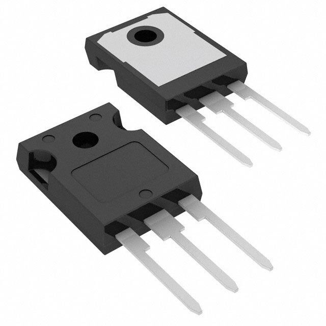
| 描述 | TRANS DARL PNP 15A 250V TO247达林顿晶体管 15A 250V Bipolar Power PNP |
| 产品分类 | 晶体管(BJT) - 单路分离式半导体 |
| 品牌 | ON Semiconductor |
| 产品手册 | |
| 产品图片 |
|
| rohs | 符合RoHS无铅 / 符合限制有害物质指令(RoHS)规范要求 |
| 产品系列 | 晶体管,达林顿晶体管,ON Semiconductor MJH11021G- |
| 数据手册 | |
| 产品型号 | MJH11021G |
| PCN封装 | |
| 不同 Ib、Ic时的 Vce饱和值(最大值) | 4V @ 150mA,15A |
| 不同 Ic、Vce 时的DC电流增益(hFE)(最小值) | 400 @ 10A,5V |
| 产品目录页面 | |
| 产品种类 | |
| 供应商器件封装 | TO-247 |
| 其它名称 | MJH11021GOS |
| 功率-最大值 | 150W |
| 功率耗散 | 150 W |
| 包装 | 管件 |
| 发射极-基极电压VEBO | 5 V |
| 商标 | ON Semiconductor |
| 安装类型 | 通孔 |
| 安装风格 | Through Hole |
| 封装 | Tube |
| 封装/外壳 | TO-247-3 |
| 封装/箱体 | TO-247 |
| 工厂包装数量 | 30 |
| 晶体管极性 | PNP |
| 晶体管类型 | PNP - 达林顿 |
| 最大工作温度 | + 150 C |
| 最大直流电集电极电流 | 15 A |
| 最小工作温度 | - 65 C |
| 标准包装 | 30 |
| 电压-集射极击穿(最大值) | 250V |
| 电流-集电极(Ic)(最大值) | 15A |
| 电流-集电极截止(最大值) | 1mA |
| 直流集电极/BaseGainhfeMin | 100, 400 |
| 系列 | MJH11021 |
| 配置 | Single |
| 集电极—发射极最大电压VCEO | 250 V |
| 集电极—基极电压VCBO | 250 V |
| 集电极连续电流 | 15 A |
| 频率-跃迁 | 3MHz |


- 商务部:美国ITC正式对集成电路等产品启动337调查
- 曝三星4nm工艺存在良率问题 高通将骁龙8 Gen1或转产台积电
- 太阳诱电将投资9.5亿元在常州建新厂生产MLCC 预计2023年完工
- 英特尔发布欧洲新工厂建设计划 深化IDM 2.0 战略
- 台积电先进制程称霸业界 有大客户加持明年业绩稳了
- 达到5530亿美元!SIA预计今年全球半导体销售额将创下新高
- 英特尔拟将自动驾驶子公司Mobileye上市 估值或超500亿美元
- 三星加码芯片和SET,合并消费电子和移动部门,撤换高东真等 CEO
- 三星电子宣布重大人事变动 还合并消费电子和移动部门
- 海关总署:前11个月进口集成电路产品价值2.52万亿元 增长14.8%


PDF Datasheet 数据手册内容提取
MJH11017, MJH11019, MJH11021(cid:2)(PNP) MJH11018, MJH11020, MJH11022(cid:2)(NPN) Complementary Darlington Silicon Power Transistors www.onsemi.com These devices are designed for use as general purpose amplifiers, 15 AMPERE DARLINGTON low frequency switching and motor control applications. COMPLEMENTARY SILICON Features POWER TRANSISTORS • High DC Current Gain @ 10 Adc — hFE = 400 Min (All Types) 150−250 VOLTS, 150 WATTS • Collector−Emitter Sustaining Voltage V = 150 Vdc (Min) — MJH11018, 17 CEO(sus) NPN PNP = 200 Vdc (Min) — MJH11020, 19 COLLECTOR 2 COLLECTOR 2 = 250 Vdc (Min) — MJH11022, 21 • Low Collector−Emitter Saturation Voltage V = 1.2 V (Typ) @ I = 5.0 A BASE BASE CE(sat) C 1 1 = 1.8 V (Typ) @ I = 10 A C • Monolithic Construction • These are Pb−Free Devices EMITTER 3 EMITTER 3 MJH11018 MJH11017 MJH11020 MJH11019 MAXIMUM RATINGS MJH11022 MJH11021 Rating Symbol Max Unit Collector−Emitter Voltage VCEO Vdc MJH11018, MJH11017 150 MJH11020, MJH11019 200 MJH11022, MJH11021 250 SOT−93 (TO−218) Collector−Base Voltage VCB Vdc CASE 340D MJH11018, MJH11017 150 STYLE 1 MJH11020, MJH11019 200 MJH11022, MJH11021 250 1 2 Emitter−Base Voltage VEB 5.0 Vdc 3 Collector Current − Continuous IC 15 Adc − Peak (Note 1) 30 TO−247 CASE 340L Base Current IB 0.5 Adc STYLE 3 Total Device Dissipation @ TC = 25(cid:2)C PD 150 W Derate above 25(cid:2)C 1.2 W/(cid:2)C Operating and Storage Junction Temperature TJ, Tstg –(cid:2)65 to (cid:2)C Range +(cid:2)150 NOTE: Effective June 2012 this device will THERMAL CHARACTERISTICS be available only in the TO−247 package. Reference FPCN# 16827. Characteristic Symbol Max Unit Thermal Resistance, Junction−to−Case R(cid:2)JC 0.83 (cid:2)C/W Stresses exceeding those listed in the Maximum Ratings table may damage the device. If any of these limits are exceeded, device functionality should not be ORDERING INFORMATION assumed, damage may occur and reliability may be affected. See detailed ordering and shipping information in the package 1. Pulse Test: Pulse Width = 5.0 ms, Duty Cycle (cid:2) 10%. dimensions section on page 2 of this data sheet. © Semiconductor Components Industries, LLC, 2016 1 Publication Order Number: August, 2016 − Rev. 10 MJH11017/D
MJH11017, MJH11019, MJH11021 (PNP) MJH11018, MJH11020, MJH11022 (NPN) MARKING DIAGRAMS TO−247 TO−218 MJH110xx AYWWG AYWWG MJH110xx 1 BASE 3 EMITTER 1 BASE 3 EMITTER 2 COLLECTOR 2 COLLECTOR A =Assembly Location Y =Year WW =Work Week G =Pb−Free Package MJH110xx =Device Code xx = 17, 19, 21, 18, 20, 22 ORDERING INFORMATION Device Order Number Package Type Shipping MJH11017G TO−218 30 Units / Rail (Pb−Free) MJH11018G TO−218 30 Units / Rail (Pb−Free) MJH11019G TO−218 30 Units / Rail (Pb−Free) MJH11020G TO−218 30 Units / Rail (Pb−Free) MJH11021G TO−218 30 Units / Rail (Pb−Free) MJH11022G TO−218 30 Units / Rail (Pb−Free) MJH11017G TO−247 30 Units / Rail (Pb−Free) MJH11018G TO−247 30 Units / Rail (Pb−Free) MJH11019G TO−247 30 Units / Rail (Pb−Free) MJH11020G TO−247 30 Units / Rail (Pb−Free) MJH11021G TO−247 30 Units / Rail (Pb−Free) MJH11022G TO−247 30 Units / Rail (Pb−Free) www.onsemi.com 2
MJH11017, MJH11019, MJH11021 (PNP) MJH11018, MJH11020, MJH11022 (NPN) 160 140 S) T AT 120 W N ( 100 O TI A P 80 SI S DI 60 R E W O 40 P P, D 20 0 0 20 40 60 80 100 120 140 160 TC, CASE TEMPERATURE (°C) Figure 1. Power Derating ÎÎÎÎELEÎÎCTÎÎRICÎÎAL ÎÎCHAÎÎRAÎÎCTEÎÎRISÎÎTICÎÎS (TÎÎC =ÎÎ 25(cid:2)ÎÎC unÎÎlessÎÎ otheÎÎrwisÎÎe noÎÎted)ÎÎÎÎÎÎÎÎÎÎÎÎÎÎÎÎÎÎÎÎÎÎÎÎÎÎÎÎÎÎÎÎ ÎÎÎÎÎÎÎÎÎÎÎÎÎÎÎÎÎÎÎÎÎÎÎÎÎÎÎÎÎÎÎÎÎÎÎÎÎÎÎÎÎÎÎÎÎÎÎÎÎÎÎÎÎÎÎÎÎÎÎÎÎÎÎÎÎÎÎÎÎÎ Characteristic Symbol Min Max Unit ÎÎÎÎÎÎÎÎÎÎÎÎÎÎÎÎÎÎÎÎÎÎÎÎÎÎÎÎÎÎÎÎÎÎÎÎÎÎÎÎÎÎÎÎÎÎÎÎÎÎÎÎÎÎÎÎÎÎÎÎÎÎÎÎÎÎÎÎÎÎ OFF CHARACTERISTICS ÎÎColÎlectoÎr−EmÎitteÎr SusÎtainÎing VÎoltaÎge (NÎoteÎ 2) ÎÎÎÎÎÎÎÎÎÎÎÎVÎCEO(Îsus)ÎÎÎÎÎÎÎÎÎÎVdcÎ ÎÎÎ(IC =Î 0.1 ÎAdc,Î IB =Î 0) ÎÎÎÎÎÎÎÎÎÎMJÎH11Î017,Î MJHÎ110Î18 ÎÎÎÎÎÎÎ150ÎÎÎ−ÎÎÎÎÎ MJH11019, MJH11020 200 − ÎÎÎÎÎÎÎÎÎÎÎÎÎÎÎÎÎÎÎÎÎÎÎÎÎÎÎÎÎÎÎÎÎÎMJÎÎH11ÎÎ021,ÎÎ MJHÎÎ110ÎÎ22 ÎÎÎÎÎÎÎÎÎÎÎÎÎÎ250ÎÎÎÎÎÎ−ÎÎÎÎÎÎÎÎÎÎ ÎÎColÎlectoÎr CuÎtoff CÎurreÎnt ÎÎÎÎÎÎÎÎÎÎÎÎÎÎÎÎÎÎICEÎO ÎÎÎÎÎÎÎÎÎmÎAdcÎ (VCE = 75 Vdc, IB = 0) MJH11017, MJH11018 − 1.0 ÎÎÎ(VCEÎ = 10Î0 VÎdc, IÎB = 0Î) ÎÎÎÎÎÎÎÎÎMJÎH11Î019,Î MJHÎ110Î20 ÎÎÎÎÎÎÎ−ÎÎÎ1.Î0 ÎÎÎÎ ÎÎÎÎÎÎ(VCEÎÎ = 12ÎÎ5 VÎÎdc, IÎÎB = 0ÎÎ) ÎÎÎÎÎÎÎÎÎÎÎÎÎÎÎÎÎÎMJÎÎH11ÎÎ021,ÎÎ MJHÎÎ110ÎÎ22 ÎÎÎÎÎÎÎÎÎÎÎÎÎÎ−ÎÎÎÎÎÎ1.ÎÎ0 ÎÎÎÎÎÎÎÎ ÎÎColÎlectoÎr CuÎtoff CÎurreÎnt ÎÎÎÎÎÎÎÎÎÎÎÎÎÎÎÎÎÎICEÎV ÎÎÎÎÎÎÎÎÎmÎAdcÎ (VCE = Rated VCB, VBE(off) = 1.5 Vdc) − 0.5 ÎÎÎÎÎÎ(VCEÎÎ = RÎÎatedÎÎ VCBÎÎ, VBÎÎE(off)ÎÎ = 1.ÎÎ5 VdÎÎc, TÎÎJ = 1ÎÎ50(cid:2)ÎÎC) ÎÎÎÎÎÎÎÎÎÎÎÎÎÎÎÎÎÎÎÎÎÎÎÎÎÎÎÎÎÎ−ÎÎÎÎÎÎ5.ÎÎ0 ÎÎÎÎÎÎÎÎ ÎÎÎÎÎÎÎÎÎÎÎÎÎÎÎÎÎÎÎÎÎÎÎÎÎÎÎÎÎÎÎÎÎÎÎÎÎÎÎÎÎÎÎÎÎÎÎÎÎÎÎÎÎÎÎÎÎÎÎÎÎÎÎÎÎÎÎÎÎÎ Emitter Cutoff Current (VBE = 5.0 Vdc IC = 0) IEBO − 2.0 mAdc ÎÎÎÎÎÎÎÎÎÎÎÎÎÎÎÎÎÎÎÎÎÎÎÎÎÎÎÎÎÎÎÎÎÎÎÎÎÎÎÎÎÎÎÎÎÎÎÎÎÎÎÎÎÎÎÎÎÎÎÎÎÎÎÎÎÎÎÎÎÎ ON CHARACTERISTICS (Note 2) ÎÎDC ÎCurrÎent GÎainÎÎÎÎÎÎÎÎÎÎÎÎÎÎÎÎÎÎÎÎhFEÎÎÎÎÎÎÎÎÎÎÎ− Î ÎÎÎ(IC =Î 10 AÎdc, ÎVCEÎ = 5.Î0 VdÎc) ÎÎÎÎÎÎÎÎÎÎÎÎÎÎÎÎÎÎÎÎ400ÎÎÎ15,0Î00ÎÎÎÎ (IC = 15 Adc, VCE = 5.0 Vdc) 100 − ÎÎÎÎÎÎÎÎÎÎÎÎÎÎÎÎÎÎÎÎÎÎÎÎÎÎÎÎÎÎÎÎÎÎÎÎÎÎÎÎÎÎÎÎÎÎÎÎÎÎÎÎÎÎÎÎÎÎÎÎÎÎÎÎÎÎÎÎÎÎÎÎÎÎ Collector−Emitter Saturation Voltage VCE(sat) Vdc ÎÎÎ(IC =Î 10 AÎdc, ÎIB = Î100Î mA)ÎÎÎÎÎÎÎÎÎÎÎÎÎÎÎÎÎÎÎÎÎ−ÎÎÎ2.Î5 ÎÎÎÎ (IC = 15 Adc, IB = 150 mA) − 4.0 ÎÎÎÎÎÎÎÎÎÎÎÎÎÎÎÎÎÎÎÎÎÎÎÎÎÎÎÎÎÎÎÎÎÎÎÎÎÎÎÎÎÎÎÎÎÎÎÎÎÎÎÎÎÎÎÎÎÎÎÎÎÎÎÎÎÎÎÎÎÎÎÎÎÎ Base−Emitter On Voltage (IC = 10 A, VCE = 5.0 Vdc) VBE(on) − 2.8 Vdc ÎÎÎÎÎÎÎÎÎÎÎÎÎÎÎÎÎÎÎÎÎÎÎÎÎÎÎÎÎÎÎÎÎÎÎÎÎÎÎÎÎÎÎÎÎÎÎÎÎÎÎÎÎÎÎÎÎÎÎÎÎÎÎÎÎÎÎÎÎÎÎÎÎÎ Base−Emitter Saturation Voltage (IC = 15 Adc, IB = 150 mA) VBE(sat) − 3.8 Vdc ÎÎÎÎÎÎÎÎÎÎÎÎÎÎÎÎÎÎÎÎÎÎÎÎÎÎÎÎÎÎÎÎÎÎÎÎÎÎÎÎÎÎÎÎÎÎÎÎÎÎÎÎÎÎÎÎÎÎÎÎÎÎÎÎÎÎÎÎÎÎ DYNAMIC CHARACTERISTICS ÎÎÎÎÎÎÎÎÎÎÎÎÎÎÎÎÎÎÎÎÎÎÎÎÎÎÎÎÎÎÎÎÎÎÎÎÎÎÎÎÎÎÎÎÎÎÎÎÎÎÎÎÎÎÎÎÎÎÎÎÎÎÎÎÎÎÎÎÎÎ Current−Gain Bandwidth Product (IC = 10 Adc, VCE = 3.0 Vdc, f = 1.0 MHz) fT 3.0 − − ÎÎÎÎÎÎÎÎÎÎÎÎÎÎÎÎÎÎÎÎÎÎÎÎÎÎÎÎÎÎÎÎÎÎÎÎÎÎÎÎÎÎÎÎÎÎÎÎÎÎÎÎÎÎÎÎÎÎÎÎÎÎÎÎÎÎÎÎÎÎÎÎÎÎ Output Capacitance MJH11018, MJH11020, MJH11022 Cob − 400 pF ÎÎÎÎÎÎ(VCBÎÎ = 10ÎÎ VdÎÎc, IEÎÎ = 0,ÎÎ f = 0ÎÎ.1 MÎÎHz)ÎÎÎÎÎÎÎÎMÎÎJH1ÎÎ1017ÎÎ, MJÎÎH11ÎÎ019,ÎÎ MJHÎÎ110ÎÎ21 ÎÎÎÎÎÎÎÎÎÎÎÎÎÎ−ÎÎÎÎÎÎ60ÎÎ0 ÎÎÎÎÎÎÎÎ ÎÎÎÎSmÎÎall−SÎÎignaÎÎl CuÎÎrrentÎÎ GaiÎÎn (ICÎÎ = 1ÎÎ0 AdÎÎc, VCÎÎE =ÎÎ 3.0 ÎÎVdc,ÎÎ f = 1ÎÎ.0 kÎÎHz)ÎÎÎÎÎÎÎÎÎÎÎÎÎÎÎhfeÎÎÎÎÎÎÎ75ÎÎÎÎÎ−ÎÎÎÎÎÎÎ− ÎÎ ÎÎÎÎSWIÎÎTCHÎÎINGÎÎ CHÎÎARAÎÎCTEÎÎRISÎÎTICSÎÎÎÎÎÎÎÎÎÎÎÎÎÎÎÎÎÎÎÎÎÎÎÎÎÎÎÎÎÎÎÎÎÎÎÎÎÎÎÎÎÎÎÎÎÎÎÎÎÎÎ ÎÎÎÎÎÎÎÎÎÎÎÎÎÎÎÎÎÎÎÎÎÎÎÎÎÎÎÎÎÎÎÎÎÎÎÎÎÎÎÎÎÎÎÎÎÎÎÎÎÎÎÎÎÎÎÎÎÎTÎÎÎypiÎÎcal ÎÎÎÎÎÎÎÎÎÎ ÎÎÎÎÎÎÎÎÎÎÎÎÎÎÎÎÎÎÎÎCÎÎÎharaÎÎcterÎÎisticÎÎÎÎÎÎÎÎÎÎÎÎÎÎÎÎÎÎÎÎÎÎSÎÎymbÎÎol ÎÎÎÎÎÎNPNÎÎÎÎÎÎPNÎÎP ÎÎÎÎÎÎUnitÎÎ ÎÎÎÎDelÎÎay TiÎÎmeÎÎÎÎÎÎÎÎÎÎÎÎÎÎÎÎÎÎÎÎÎÎÎÎÎÎÎÎÎÎÎtdÎÎÎÎÎÎÎÎ150ÎÎÎÎÎÎ7ÎÎ5 ÎÎÎÎÎÎnsÎÎ ÎÎÎÎRiseÎÎ TimÎÎe ÎÎÎÎÎÎÎÎÎÎÎÎÎÎÎÎÎ(VCÎC = 1Î00 VÎ, IC Î= 10Î A, IÎB = 1Î00 mÎA ÎÎÎÎÎÎtrÎÎÎÎÎÎÎÎ1.2ÎÎÎÎÎÎ0.ÎÎ5 ÎÎÎÎÎÎ(cid:3)sÎÎ ÎÎÎÎStoÎÎrageÎÎ TimÎÎe ÎÎÎÎÎÎÎÎÎÎÎÎÎÎÎVÎBE(oÎff) =Î 5.0 ÎV) (SÎee FÎigurÎe 2)ÎÎÎÎÎÎÎtsÎÎÎÎÎÎÎÎ4.4ÎÎÎÎÎÎ2.ÎÎ7 ÎÎÎÎÎÎ(cid:3)sÎÎ ÎÎFallÎ TimÎe ÎÎÎÎÎÎÎÎÎÎÎÎÎÎÎÎÎÎÎÎÎÎtfÎÎÎÎ2.5ÎÎÎ2.Î5 ÎÎÎ(cid:3)sÎ 2. Pulse Test: Pulse Width = 300 (cid:3)s, Duty Cycle (cid:2) 2.0%. www.onsemi.com 3
MJH11017, MJH11019, MJH11021 (PNP) MJH11018, MJH11020, MJH11022 (NPN) VCC -100 V RC SCOPE TUT RB & RC varied to obtain desired current levels V2 RB D1, must be fast recovery types, e.g.: APPROX 1N5825 used above IB ≈ 100 mA +12 V MSD6100 used below IB ≈ 100 mA 0 51 D1 V1 APPROX +(cid:2)4.0 V -(cid:2)8.0 V 25 (cid:3)s For td and tr, D1 is disconnected and V2 = 0 tr, tf ≤ 10 ns Duty Cycle = 1.0% For NPN test circuit, reverse diode and voltage polarities. Figure 2. Switching Times Test Circuit 1.0 0.7 L D = 0.5 MA 0.5 ERD) THZE 0.3 0.2 NT ALI 0.2 EM 0.1 ANSINOR 0.1 0.05 R(cid:2)JC(t) = r(t) R(cid:2)JC P(pk) r(t), EFFECTIVE TRRESISTANCE (0000....00007352 S0.I0N2GLE PULSE 0.01 RTDPRJU E(cid:2)C(JpLACUkSD) R=E- T V 0TTIEM.CR8S E3A= °A I ACNPPT/( PpWS tkL1H) Y MOR FA(cid:2)WOJXCNR(t )POWER DUTtY1 CtY2CLE, D = t1/t2 0.01 0.01 0.020.03 0.05 0.1 0.2 0.3 0.5 1.0 2.0 3.0 5.0 10 20 30 50 100 200 300 500 1000 t, TIME (ms) Figure 3. Thermal Response FORWARD BIAS S) TC = 25°C SINGLE PULSE There are two limitations on the power handling ability of P AM3200 0.1 ms a transistor: average junction temperature and second NT ( breakdown. Safe operating area curves indicate IC − VCE E10 0.5 ms R limits of the transistor that must be observed for reliable R CU5.0 1.0 ms operation; i.e., the transistor must not be subjected to greater OR 5.0 ms dissipation than the curves indicate. T2.0 dc EC WIRE BOND LIMIT The data of Figure 4 is based on TJ(pk) = 150(cid:2)C; TC is OLL1.0 THERMAL LIMIT variable depending on conditions. Second breakdown pulse I, CC00..52 SECOND BREAKDOWMMNJJ HHL11IM1100IT1179,, MMJJHH1111001280 l(cid:2)im 1it5s0 a(cid:2)rCe. vTalJi(dp kf)o rm dauyt yb ec yccalelcsu tloa te1d0 %fr opmro vtihdee dd aTtaJ( pikn) MJH11021, MJH11022 Figure 3. At high case temperatures, thermal limitations will 0 2.0 3.0 5.0 10 20 30 50 100150 250 reduce the power that can be handled to values less than the VCE, COLLECTOR-EMITTER VOLTAGE (VOLTS) limitations imposed by second breakdown. Figure 4. Maximum Rated Forward Bias Safe Operating Area (FBSOA) www.onsemi.com 4
MJH11017, MJH11019, MJH11021 (PNP) MJH11018, MJH11020, MJH11022 (NPN) REVERSE BIAS 30 For inductive loads, high voltage and high current must be PS) L = 200 (cid:3)H sustained simultaneously during turn−off, in most cases, NT (AM 20 ITCC/I B=1 1 ≥0 05°0C wcointhd itthieo nbsa sthe et oc oelmleicttteorr jvuonlcttaigoen mreuvsetr sbee bhiealsde dto. Ua nsdaefer tlheevseel RE VBE(off) = 0(cid:2)-(cid:2)5.0 V at or below a specific value of collector current. This can be CUR RBE = 47 (cid:4) accomplished by several means such as active clamping, RC R DUTY CYCLE = 10% O snubbing, load line shaping, etc. The safe level for these T EC 10 devices is specified as Reverse Bias Safe Operating Area L OL MJH11017, MJH11018 and represents the voltage−current conditions during C , C MJH11019, MJH11020 reverse biased turn−off. This rating is verified under I MJH11021, MJH11022 clamped conditions so that the device is never subjected to an avalanche mode. Figure 5 gives RBSOA characteristics. 0 0 20 60 100 140 180 220 260 VCE, COLLECTOR-EMITTER VOLTAGE (VOLTS) Figure 5. Maximum Rated Reverse Bias Safe Operating Area (RBSOA) PNP NPN 10,000 10,000 7000 VCE = 5.0 V VCE = 5.0 V 5000 5000 AIN 3000 AIN TC = 150°C T G 2000 TC = 150°C T G 2000 N N E E URR 1000 25°C URR 1000 25°C C C C C D 500 D 500 , FE , FE -(cid:2)55°C h h 200 -(cid:2)55°C 200 100 100 0.2 0.3 0.5 0.7 1.0 3.0 5.0 10 15 0.2 0.3 0.5 0.7 1.0 3.0 5.0 7.0 10 15 IC, COLLECTOR CURRENT (AMPS) IC, COLLECTOR CURRENT (AMPS) Figure 6. DC Current Gain www.onsemi.com 5
MJH11017, MJH11019, MJH11021 (PNP) MJH11018, MJH11020, MJH11022 (NPN) PNP NPN S) 4.5 S) 4.5 T T L L E (VO 4.0 TJ = 25°C E (VO 4.0 TJ = 25°C G G LTA 3.5 LTA 3.5 O O V V R 3.0 R E E 3.0 T T EMIT 2.5 EMIT 2.5 IC = 15 A - - OR IC = 15 A OR CT 2.0 CT 2.0 LE LE IC = 10 A OL 1.5 IC = 10 A OL 1.5 C C V, CE 1.0 IC = 5.0 A V, CE 1.0 IC = 5.0 A 1.0 2.03.0 5.0 10 20 30 50 100 200300 500 1000 1.0 2.03.0 5.0 10 20 30 50 100 200300 500 1000 IB, BASE CURRENT (mA) IB, BASE CURRENT (mA) Figure 7. Collector Saturation Region PNP NPN 4.0 4.0 3.5 TJ = 25°C 3.5 TJ = 25°C 3.0 3.0 S) S) T T OL 2.5 OL 2.5 V V E ( E ( G 2.0 VBE(sat) @ IC/IB = 100 G 2.0 VBE(sat) @ IC/IB = 100 A A T T L L O O V 1.5 V 1.5 1.0 VBE @ VCE = 5.0 V 1.0 VBE @ VCE = 5.0 V VCE(sat) @ IC/IB = 100 VCE(sat) @ IC/IB = 100 0.5 0.5 0.2 0.3 0.5 0.7 1.0 2.0 3.0 5.0 7.0 10 20 0.2 0.5 0.7 1.0 2.0 5.0 10 20 IC, COLLECTOR CURRENT (AMPS) IC, COLLECTOR CURRENT (AMPS) Figure 8. “On” Voltages PNP NPN MJH11017 COLLECTOR MJH11018 COLLECTOR MJH11019 MJH11020 MJH11021 MJH11022 BASE BASE EMITTER EMITTER Figure 9. Darlington Schematic www.onsemi.com 6
MJH11017, MJH11019, MJH11021 (PNP) MJH11018, MJH11020, MJH11022 (NPN) PACKAGE DIMENSIONS SOT−93 (TO−218) CASE 340D−02 ISSUE E C NOTES: 1.DIMENSIONING AND TOLERANCING PER ANSI B Q E Y14.5M, 1982. 2.CONTROLLING DIMENSION: MILLIMETER. MILLIMETERS INCHES DIM MIN MAX MIN MAX U 4 A --- 20.35 --- 0.801 A B 14.70 15.20 0.579 0.598 S L C 4.70 4.90 0.185 0.193 D 1.10 1.30 0.043 0.051 E 1.17 1.37 0.046 0.054 K 1 2 3 G 5.40 5.55 0.213 0.219 H 2.00 3.00 0.079 0.118 J 0.50 0.78 0.020 0.031 K 31.00 REF 1.220 REF L --- 16.20 --- 0.638 Q 4.00 4.10 0.158 0.161 S 17.80 18.20 0.701 0.717 U 4.00 REF 0.157 REF J V 1.75 REF 0.069 D H STYLE 1: PIN 1. BASE V 2. COLLECTOR G 3. EMITTER 4. COLLECTOR TO−247 CASE 340L−02 ISSUE F −T− NOTES: 1. DIMENSIONING AND TOLERANCING PER ANSI C Y14.5M, 1982. −B− 2. CONTROLLING DIMENSION: MILLIMETER. E MILLIMETERS INCHES U L DIM MIN MAX MIN MAX A 20.32 21.08 0.800 8.30 N 4 B 15.75 16.26 0.620 0.640 C 4.70 5.30 0.185 0.209 A −Q− D 1.00 1.40 0.040 0.055 E 1.90 2.60 0.075 0.102 1 2 3 0.63 (0.025) M T B M F 1.65 2.13 0.065 0.084 G 5.45 BSC 0.215 BSC H 1.50 2.49 0.059 0.098 P J 0.40 0.80 0.016 0.031 −Y− K 19.81 20.83 0.780 0.820 L 5.40 6.20 0.212 0.244 K N 4.32 5.49 0.170 0.216 P --- 4.50 --- 0.177 Q 3.55 3.65 0.140 0.144 U 6.15 BSC 0.242 BSC W 2.87 3.12 0.113 0.123 W J F2 PL H STYPLINE 13.:BASE G 2.COLLECTOR D3 PL 3.EMITTER 4.COLLECTOR 0.25 (0.010) M Y Q S www.onsemi.com 7
MJH11017, MJH11019, MJH11021 (PNP) MJH11018, MJH11020, MJH11022 (NPN) ON Semiconductor and are trademarks of Semiconductor Components Industries, LLC dba ON Semiconductor or its subsidiaries in the United States and/or other countries. ON Semiconductor owns the rights to a number of patents, trademarks, copyrights, trade secrets, and other intellectual property. A listing of ON Semiconductor’s product/patent coverage may be accessed at www.onsemi.com/site/pdf/Patent−Marking.pdf. ON Semiconductor reserves the right to make changes without further notice to any products herein. ON Semiconductor makes no warranty, representation or guarantee regarding the suitability of its products for any particular purpose, nor does ON Semiconductor assume any liability arising out of the application or use of any product or circuit, and specifically disclaims any and all liability, including without limitation special, consequential or incidental damages. Buyer is responsible for its products and applications using ON Semiconductor products, including compliance with all laws, regulations and safety requirements or standards, regardless of any support or applications information provided by ON Semiconductor. “Typical” parameters which may be provided in ON Semiconductor data sheets and/or specifications can and do vary in different applications and actual performance may vary over time. All operating parameters, including “Typicals” must be validated for each customer application by customer’s technical experts. ON Semiconductor does not convey any license under its patent rights nor the rights of others. ON Semiconductor products are not designed, intended, or authorized for use as a critical component in life support systems or any FDA Class 3 medical devices or medical devices with a same or similar classification in a foreign jurisdiction or any devices intended for implantation in the human body. Should Buyer purchase or use ON Semiconductor products for any such unintended or unauthorized application, Buyer shall indemnify and hold ON Semiconductor and its officers, employees, subsidiaries, affiliates, and distributors harmless against all claims, costs, damages, and expenses, and reasonable attorney fees arising out of, directly or indirectly, any claim of personal injury or death associated with such unintended or unauthorized use, even if such claim alleges that ON Semiconductor was negligent regarding the design or manufacture of the part. ON Semiconductor is an Equal Opportunity/Affirmative Action Employer. This literature is subject to all applicable copyright laws and is not for resale in any manner. PUBLICATION ORDERING INFORMATION LITERATURE FULFILLMENT: N. American Technical Support: 800−282−9855 Toll Free ON Semiconductor Website: www.onsemi.com Literature Distribution Center for ON Semiconductor USA/Canada P.O. Box 5163, Denver, Colorado 80217 USA Europe, Middle East and Africa Technical Support: Order Literature: http://www.onsemi.com/orderlit Phone: 303−675−2175 or 800−344−3860 Toll Free USA/Canada Phone: 421 33 790 2910 Fax: 303−675−2176 or 800−344−3867 Toll Free USA/Canada Japan Customer Focus Center For additional information, please contact your local Email: orderlit@onsemi.com Phone: 81−3−5817−1050 Sales Representative www.onsemi.com MJH11017/D 8
Mouser Electronics Authorized Distributor Click to View Pricing, Inventory, Delivery & Lifecycle Information: O N Semiconductor: MJH11017G MJH11019G MJH11020G MJH11021G MJH11022G